JP2019220681A - 基板処理方法および基板処理装置 - Google Patents
基板処理方法および基板処理装置 Download PDFInfo
- Publication number
- JP2019220681A JP2019220681A JP2019090801A JP2019090801A JP2019220681A JP 2019220681 A JP2019220681 A JP 2019220681A JP 2019090801 A JP2019090801 A JP 2019090801A JP 2019090801 A JP2019090801 A JP 2019090801A JP 2019220681 A JP2019220681 A JP 2019220681A
- Authority
- JP
- Japan
- Prior art keywords
- substrate
- processing
- chamber
- film
- processing apparatus
- Prior art date
- Legal status (The legal status is an assumption and is not a legal conclusion. Google has not performed a legal analysis and makes no representation as to the accuracy of the status listed.)
- Granted
Links
Images


Classifications
-
- C—CHEMISTRY; METALLURGY
- C23—COATING METALLIC MATERIAL; COATING MATERIAL WITH METALLIC MATERIAL; CHEMICAL SURFACE TREATMENT; DIFFUSION TREATMENT OF METALLIC MATERIAL; COATING BY VACUUM EVAPORATION, BY SPUTTERING, BY ION IMPLANTATION OR BY CHEMICAL VAPOUR DEPOSITION, IN GENERAL; INHIBITING CORROSION OF METALLIC MATERIAL OR INCRUSTATION IN GENERAL
- C23C—COATING METALLIC MATERIAL; COATING MATERIAL WITH METALLIC MATERIAL; SURFACE TREATMENT OF METALLIC MATERIAL BY DIFFUSION INTO THE SURFACE, BY CHEMICAL CONVERSION OR SUBSTITUTION; COATING BY VACUUM EVAPORATION, BY SPUTTERING, BY ION IMPLANTATION OR BY CHEMICAL VAPOUR DEPOSITION, IN GENERAL
- C23C16/00—Chemical coating by decomposition of gaseous compounds, without leaving reaction products of surface material in the coating, i.e. chemical vapour deposition [CVD] processes
- C23C16/44—Chemical coating by decomposition of gaseous compounds, without leaving reaction products of surface material in the coating, i.e. chemical vapour deposition [CVD] processes characterised by the method of coating
- C23C16/52—Controlling or regulating the coating process
-
- C—CHEMISTRY; METALLURGY
- C23—COATING METALLIC MATERIAL; COATING MATERIAL WITH METALLIC MATERIAL; CHEMICAL SURFACE TREATMENT; DIFFUSION TREATMENT OF METALLIC MATERIAL; COATING BY VACUUM EVAPORATION, BY SPUTTERING, BY ION IMPLANTATION OR BY CHEMICAL VAPOUR DEPOSITION, IN GENERAL; INHIBITING CORROSION OF METALLIC MATERIAL OR INCRUSTATION IN GENERAL
- C23C—COATING METALLIC MATERIAL; COATING MATERIAL WITH METALLIC MATERIAL; SURFACE TREATMENT OF METALLIC MATERIAL BY DIFFUSION INTO THE SURFACE, BY CHEMICAL CONVERSION OR SUBSTITUTION; COATING BY VACUUM EVAPORATION, BY SPUTTERING, BY ION IMPLANTATION OR BY CHEMICAL VAPOUR DEPOSITION, IN GENERAL
- C23C16/00—Chemical coating by decomposition of gaseous compounds, without leaving reaction products of surface material in the coating, i.e. chemical vapour deposition [CVD] processes
- C23C16/44—Chemical coating by decomposition of gaseous compounds, without leaving reaction products of surface material in the coating, i.e. chemical vapour deposition [CVD] processes characterised by the method of coating
- C23C16/455—Chemical coating by decomposition of gaseous compounds, without leaving reaction products of surface material in the coating, i.e. chemical vapour deposition [CVD] processes characterised by the method of coating characterised by the method used for introducing gases into reaction chamber or for modifying gas flows in reaction chamber
-
- C—CHEMISTRY; METALLURGY
- C23—COATING METALLIC MATERIAL; COATING MATERIAL WITH METALLIC MATERIAL; CHEMICAL SURFACE TREATMENT; DIFFUSION TREATMENT OF METALLIC MATERIAL; COATING BY VACUUM EVAPORATION, BY SPUTTERING, BY ION IMPLANTATION OR BY CHEMICAL VAPOUR DEPOSITION, IN GENERAL; INHIBITING CORROSION OF METALLIC MATERIAL OR INCRUSTATION IN GENERAL
- C23C—COATING METALLIC MATERIAL; COATING MATERIAL WITH METALLIC MATERIAL; SURFACE TREATMENT OF METALLIC MATERIAL BY DIFFUSION INTO THE SURFACE, BY CHEMICAL CONVERSION OR SUBSTITUTION; COATING BY VACUUM EVAPORATION, BY SPUTTERING, BY ION IMPLANTATION OR BY CHEMICAL VAPOUR DEPOSITION, IN GENERAL
- C23C16/00—Chemical coating by decomposition of gaseous compounds, without leaving reaction products of surface material in the coating, i.e. chemical vapour deposition [CVD] processes
- C23C16/02—Pretreatment of the material to be coated
- C23C16/0272—Deposition of sub-layers, e.g. to promote the adhesion of the main coating
-
- C—CHEMISTRY; METALLURGY
- C23—COATING METALLIC MATERIAL; COATING MATERIAL WITH METALLIC MATERIAL; CHEMICAL SURFACE TREATMENT; DIFFUSION TREATMENT OF METALLIC MATERIAL; COATING BY VACUUM EVAPORATION, BY SPUTTERING, BY ION IMPLANTATION OR BY CHEMICAL VAPOUR DEPOSITION, IN GENERAL; INHIBITING CORROSION OF METALLIC MATERIAL OR INCRUSTATION IN GENERAL
- C23C—COATING METALLIC MATERIAL; COATING MATERIAL WITH METALLIC MATERIAL; SURFACE TREATMENT OF METALLIC MATERIAL BY DIFFUSION INTO THE SURFACE, BY CHEMICAL CONVERSION OR SUBSTITUTION; COATING BY VACUUM EVAPORATION, BY SPUTTERING, BY ION IMPLANTATION OR BY CHEMICAL VAPOUR DEPOSITION, IN GENERAL
- C23C16/00—Chemical coating by decomposition of gaseous compounds, without leaving reaction products of surface material in the coating, i.e. chemical vapour deposition [CVD] processes
- C23C16/04—Coating on selected surface areas, e.g. using masks
- C23C16/045—Coating cavities or hollow spaces, e.g. interior of tubes; Infiltration of porous substrates
-
- C—CHEMISTRY; METALLURGY
- C23—COATING METALLIC MATERIAL; COATING MATERIAL WITH METALLIC MATERIAL; CHEMICAL SURFACE TREATMENT; DIFFUSION TREATMENT OF METALLIC MATERIAL; COATING BY VACUUM EVAPORATION, BY SPUTTERING, BY ION IMPLANTATION OR BY CHEMICAL VAPOUR DEPOSITION, IN GENERAL; INHIBITING CORROSION OF METALLIC MATERIAL OR INCRUSTATION IN GENERAL
- C23C—COATING METALLIC MATERIAL; COATING MATERIAL WITH METALLIC MATERIAL; SURFACE TREATMENT OF METALLIC MATERIAL BY DIFFUSION INTO THE SURFACE, BY CHEMICAL CONVERSION OR SUBSTITUTION; COATING BY VACUUM EVAPORATION, BY SPUTTERING, BY ION IMPLANTATION OR BY CHEMICAL VAPOUR DEPOSITION, IN GENERAL
- C23C16/00—Chemical coating by decomposition of gaseous compounds, without leaving reaction products of surface material in the coating, i.e. chemical vapour deposition [CVD] processes
- C23C16/22—Chemical coating by decomposition of gaseous compounds, without leaving reaction products of surface material in the coating, i.e. chemical vapour deposition [CVD] processes characterised by the deposition of inorganic material, other than metallic material
- C23C16/24—Deposition of silicon only
-
- C—CHEMISTRY; METALLURGY
- C23—COATING METALLIC MATERIAL; COATING MATERIAL WITH METALLIC MATERIAL; CHEMICAL SURFACE TREATMENT; DIFFUSION TREATMENT OF METALLIC MATERIAL; COATING BY VACUUM EVAPORATION, BY SPUTTERING, BY ION IMPLANTATION OR BY CHEMICAL VAPOUR DEPOSITION, IN GENERAL; INHIBITING CORROSION OF METALLIC MATERIAL OR INCRUSTATION IN GENERAL
- C23C—COATING METALLIC MATERIAL; COATING MATERIAL WITH METALLIC MATERIAL; SURFACE TREATMENT OF METALLIC MATERIAL BY DIFFUSION INTO THE SURFACE, BY CHEMICAL CONVERSION OR SUBSTITUTION; COATING BY VACUUM EVAPORATION, BY SPUTTERING, BY ION IMPLANTATION OR BY CHEMICAL VAPOUR DEPOSITION, IN GENERAL
- C23C16/00—Chemical coating by decomposition of gaseous compounds, without leaving reaction products of surface material in the coating, i.e. chemical vapour deposition [CVD] processes
- C23C16/22—Chemical coating by decomposition of gaseous compounds, without leaving reaction products of surface material in the coating, i.e. chemical vapour deposition [CVD] processes characterised by the deposition of inorganic material, other than metallic material
- C23C16/26—Deposition of carbon only
-
- C—CHEMISTRY; METALLURGY
- C23—COATING METALLIC MATERIAL; COATING MATERIAL WITH METALLIC MATERIAL; CHEMICAL SURFACE TREATMENT; DIFFUSION TREATMENT OF METALLIC MATERIAL; COATING BY VACUUM EVAPORATION, BY SPUTTERING, BY ION IMPLANTATION OR BY CHEMICAL VAPOUR DEPOSITION, IN GENERAL; INHIBITING CORROSION OF METALLIC MATERIAL OR INCRUSTATION IN GENERAL
- C23C—COATING METALLIC MATERIAL; COATING MATERIAL WITH METALLIC MATERIAL; SURFACE TREATMENT OF METALLIC MATERIAL BY DIFFUSION INTO THE SURFACE, BY CHEMICAL CONVERSION OR SUBSTITUTION; COATING BY VACUUM EVAPORATION, BY SPUTTERING, BY ION IMPLANTATION OR BY CHEMICAL VAPOUR DEPOSITION, IN GENERAL
- C23C16/00—Chemical coating by decomposition of gaseous compounds, without leaving reaction products of surface material in the coating, i.e. chemical vapour deposition [CVD] processes
- C23C16/44—Chemical coating by decomposition of gaseous compounds, without leaving reaction products of surface material in the coating, i.e. chemical vapour deposition [CVD] processes characterised by the method of coating
- C23C16/455—Chemical coating by decomposition of gaseous compounds, without leaving reaction products of surface material in the coating, i.e. chemical vapour deposition [CVD] processes characterised by the method of coating characterised by the method used for introducing gases into reaction chamber or for modifying gas flows in reaction chamber
- C23C16/45523—Pulsed gas flow or change of composition over time
- C23C16/45525—Atomic layer deposition [ALD]
- C23C16/45527—Atomic layer deposition [ALD] characterized by the ALD cycle, e.g. different flows or temperatures during half-reactions, unusual pulsing sequence, use of precursor mixtures or auxiliary reactants or activations
- C23C16/45534—Use of auxiliary reactants other than used for contributing to the composition of the main film, e.g. catalysts, activators or scavengers
-
- C—CHEMISTRY; METALLURGY
- C23—COATING METALLIC MATERIAL; COATING MATERIAL WITH METALLIC MATERIAL; CHEMICAL SURFACE TREATMENT; DIFFUSION TREATMENT OF METALLIC MATERIAL; COATING BY VACUUM EVAPORATION, BY SPUTTERING, BY ION IMPLANTATION OR BY CHEMICAL VAPOUR DEPOSITION, IN GENERAL; INHIBITING CORROSION OF METALLIC MATERIAL OR INCRUSTATION IN GENERAL
- C23C—COATING METALLIC MATERIAL; COATING MATERIAL WITH METALLIC MATERIAL; SURFACE TREATMENT OF METALLIC MATERIAL BY DIFFUSION INTO THE SURFACE, BY CHEMICAL CONVERSION OR SUBSTITUTION; COATING BY VACUUM EVAPORATION, BY SPUTTERING, BY ION IMPLANTATION OR BY CHEMICAL VAPOUR DEPOSITION, IN GENERAL
- C23C16/00—Chemical coating by decomposition of gaseous compounds, without leaving reaction products of surface material in the coating, i.e. chemical vapour deposition [CVD] processes
- C23C16/44—Chemical coating by decomposition of gaseous compounds, without leaving reaction products of surface material in the coating, i.e. chemical vapour deposition [CVD] processes characterised by the method of coating
- C23C16/455—Chemical coating by decomposition of gaseous compounds, without leaving reaction products of surface material in the coating, i.e. chemical vapour deposition [CVD] processes characterised by the method of coating characterised by the method used for introducing gases into reaction chamber or for modifying gas flows in reaction chamber
- C23C16/45523—Pulsed gas flow or change of composition over time
- C23C16/45525—Atomic layer deposition [ALD]
- C23C16/45527—Atomic layer deposition [ALD] characterized by the ALD cycle, e.g. different flows or temperatures during half-reactions, unusual pulsing sequence, use of precursor mixtures or auxiliary reactants or activations
- C23C16/45536—Use of plasma, radiation or electromagnetic fields
-
- C—CHEMISTRY; METALLURGY
- C23—COATING METALLIC MATERIAL; COATING MATERIAL WITH METALLIC MATERIAL; CHEMICAL SURFACE TREATMENT; DIFFUSION TREATMENT OF METALLIC MATERIAL; COATING BY VACUUM EVAPORATION, BY SPUTTERING, BY ION IMPLANTATION OR BY CHEMICAL VAPOUR DEPOSITION, IN GENERAL; INHIBITING CORROSION OF METALLIC MATERIAL OR INCRUSTATION IN GENERAL
- C23C—COATING METALLIC MATERIAL; COATING MATERIAL WITH METALLIC MATERIAL; SURFACE TREATMENT OF METALLIC MATERIAL BY DIFFUSION INTO THE SURFACE, BY CHEMICAL CONVERSION OR SUBSTITUTION; COATING BY VACUUM EVAPORATION, BY SPUTTERING, BY ION IMPLANTATION OR BY CHEMICAL VAPOUR DEPOSITION, IN GENERAL
- C23C16/00—Chemical coating by decomposition of gaseous compounds, without leaving reaction products of surface material in the coating, i.e. chemical vapour deposition [CVD] processes
- C23C16/44—Chemical coating by decomposition of gaseous compounds, without leaving reaction products of surface material in the coating, i.e. chemical vapour deposition [CVD] processes characterised by the method of coating
- C23C16/50—Chemical coating by decomposition of gaseous compounds, without leaving reaction products of surface material in the coating, i.e. chemical vapour deposition [CVD] processes characterised by the method of coating using electric discharges
- C23C16/505—Chemical coating by decomposition of gaseous compounds, without leaving reaction products of surface material in the coating, i.e. chemical vapour deposition [CVD] processes characterised by the method of coating using electric discharges using radio frequency discharges
- C23C16/507—Chemical coating by decomposition of gaseous compounds, without leaving reaction products of surface material in the coating, i.e. chemical vapour deposition [CVD] processes characterised by the method of coating using electric discharges using radio frequency discharges using external electrodes, e.g. in tunnel type reactors
-
- C—CHEMISTRY; METALLURGY
- C23—COATING METALLIC MATERIAL; COATING MATERIAL WITH METALLIC MATERIAL; CHEMICAL SURFACE TREATMENT; DIFFUSION TREATMENT OF METALLIC MATERIAL; COATING BY VACUUM EVAPORATION, BY SPUTTERING, BY ION IMPLANTATION OR BY CHEMICAL VAPOUR DEPOSITION, IN GENERAL; INHIBITING CORROSION OF METALLIC MATERIAL OR INCRUSTATION IN GENERAL
- C23C—COATING METALLIC MATERIAL; COATING MATERIAL WITH METALLIC MATERIAL; SURFACE TREATMENT OF METALLIC MATERIAL BY DIFFUSION INTO THE SURFACE, BY CHEMICAL CONVERSION OR SUBSTITUTION; COATING BY VACUUM EVAPORATION, BY SPUTTERING, BY ION IMPLANTATION OR BY CHEMICAL VAPOUR DEPOSITION, IN GENERAL
- C23C16/00—Chemical coating by decomposition of gaseous compounds, without leaving reaction products of surface material in the coating, i.e. chemical vapour deposition [CVD] processes
- C23C16/44—Chemical coating by decomposition of gaseous compounds, without leaving reaction products of surface material in the coating, i.e. chemical vapour deposition [CVD] processes characterised by the method of coating
- C23C16/50—Chemical coating by decomposition of gaseous compounds, without leaving reaction products of surface material in the coating, i.e. chemical vapour deposition [CVD] processes characterised by the method of coating using electric discharges
- C23C16/515—Chemical coating by decomposition of gaseous compounds, without leaving reaction products of surface material in the coating, i.e. chemical vapour deposition [CVD] processes characterised by the method of coating using electric discharges using pulsed discharges
-
- C—CHEMISTRY; METALLURGY
- C23—COATING METALLIC MATERIAL; COATING MATERIAL WITH METALLIC MATERIAL; CHEMICAL SURFACE TREATMENT; DIFFUSION TREATMENT OF METALLIC MATERIAL; COATING BY VACUUM EVAPORATION, BY SPUTTERING, BY ION IMPLANTATION OR BY CHEMICAL VAPOUR DEPOSITION, IN GENERAL; INHIBITING CORROSION OF METALLIC MATERIAL OR INCRUSTATION IN GENERAL
- C23C—COATING METALLIC MATERIAL; COATING MATERIAL WITH METALLIC MATERIAL; SURFACE TREATMENT OF METALLIC MATERIAL BY DIFFUSION INTO THE SURFACE, BY CHEMICAL CONVERSION OR SUBSTITUTION; COATING BY VACUUM EVAPORATION, BY SPUTTERING, BY ION IMPLANTATION OR BY CHEMICAL VAPOUR DEPOSITION, IN GENERAL
- C23C16/00—Chemical coating by decomposition of gaseous compounds, without leaving reaction products of surface material in the coating, i.e. chemical vapour deposition [CVD] processes
- C23C16/56—After-treatment
-
- H—ELECTRICITY
- H01—ELECTRIC ELEMENTS
- H01J—ELECTRIC DISCHARGE TUBES OR DISCHARGE LAMPS
- H01J37/00—Discharge tubes with provision for introducing objects or material to be exposed to the discharge, e.g. for the purpose of examination or processing thereof
- H01J37/32—Gas-filled discharge tubes
- H01J37/32009—Arrangements for generation of plasma specially adapted for examination or treatment of objects, e.g. plasma sources
- H01J37/32082—Radio frequency generated discharge
-
- H—ELECTRICITY
- H01—ELECTRIC ELEMENTS
- H01J—ELECTRIC DISCHARGE TUBES OR DISCHARGE LAMPS
- H01J37/00—Discharge tubes with provision for introducing objects or material to be exposed to the discharge, e.g. for the purpose of examination or processing thereof
- H01J37/32—Gas-filled discharge tubes
- H01J37/32431—Constructional details of the reactor
- H01J37/3244—Gas supply means
-
- H—ELECTRICITY
- H01—ELECTRIC ELEMENTS
- H01J—ELECTRIC DISCHARGE TUBES OR DISCHARGE LAMPS
- H01J37/00—Discharge tubes with provision for introducing objects or material to be exposed to the discharge, e.g. for the purpose of examination or processing thereof
- H01J37/32—Gas-filled discharge tubes
- H01J37/32431—Constructional details of the reactor
- H01J37/32715—Workpiece holder
-
- H—ELECTRICITY
- H01—ELECTRIC ELEMENTS
- H01J—ELECTRIC DISCHARGE TUBES OR DISCHARGE LAMPS
- H01J37/00—Discharge tubes with provision for introducing objects or material to be exposed to the discharge, e.g. for the purpose of examination or processing thereof
- H01J37/32—Gas-filled discharge tubes
- H01J37/32431—Constructional details of the reactor
- H01J37/32798—Further details of plasma apparatus not provided for in groups H01J37/3244 - H01J37/32788; special provisions for cleaning or maintenance of the apparatus
- H01J37/32899—Multiple chambers, e.g. cluster tools
-
- H—ELECTRICITY
- H05—ELECTRIC TECHNIQUES NOT OTHERWISE PROVIDED FOR
- H05H—PLASMA TECHNIQUE; PRODUCTION OF ACCELERATED ELECTRICALLY-CHARGED PARTICLES OR OF NEUTRONS; PRODUCTION OR ACCELERATION OF NEUTRAL MOLECULAR OR ATOMIC BEAMS
- H05H1/00—Generating plasma; Handling plasma
- H05H1/24—Generating plasma
- H05H1/46—Generating plasma using applied electromagnetic fields, e.g. high frequency or microwave energy
-
- H—ELECTRICITY
- H10—SEMICONDUCTOR DEVICES; ELECTRIC SOLID-STATE DEVICES NOT OTHERWISE PROVIDED FOR
- H10P—GENERIC PROCESSES OR APPARATUS FOR THE MANUFACTURE OR TREATMENT OF DEVICES COVERED BY CLASS H10
- H10P14/00—Formation of materials, e.g. in the shape of layers or pillars
- H10P14/60—Formation of materials, e.g. in the shape of layers or pillars of insulating materials
- H10P14/63—Formation of materials, e.g. in the shape of layers or pillars of insulating materials characterised by the formation processes
- H10P14/6302—Non-deposition formation processes
- H10P14/6318—Formation by simultaneous oxidation and nitridation
-
- H—ELECTRICITY
- H10—SEMICONDUCTOR DEVICES; ELECTRIC SOLID-STATE DEVICES NOT OTHERWISE PROVIDED FOR
- H10P—GENERIC PROCESSES OR APPARATUS FOR THE MANUFACTURE OR TREATMENT OF DEVICES COVERED BY CLASS H10
- H10P14/00—Formation of materials, e.g. in the shape of layers or pillars
- H10P14/60—Formation of materials, e.g. in the shape of layers or pillars of insulating materials
- H10P14/66—Formation of materials, e.g. in the shape of layers or pillars of insulating materials characterised by the type of materials
- H10P14/668—Formation of materials, e.g. in the shape of layers or pillars of insulating materials characterised by the type of materials the materials being characterised by the deposition precursor materials
-
- H—ELECTRICITY
- H10—SEMICONDUCTOR DEVICES; ELECTRIC SOLID-STATE DEVICES NOT OTHERWISE PROVIDED FOR
- H10P—GENERIC PROCESSES OR APPARATUS FOR THE MANUFACTURE OR TREATMENT OF DEVICES COVERED BY CLASS H10
- H10P14/00—Formation of materials, e.g. in the shape of layers or pillars
- H10P14/60—Formation of materials, e.g. in the shape of layers or pillars of insulating materials
- H10P14/69—Inorganic materials
- H10P14/6903—Inorganic materials containing silicon
-
- H—ELECTRICITY
- H10—SEMICONDUCTOR DEVICES; ELECTRIC SOLID-STATE DEVICES NOT OTHERWISE PROVIDED FOR
- H10P—GENERIC PROCESSES OR APPARATUS FOR THE MANUFACTURE OR TREATMENT OF DEVICES COVERED BY CLASS H10
- H10P50/00—Etching of wafers, substrates or parts of devices
-
- H—ELECTRICITY
- H10—SEMICONDUCTOR DEVICES; ELECTRIC SOLID-STATE DEVICES NOT OTHERWISE PROVIDED FOR
- H10P—GENERIC PROCESSES OR APPARATUS FOR THE MANUFACTURE OR TREATMENT OF DEVICES COVERED BY CLASS H10
- H10P50/00—Etching of wafers, substrates or parts of devices
- H10P50/20—Dry etching; Plasma etching; Reactive-ion etching
- H10P50/24—Dry etching; Plasma etching; Reactive-ion etching of semiconductor materials
- H10P50/242—Dry etching; Plasma etching; Reactive-ion etching of semiconductor materials of Group IV materials
-
- H—ELECTRICITY
- H10—SEMICONDUCTOR DEVICES; ELECTRIC SOLID-STATE DEVICES NOT OTHERWISE PROVIDED FOR
- H10P—GENERIC PROCESSES OR APPARATUS FOR THE MANUFACTURE OR TREATMENT OF DEVICES COVERED BY CLASS H10
- H10P72/00—Handling or holding of wafers, substrates or devices during manufacture or treatment thereof
- H10P72/04—Apparatus for manufacture or treatment
- H10P72/0402—Apparatus for fluid treatment
-
- H—ELECTRICITY
- H10—SEMICONDUCTOR DEVICES; ELECTRIC SOLID-STATE DEVICES NOT OTHERWISE PROVIDED FOR
- H10P—GENERIC PROCESSES OR APPARATUS FOR THE MANUFACTURE OR TREATMENT OF DEVICES COVERED BY CLASS H10
- H10P72/00—Handling or holding of wafers, substrates or devices during manufacture or treatment thereof
- H10P72/06—Apparatus for monitoring, sorting, marking, testing or measuring
- H10P72/0612—Production flow monitoring, e.g. for increasing throughput
-
- H—ELECTRICITY
- H01—ELECTRIC ELEMENTS
- H01J—ELECTRIC DISCHARGE TUBES OR DISCHARGE LAMPS
- H01J2237/00—Discharge tubes exposing object to beam, e.g. for analysis treatment, etching, imaging
- H01J2237/32—Processing objects by plasma generation
- H01J2237/33—Processing objects by plasma generation characterised by the type of processing
- H01J2237/332—Coating
- H01J2237/3321—CVD [Chemical Vapor Deposition]
-
- H—ELECTRICITY
- H01—ELECTRIC ELEMENTS
- H01J—ELECTRIC DISCHARGE TUBES OR DISCHARGE LAMPS
- H01J2237/00—Discharge tubes exposing object to beam, e.g. for analysis treatment, etching, imaging
- H01J2237/32—Processing objects by plasma generation
- H01J2237/33—Processing objects by plasma generation characterised by the type of processing
- H01J2237/334—Etching
-
- H—ELECTRICITY
- H10—SEMICONDUCTOR DEVICES; ELECTRIC SOLID-STATE DEVICES NOT OTHERWISE PROVIDED FOR
- H10P—GENERIC PROCESSES OR APPARATUS FOR THE MANUFACTURE OR TREATMENT OF DEVICES COVERED BY CLASS H10
- H10P14/00—Formation of materials, e.g. in the shape of layers or pillars
- H10P14/60—Formation of materials, e.g. in the shape of layers or pillars of insulating materials
- H10P14/63—Formation of materials, e.g. in the shape of layers or pillars of insulating materials characterised by the formation processes
- H10P14/6326—Deposition processes
- H10P14/6328—Deposition from the gas or vapour phase
- H10P14/6334—Deposition from the gas or vapour phase using decomposition or reaction of gaseous or vapour phase compounds, i.e. chemical vapour deposition
- H10P14/6336—Deposition from the gas or vapour phase using decomposition or reaction of gaseous or vapour phase compounds, i.e. chemical vapour deposition in the presence of a plasma [PECVD]
-
- H—ELECTRICITY
- H10—SEMICONDUCTOR DEVICES; ELECTRIC SOLID-STATE DEVICES NOT OTHERWISE PROVIDED FOR
- H10P—GENERIC PROCESSES OR APPARATUS FOR THE MANUFACTURE OR TREATMENT OF DEVICES COVERED BY CLASS H10
- H10P14/00—Formation of materials, e.g. in the shape of layers or pillars
- H10P14/60—Formation of materials, e.g. in the shape of layers or pillars of insulating materials
- H10P14/63—Formation of materials, e.g. in the shape of layers or pillars of insulating materials characterised by the formation processes
- H10P14/6326—Deposition processes
- H10P14/6328—Deposition from the gas or vapour phase
- H10P14/6334—Deposition from the gas or vapour phase using decomposition or reaction of gaseous or vapour phase compounds, i.e. chemical vapour deposition
- H10P14/6339—Deposition from the gas or vapour phase using decomposition or reaction of gaseous or vapour phase compounds, i.e. chemical vapour deposition deposition by cyclic CVD, e.g. ALD, ALE or pulsed CVD
-
- H—ELECTRICITY
- H10—SEMICONDUCTOR DEVICES; ELECTRIC SOLID-STATE DEVICES NOT OTHERWISE PROVIDED FOR
- H10P—GENERIC PROCESSES OR APPARATUS FOR THE MANUFACTURE OR TREATMENT OF DEVICES COVERED BY CLASS H10
- H10P14/00—Formation of materials, e.g. in the shape of layers or pillars
- H10P14/60—Formation of materials, e.g. in the shape of layers or pillars of insulating materials
- H10P14/68—Organic materials, e.g. photoresists
- H10P14/683—Organic materials, e.g. photoresists carbon-based polymeric organic materials, e.g. polyimides, poly cyclobutene or PVC
- H10P14/687—Organic materials, e.g. photoresists carbon-based polymeric organic materials, e.g. polyimides, poly cyclobutene or PVC the materials being fluorocarbon compounds, e.g. (CHxFy) n or polytetrafluoroethylene
-
- H—ELECTRICITY
- H10—SEMICONDUCTOR DEVICES; ELECTRIC SOLID-STATE DEVICES NOT OTHERWISE PROVIDED FOR
- H10P—GENERIC PROCESSES OR APPARATUS FOR THE MANUFACTURE OR TREATMENT OF DEVICES COVERED BY CLASS H10
- H10P50/00—Etching of wafers, substrates or parts of devices
- H10P50/20—Dry etching; Plasma etching; Reactive-ion etching
- H10P50/28—Dry etching; Plasma etching; Reactive-ion etching of insulating materials
- H10P50/282—Dry etching; Plasma etching; Reactive-ion etching of insulating materials of inorganic materials
- H10P50/283—Dry etching; Plasma etching; Reactive-ion etching of insulating materials of inorganic materials by chemical means
Landscapes
- Chemical & Material Sciences (AREA)
- Engineering & Computer Science (AREA)
- General Chemical & Material Sciences (AREA)
- Chemical Kinetics & Catalysis (AREA)
- Materials Engineering (AREA)
- Mechanical Engineering (AREA)
- Metallurgy (AREA)
- Organic Chemistry (AREA)
- Physics & Mathematics (AREA)
- Plasma & Fusion (AREA)
- Analytical Chemistry (AREA)
- Electromagnetism (AREA)
- Inorganic Chemistry (AREA)
- Spectroscopy & Molecular Physics (AREA)
- Chemical Vapour Deposition (AREA)
- Automation & Control Theory (AREA)
- Formation Of Insulating Films (AREA)
- Cleaning Or Drying Semiconductors (AREA)
- Plasma Technology (AREA)
- Drying Of Semiconductors (AREA)
- Manufacturing Of Printed Circuit Boards (AREA)
Abstract
Description
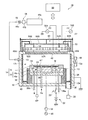
図1は、一実施形態に係る処理装置10の概略構成を示す図である。処理装置10は、一実施形態に係る基板処理装置の一例である。図1に示す処理装置10は、一実施形態に係る方法を実現するために使用できる。図1に示す処理装置10は、いわゆる誘導結合型プラズマ(Inductively-coupled plasma:ICP)装置であり、誘導結合型プラズマを生成するためのプラズマ源を有する。ただし、一実施形態に係る基板処理装置は、他の手法で生成されるプラズマを利用してもよい。たとえば、一実施形態に係る基板処理装置は、容量結合型プラズマ(CCP)、ECRプラズマ(electron-cyclotron-resonance plasma)、ヘリコン波励起プラズマ(HWP)、または、表面波プラズマ(SWP)等を利用する装置であってもよい。
図2は、一実施形態に係る処理方法の一例を示すフローチャートである。一実施形態に係る処理装置10は、半導体基板等のワークピースWを処理する。
ステップ102およびステップ103は、基板をチャンバ12から取り出すことなく実行する。つまり、第1処理および第2処理はチャンバ12内の真空状態を壊すことなく、in situで実行する。一実施形態に係る装置たとえば処理装置10は、気体供給部44を備え、気体供給部44はチャンバ12内に種々のガスを供給できる。また、一実施形態に係る装置は、第1処理および第2処理をチャンバ12内の真空状態を壊すことなく実行できる。また、一実施形態に係る装置は、排気路、排気口12e、排気装置3等の排気機構を備え、異なる種類のガスがチャンバ12内で混ざりあわないよう、パージ処理を実行できる。このため、一実施形態の装置は、ステップ102およびステップ103をin situで、または真空状態を壊すことなく実行できる。
また、一実施形態に係る装置は、プロセスごとにプラズマ生成の態様を変更してもよい。たとえば、コントローラ80は、アンテナ50と下部電極18とを制御して、第1処理の間は下部電極18のみに電圧が印加され、第2処理の間はアンテナ50のみに電圧が印加されるようにしてもよい。
一実施形態に係る装置においては、第1処理および第2処理に加えて、他の処理を第3処理としてin situで実行してもよい。たとえば、一実施形態に係る装置はさらにエッチング処理を実行することで、スループットをさらに向上させることができる。エッチング処理は原子層エッチング(ALE)処理であってもよい。
12 チャンバ
12c 空間
12e 排気口
12i 吸気口
12p 開口
13 支持機構
14 ステージ
16 静電チャック
18 下部電極
18a 第1プレート
18b 第2プレート
22 直流電源
23 スイッチ
24 流路
26a,26b パイプ
28 気体供給ライン
30 RF電源
32 整合器
34 シールド
36 パイプ
38 排気装置
40 バッフル板
42 ウィンドウ
44 気体供給部
44a ガス源
44b フローコントローラ
44c バルブ
46 パイプ
48 ゲートバルブ
50 アンテナ
52A 内側アンテナ素子
52B 外側アンテナ素子
54 クランプ
60 シールド
62A 内側シールド壁
62B 外側シールド壁
64A 内側シールド板
64B 外側シールド板
68A,68B アクチュエータ
70A,70B RF電源
80 コントローラ
FR フォーカスリング
HT ヒータ
HP ヒータ電源
W ワークピース
Claims (16)
- チャンバを備える処理装置と、
メモリと、当該メモリに接続されたプロセッサとを備えるコントローラと、
を備える基板処理装置であって、
前記メモリは前記プロセッサを制御して前記処理装置による処理を制御するための、コンピュータによって実行可能な命令を記憶し、当該処理は、
化学蒸着(CVD)により、前記チャンバ内の基板の第1領域内に第1膜を形成する第1処理と、
原子層堆積(ALD)により、前記チャンバ内の前記基板の第2領域内に第2膜を形成する第2処理と、
を含み、
前記第1処理および前記第2処理を、前記基板を前記チャンバから外に移動させることなく実行する、基板処理装置。 - 前記コントローラにより制御されるアンテナと、
前記アンテナに対向して配置され、前記基板を上に保持するよう構成され、前記コントローラにより制御される下部電極と、
をさらに備え、前記処理はさらに、
前記化学蒸着中に前記下部電極に電圧印加し、
前記原子層堆積の改質ステップ中に前記アンテナに電圧印加することを含む、請求項1に記載の基板処理装置。 - 前記チャンバ上に配置され、前記コントローラにより制御されるアンテナと、
前記アンテナに対向して配置され、前記基板を上に保持するよう構成され、前記コントローラにより制御される下部電極と、
をさらに備え、前記処理はさらに、
前記化学蒸着中に前記アンテナに電圧印加せずに、前記下部電極に電圧印加し、
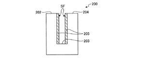
前記原子層堆積の改質ステップ中に前記下部電極に電圧印加せず、前記アンテナに電圧印加することを含む、請求項1に記載の基板処理装置。 - 前記第1処理は、前記基板の親水性表面の第1領域上に疎水性表面として前記第1膜を形成し、
前記第2処理は、前記基板の前記疎水性表面の前記第2領域上に、ヒドロキシ基と反応する前駆体を吸着させることにより前記第2膜を形成する、請求項1〜3のいずれか1項に記載の基板処理装置。 - 前記第2処理は、前記基板から前記第1膜の少なくとも一部を除去する、請求項1〜4のいずれか1項に記載の基板処理装置。
- 前記第1処理は、フルオロカーボンプラズマにより前記第1膜を堆積する、請求項1〜5のいずれか1項に記載の基板処理装置。
- 前記第1処理は、前記下部電極に印加される電圧を制御することにより、異方性CVDおよび等方性CVDのいずれか一方を実行する、請求項2に記載の基板処理装置。
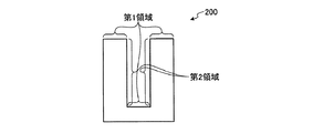
- 前記第1処理は、前記基板の凹凸の頂部および底部に前記第1膜を形成し、
前記第2処理は、前記基板の凹凸の側壁に前記第2膜を形成する、請求項1〜7のいずれか1項に記載の基板処理装置。 - 前記基板は、SiO2、SiN、SiおよびGeのうち少なくともいずれか一つを含有し、
前記第2処理は、前記第2膜としてシリコン含有膜を形成する、請求項1〜8のいずれか1項に記載の基板処理装置。 - 前記第1処理および前記第2処理は順に繰り返し実行される、請求項1〜9のいずれか1項に記載の基板処理装置。
- 前記第1処理および前記第2処理は、誘導結合型プラズマまたは容量結合型プラズマを使用して実行される、請求項1〜10のいずれか1項に記載の基板処理装置。
- チャンバを有する処理装置と、
メモリと、当該メモリに接続されるプロセッサと、を有するコントローラと、を備え、前記メモリは前記プロセッサを制御して処理を制御させるためのコンピュータにより実行可能な命令を記憶し、当該処理は、
化学蒸着により、前記チャンバ内の基板の第1領域内に第1膜を形成する第1処理と、
原子層堆積により、前記チャンバ内の前記基板の第2領域内に第2膜を形成する第2処理と、
前記基板をエッチングする第3処理と、
を含み、
前記第1処理、前記第2処理および前記第3処理を、前記チャンバの外に前記基板を移動させずに実行する、基板処理装置。 - 前記第3処理は、原子層エッチングを含み、
前記第3処理はさらに、
NプラズマおよびHプラズマの一方により前記基板の表面を改質し、
前記チャンバをパージし、
前記NプラズマおよびHプラズマの一方により改質された前記表面を、ハロゲンガスにより除去する、ことを含む、請求項12に記載の基板処理装置。 - 化学蒸着により、処理装置のチャンバ内の基板の第1領域内に第1膜を形成する第1処理と、
原子層堆積により、前記チャンバ内の前記基板の第2領域内に第2膜を形成する第2処理と、
を含み、
前記第1処理および前記第2処理は、前記チャンバの外に前記基板を移動させずに実行する、基板処理方法。 - 前記基板をエッチングする第3処理をさらに含み、
前記第1処理、前記第2処理および前記第3処理は、前記チャンバの外に前記基板を移動させずに実行する、請求項14に記載の基板処理方法。 - 前記第3処理は、原子層エッチングを含み、
前記第3処理はさらに、
NプラズマおよびHプラズマの一方により、前記基板の表面を改質し、
前記チャンバをパージし、
前記NプラズマおよびHプラズマの一方により改質された前記表面を、ハロゲンガスにより除去することを含む、請求項15に記載の基板処理方法。
Applications Claiming Priority (2)
| Application Number | Priority Date | Filing Date | Title |
|---|---|---|---|
| US16/010,800 | 2018-06-18 | ||
| US16/010,800 US10781519B2 (en) | 2018-06-18 | 2018-06-18 | Method and apparatus for processing substrate |
Publications (3)
| Publication Number | Publication Date |
|---|---|
| JP2019220681A true JP2019220681A (ja) | 2019-12-26 |
| JP2019220681A5 JP2019220681A5 (ja) | 2022-05-25 |
| JP7323330B2 JP7323330B2 (ja) | 2023-08-08 |
Family
ID=68839187
Family Applications (1)
| Application Number | Title | Priority Date | Filing Date |
|---|---|---|---|
| JP2019090801A Active JP7323330B2 (ja) | 2018-06-18 | 2019-05-13 | 基板処理方法および基板処理装置 |
Country Status (5)
| Country | Link |
|---|---|
| US (2) | US10781519B2 (ja) |
| JP (1) | JP7323330B2 (ja) |
| KR (1) | KR102734223B1 (ja) |
| CN (1) | CN110616416A (ja) |
| TW (1) | TWI807049B (ja) |
Families Citing this family (7)
| Publication number | Priority date | Publication date | Assignee | Title |
|---|---|---|---|---|
| TWI790372B (zh) | 2018-04-09 | 2023-01-21 | 日商東京威力科創股份有限公司 | 具有用於低電容內連線之氣隙的半導體元件形成方法 |
| US10896823B2 (en) * | 2018-11-21 | 2021-01-19 | Thomas E. Seidel | Limited dose atomic layer processes for localizing coatings on non-planar surfaces |
| JP7285152B2 (ja) * | 2019-07-08 | 2023-06-01 | 東京エレクトロン株式会社 | プラズマ処理装置 |
| US20220375763A1 (en) * | 2020-01-30 | 2022-11-24 | Sony Semiconductor Solutions Corporation | Semiconductor device and etching method |
| US20240404837A1 (en) * | 2023-05-30 | 2024-12-05 | Applied Materials, Inc. | Halogen-free etching of silicon nitride |
| CN118166339B (zh) * | 2024-01-31 | 2026-04-17 | 温州核芯智存科技有限公司 | 一种原子沉积腔室、设备、设备制造方法及电容制备方法 |
| US20250364210A1 (en) * | 2024-05-24 | 2025-11-27 | Applied Materials, Inc. | Pecvd trench bottom profile control with pulsed dual rf plasma |
Citations (2)
| Publication number | Priority date | Publication date | Assignee | Title |
|---|---|---|---|---|
| US9716005B1 (en) * | 2016-03-18 | 2017-07-25 | Applied Materials, Inc. | Plasma poisoning to enable selective deposition |
| US20180166270A1 (en) * | 2016-12-09 | 2018-06-14 | Wonik Ips Co., Ltd. | Method of depositing a thin film |
Family Cites Families (26)
| Publication number | Priority date | Publication date | Assignee | Title |
|---|---|---|---|---|
| US20020004309A1 (en) * | 1990-07-31 | 2002-01-10 | Kenneth S. Collins | Processes used in an inductively coupled plasma reactor |
| DE19651029C2 (de) * | 1996-12-09 | 1999-12-02 | Ibm | Kalibrierstandard für Profilometer und Herstellverfahren |
| US6794290B1 (en) * | 2001-12-03 | 2004-09-21 | Novellus Systems, Inc. | Method of chemical modification of structure topography |
| US6852996B2 (en) * | 2002-09-25 | 2005-02-08 | Stmicroelectronics, Inc. | Organic semiconductor sensor device |
| US7323231B2 (en) * | 2003-10-09 | 2008-01-29 | Micron Technology, Inc. | Apparatus and methods for plasma vapor deposition processes |
| US7476621B1 (en) * | 2003-12-10 | 2009-01-13 | Novellus Systems, Inc. | Halogen-free noble gas assisted H2 plasma etch process in deposition-etch-deposition gap fill |
| US8974868B2 (en) * | 2005-03-21 | 2015-03-10 | Tokyo Electron Limited | Post deposition plasma cleaning system and method |
| US7341959B2 (en) * | 2005-03-21 | 2008-03-11 | Tokyo Electron Limited | Plasma enhanced atomic layer deposition system and method |
| US8815014B2 (en) * | 2005-11-18 | 2014-08-26 | Tokyo Electron Limited | Method and system for performing different deposition processes within a single chamber |
| US7649239B2 (en) * | 2006-05-04 | 2010-01-19 | Intel Corporation | Dielectric spacers for metal interconnects and method to form the same |
| US20070298583A1 (en) * | 2006-06-27 | 2007-12-27 | Macronix International Co., Ltd. | Method for forming a shallow trench isolation region |
| JP4916257B2 (ja) * | 2006-09-06 | 2012-04-11 | 東京エレクトロン株式会社 | 酸化膜の形成方法、酸化膜の形成装置及びプログラム |
| WO2008153674A1 (en) * | 2007-06-09 | 2008-12-18 | Boris Kobrin | Method and apparatus for anisotropic etching |
| US8129288B2 (en) * | 2008-05-02 | 2012-03-06 | Intermolecular, Inc. | Combinatorial plasma enhanced deposition techniques |
| US7816278B2 (en) * | 2008-03-28 | 2010-10-19 | Tokyo Electron Limited | In-situ hybrid deposition of high dielectric constant films using atomic layer deposition and chemical vapor deposition |
| JP5439771B2 (ja) * | 2008-09-05 | 2014-03-12 | 東京エレクトロン株式会社 | 成膜装置 |
| US8039966B2 (en) * | 2009-09-03 | 2011-10-18 | International Business Machines Corporation | Structures of and methods and tools for forming in-situ metallic/dielectric caps for interconnects |
| US9257274B2 (en) * | 2010-04-15 | 2016-02-09 | Lam Research Corporation | Gapfill of variable aspect ratio features with a composite PEALD and PECVD method |
| US9564312B2 (en) * | 2014-11-24 | 2017-02-07 | Lam Research Corporation | Selective inhibition in atomic layer deposition of silicon-containing films |
| FR3032436B1 (fr) | 2015-02-10 | 2019-08-30 | Louis Vuitton Malletier | Dispositif de conditionnement pour un produit a distribuer |
| CN106148918B (zh) * | 2015-03-26 | 2018-08-07 | 理想晶延半导体设备(上海)有限公司 | 半导体处理设备 |
| US10037884B2 (en) * | 2016-08-31 | 2018-07-31 | Lam Research Corporation | Selective atomic layer deposition for gapfill using sacrificial underlayer |
| JP6559107B2 (ja) * | 2016-09-09 | 2019-08-14 | 東京エレクトロン株式会社 | 成膜方法および成膜システム |
| TWI805162B (zh) * | 2017-04-18 | 2023-06-11 | 日商東京威力科創股份有限公司 | 被處理體之處理裝置 |
| US10892186B2 (en) * | 2017-10-14 | 2021-01-12 | Applied Materials, Inc. | Integration of ALD copper with high temperature PVD copper deposition for BEOL interconnect |
| US10515815B2 (en) * | 2017-11-21 | 2019-12-24 | Lam Research Corporation | Atomic layer deposition and etch in a single plasma chamber for fin field effect transistor formation |
-
2018
- 2018-06-18 US US16/010,800 patent/US10781519B2/en active Active
-
2019
- 2019-05-13 JP JP2019090801A patent/JP7323330B2/ja active Active
- 2019-06-17 KR KR1020190071720A patent/KR102734223B1/ko active Active
- 2019-06-18 TW TW108121136A patent/TWI807049B/zh not_active IP Right Cessation
- 2019-06-18 CN CN201910525969.3A patent/CN110616416A/zh active Pending
-
2020
- 2020-08-21 US US17/000,090 patent/US12325919B2/en active Active
Patent Citations (2)
| Publication number | Priority date | Publication date | Assignee | Title |
|---|---|---|---|---|
| US9716005B1 (en) * | 2016-03-18 | 2017-07-25 | Applied Materials, Inc. | Plasma poisoning to enable selective deposition |
| US20180166270A1 (en) * | 2016-12-09 | 2018-06-14 | Wonik Ips Co., Ltd. | Method of depositing a thin film |
Also Published As
| Publication number | Publication date |
|---|---|
| JP7323330B2 (ja) | 2023-08-08 |
| US20210025060A1 (en) | 2021-01-28 |
| US20190382897A1 (en) | 2019-12-19 |
| US12325919B2 (en) | 2025-06-10 |
| US10781519B2 (en) | 2020-09-22 |
| CN110616416A (zh) | 2019-12-27 |
| KR102734223B1 (ko) | 2024-11-25 |
| KR20190142741A (ko) | 2019-12-27 |
| TWI807049B (zh) | 2023-07-01 |
| TW202002014A (zh) | 2020-01-01 |
Similar Documents
| Publication | Publication Date | Title |
|---|---|---|
| US10566209B2 (en) | Etching method and workpiece processing method | |
| JP7323330B2 (ja) | 基板処理方法および基板処理装置 | |
| KR102617192B1 (ko) | 질화 실리콘으로 형성된 제 1 영역을 산화 실리콘으로 형성된 제 2 영역에 대하여 선택적으로 에칭하는 방법 | |
| CN108878285B (zh) | 蚀刻方法 | |
| US12125710B2 (en) | Substrate processing method and substrate processing apparatus | |
| US20250022706A1 (en) | Substrate processing method and substrate processing apparatus | |
| KR20230129345A (ko) | 플라즈마 처리 장치 및 에칭 방법 | |
| JP2019186501A (ja) | エッチングする方法及びプラズマ処理装置 | |
| CN111527591A (zh) | 等离子体蚀刻方法和等离子体蚀刻装置 | |
| US10755944B2 (en) | Etching method and plasma processing apparatus | |
| US12476115B2 (en) | Method for processing workpiece | |
| US11361973B2 (en) | Etching method and etching apparatus | |
| JP7236315B2 (ja) | 処理方法およびプラズマ処理装置 | |
| CN110581050A (zh) | 处理方法和等离子体处理装置 |
Legal Events
| Date | Code | Title | Description |
|---|---|---|---|
| A521 | Request for written amendment filed |
Free format text: JAPANESE INTERMEDIATE CODE: A523 Effective date: 20220513 |
|
| A621 | Written request for application examination |
Free format text: JAPANESE INTERMEDIATE CODE: A621 Effective date: 20220513 |
|
| A977 | Report on retrieval |
Free format text: JAPANESE INTERMEDIATE CODE: A971007 Effective date: 20230222 |
|
| A131 | Notification of reasons for refusal |
Free format text: JAPANESE INTERMEDIATE CODE: A131 Effective date: 20230228 |
|
| A521 | Request for written amendment filed |
Free format text: JAPANESE INTERMEDIATE CODE: A523 Effective date: 20230426 |
|
| TRDD | Decision of grant or rejection written | ||
| A01 | Written decision to grant a patent or to grant a registration (utility model) |
Free format text: JAPANESE INTERMEDIATE CODE: A01 Effective date: 20230627 |
|
| A61 | First payment of annual fees (during grant procedure) |
Free format text: JAPANESE INTERMEDIATE CODE: A61 Effective date: 20230727 |
|
| R150 | Certificate of patent or registration of utility model |
Ref document number: 7323330 Country of ref document: JP Free format text: JAPANESE INTERMEDIATE CODE: R150 |