JP2019517153A - 強誘電体デバイス及びその形成方法 - Google Patents
強誘電体デバイス及びその形成方法 Download PDFInfo
- Publication number
- JP2019517153A JP2019517153A JP2018561674A JP2018561674A JP2019517153A JP 2019517153 A JP2019517153 A JP 2019517153A JP 2018561674 A JP2018561674 A JP 2018561674A JP 2018561674 A JP2018561674 A JP 2018561674A JP 2019517153 A JP2019517153 A JP 2019517153A
- Authority
- JP
- Japan
- Prior art keywords
- ferroelectric
- electrode
- semiconductor material
- silicon
- oxide
- Prior art date
- Legal status (The legal status is an assumption and is not a legal conclusion. Google has not performed a legal analysis and makes no representation as to the accuracy of the status listed.)
- Granted
Links
Images




Classifications
-
- H—ELECTRICITY
- H10—SEMICONDUCTOR DEVICES; ELECTRIC SOLID-STATE DEVICES NOT OTHERWISE PROVIDED FOR
- H10B—ELECTRONIC MEMORY DEVICES
- H10B51/00—Ferroelectric RAM [FeRAM] devices comprising ferroelectric memory transistors
- H10B51/30—Ferroelectric RAM [FeRAM] devices comprising ferroelectric memory transistors characterised by the memory core region
-
- H—ELECTRICITY
- H10—SEMICONDUCTOR DEVICES; ELECTRIC SOLID-STATE DEVICES NOT OTHERWISE PROVIDED FOR
- H10B—ELECTRONIC MEMORY DEVICES
- H10B53/00—Ferroelectric RAM [FeRAM] devices comprising ferroelectric memory capacitors
- H10B53/30—Ferroelectric RAM [FeRAM] devices comprising ferroelectric memory capacitors characterised by the memory core region
-
- H—ELECTRICITY
- H10—SEMICONDUCTOR DEVICES; ELECTRIC SOLID-STATE DEVICES NOT OTHERWISE PROVIDED FOR
- H10D—INORGANIC ELECTRIC SEMICONDUCTOR DEVICES
- H10D1/00—Resistors, capacitors or inductors
- H10D1/60—Capacitors
- H10D1/68—Capacitors having no potential barriers
-
- H—ELECTRICITY
- H10—SEMICONDUCTOR DEVICES; ELECTRIC SOLID-STATE DEVICES NOT OTHERWISE PROVIDED FOR
- H10D—INORGANIC ELECTRIC SEMICONDUCTOR DEVICES
- H10D1/00—Resistors, capacitors or inductors
- H10D1/60—Capacitors
- H10D1/68—Capacitors having no potential barriers
- H10D1/682—Capacitors having no potential barriers having dielectrics comprising perovskite structures
-
- H—ELECTRICITY
- H10—SEMICONDUCTOR DEVICES; ELECTRIC SOLID-STATE DEVICES NOT OTHERWISE PROVIDED FOR
- H10D—INORGANIC ELECTRIC SEMICONDUCTOR DEVICES
- H10D1/00—Resistors, capacitors or inductors
- H10D1/60—Capacitors
- H10D1/68—Capacitors having no potential barriers
- H10D1/692—Electrodes
-
- H—ELECTRICITY
- H10—SEMICONDUCTOR DEVICES; ELECTRIC SOLID-STATE DEVICES NOT OTHERWISE PROVIDED FOR
- H10D—INORGANIC ELECTRIC SEMICONDUCTOR DEVICES
- H10D30/00—Field-effect transistors [FET]
- H10D30/60—Insulated-gate field-effect transistors [IGFET]
- H10D30/701—IGFETs having ferroelectric gate insulators, e.g. ferroelectric FETs
-
- H—ELECTRICITY
- H10—SEMICONDUCTOR DEVICES; ELECTRIC SOLID-STATE DEVICES NOT OTHERWISE PROVIDED FOR
- H10D—INORGANIC ELECTRIC SEMICONDUCTOR DEVICES
- H10D64/00—Electrodes of devices having potential barriers
- H10D64/01—Manufacture or treatment
- H10D64/031—Manufacture or treatment of data-storage electrodes
- H10D64/033—Manufacture or treatment of data-storage electrodes comprising ferroelectric layers
-
- H—ELECTRICITY
- H10—SEMICONDUCTOR DEVICES; ELECTRIC SOLID-STATE DEVICES NOT OTHERWISE PROVIDED FOR
- H10D—INORGANIC ELECTRIC SEMICONDUCTOR DEVICES
- H10D64/00—Electrodes of devices having potential barriers
- H10D64/60—Electrodes characterised by their materials
- H10D64/66—Electrodes having a conductor capacitively coupled to a semiconductor by an insulator, e.g. MIS electrodes
- H10D64/68—Electrodes having a conductor capacitively coupled to a semiconductor by an insulator, e.g. MIS electrodes characterised by the insulator, e.g. by the gate insulator
- H10D64/689—Electrodes having a conductor capacitively coupled to a semiconductor by an insulator, e.g. MIS electrodes characterised by the insulator, e.g. by the gate insulator having ferroelectric layers
-
- H—ELECTRICITY
- H10—SEMICONDUCTOR DEVICES; ELECTRIC SOLID-STATE DEVICES NOT OTHERWISE PROVIDED FOR
- H10D—INORGANIC ELECTRIC SEMICONDUCTOR DEVICES
- H10D30/00—Field-effect transistors [FET]
- H10D30/01—Manufacture or treatment
- H10D30/021—Manufacture or treatment of FETs having insulated gates [IGFET]
- H10D30/0415—Manufacture or treatment of FETs having insulated gates [IGFET] of FETs having ferroelectric gate insulators
Landscapes
- Semiconductor Memories (AREA)
- Engineering & Computer Science (AREA)
- Power Engineering (AREA)
- Chemical & Material Sciences (AREA)
- Materials Engineering (AREA)
Abstract
【選択図】図1
Description
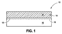
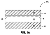
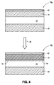
図1を参照すると、強誘電体デバイス10の一部が示されている。デバイス10は、強誘電体材料16上に電極14を備える。強誘電体材料は、1つ以上の酸化物を備えることができ、そして、デバイス10の製造中に起こり得る問題は、電極14と強誘電体材料16との間の界面に沿って、酸素空孔が導入される可能性があることである。このような酸素空孔は、例えば、強誘電体材料の上側の電極14の形成時に導入された欠陥に起因する可能性がある。いくつかの実施形態では、強誘電体材料16の上部領域に沿って、半導体富化領域18が与えられる。その半導体富化領域は、例えば、シリコン、ゲルマニウムなどのうちの1つ以上を備えることができる。その半導体富化領域の下側境界は、破線19を用いて図示されている。いくつかの実施形態では、その半導体富化領域は、非常に薄くすることができ、そして、(図2及び図4の実施例の方法で説明されるように)電極14から下方に又はそれを通って、又は(図3の実施例の方法で説明されるように)半導体含有層から下方に、半導体材料を拡散させることによって形成されるようにすることができる。強誘電体材料16は電気的に絶縁性であるようにすることができる。
Claims (41)
- 電極に隣接する強誘電体材料と、
前記電極に最も近い前記強誘電体材料の表面に沿った半導体材料含有領域であって、前記半導体材料含有領域は前記強誘電体材料の残りの領域よりも高濃度の半導体材料を有するものと、
を備える強誘電体デバイス。 - 前記強誘電体材料は電気的に絶縁性である、請求項1に記載の強誘電体デバイス。
- 前記半導体材料はシリコンを備える、請求項2に記載の強誘電体デバイス。
- 前記半導体材料はゲルマニウムを備える、請求項2に記載の強誘電体デバイス。
- 前記半導体材料はシリコン及びゲルマニウムを備える、請求項2に記載の強誘電体デバイス。
- 前記電極と前記強誘電体材料の間に前記半導体材料の層を備え、前記半導体材料含有領域は前記層に沿っている、請求項2に記載の強誘電体デバイス。
- 前記電極の全体にわたって拡散された前記半導体材料を備え、前記半導体材料含有領域は前記電極に直接面する、請求項2に記載の強誘電体デバイス。
- 前記電極の前記強誘電体材料とは反対側に前記半導体材料の層を更に備える、請求項7に記載の強誘電体デバイス。
- 前記強誘電体デバイスはキャパシタであり、前記電極は、互いに前記強誘電体材料の反対側にある一対の電極のうちの1つである、請求項2に記載の強誘電体デバイス。
- 請求項8に記載のキャパシタを複数の実質的に同一のキャパシタのうちの1つとして備えるメモリアレイ。
- 前記強誘電体デバイスはトランジスタであり、前記電極はトランジスタゲートである、請求項2に記載の強誘電体デバイス。
- 請求項11に記載のトランジスタを複数の実質的に同一のトランジスタの1つとして備えるメモリアレイ。
- 一対の電極間にある酸化物含有絶縁性強誘電体材料と、
前記電極のうちの1つに隣接する前記酸化物含有絶縁性強誘電体材料の半導体材料富化部分と、
を備える強誘電体キャパシタ。 - 前記半導体材料はシリコンを備える、請求項13に記載の強誘電体キャパシタ。
- 前記半導体材料はゲルマニウムを備える、請求項13に記載の強誘電体キャパシタ。
- 前記半導体材料はシリコン及びゲルマニウムを備える、請求項13に記載の強誘電体キャパシタ。
- 前記電極と前記酸化物含有絶縁性強誘電体材料との間に前記半導体材料の層を含み、前記半導体材料富化部分が前記層に沿っている、請求項13に記載の強誘電体キャパシタ。
- 前記電極のうちの1つの全体にわたって拡散された前記半導体材料を備え、前記半導体材料富化部分は前記電極に直接面する、請求項13に記載の強誘電体キャパシタ。
- 前記電極のうちの1つの前記酸化物含有絶縁性強誘電体材料とは反対側に前記半導体材料の層を更に備える、請求項18に記載の強誘電体キャパシタ。
- 前記酸化物含有絶縁性強誘電体材料は、遷移金属酸化物、酸化ジルコニウム、酸化ハフニウム、チタン酸ジルコン酸鉛、酸化タンタル、及びチタン酸バリウムストロンチウムの1つ以上を含み、シリコン、アルミニウム、ランタン、イットリウム、エルビウム、カルシウム、マグネシウム、ニオブ、ストロンチウム、希土類元素、及びそれらの混合物からなる群から選択されるドーパントを有する、請求項13に記載の強誘電体キャパシタ。
- 第1の電極と、
前記第1の電極の上側の絶縁性強誘電体材料と、
前記絶縁性強誘電体材料の上側の前記絶縁性強誘電体材料に直接面する第2の電極であって、前記第2の電極は金属及びシリコンを備えるものと、
前記第2の電極に直接面する前記絶縁性強誘電体材料のシリコン富化領域と、
を備える強誘電体キャパシタ。 - 前記第2の電極は、チタン、タンタル、ハフニウム、タングステン、及びルテニウムの1つ以上と一緒にシリコンを備える、請求項21に記載の強誘電体キャパシタ。
- 前記第2の電極はまた窒素をも備える、請求項22に記載の強誘電体キャパシタ。
- 前記絶縁性強誘電体材料は、酸化ハフニウム及び酸化ジルコニウムの一方又は両方を備える、請求項21に記載の強誘電体キャパシタ。
- 第1の電極と
前記第1の電極の上側の強誘電体材料と、
前記強誘電体材料の上側の前記強誘電体材料に直接面するシリコン含有層と、
前記シリコン含有層の上側の前記シリコン含有層に直接面する第2の電極であって、前記第2の電極は金属を備えるものと、
を備える強誘電体キャパシタ。 - 前記強誘電体材料は電気的に絶縁性である、請求項25に記載の強誘電体キャパシタ。
- 前記シリコン含有層は、少なくとも約1単分子層から約100Å以下の範囲内の厚さを有する、請求項26に記載の強誘電体キャパシタ。
- 前記第2の電極は少なくとも1つの金属窒化物を備える、請求項26に記載の強誘電体キャパシタ。
- 前記第2の電極は、窒化ハフニウム、窒化タングステン、窒化ルテニウム、窒化チタン、及び窒化タンタルのうちの1つ以上を備える、請求項26に記載の強誘電体キャパシタ。
- 第1の電極と、
前記第1の電極の上側の絶縁性強誘電体材料と、
前記絶縁性強誘電体材料の上側の前記絶縁性強誘電体材料に直接面する第2の電極であって、前記第2の電極は金属及びシリコンを備え、前記第2の電極は約5Åから約100Åの範囲内の厚さを有するものと、
前記第2の電極の上側の前記第2の電極に直接面するシリコン含有材料と、
前記第2の電極に直接面する前記絶縁性強誘電体材料のシリコン富化領域と、
を備える強誘電体キャパシタ。 - 前記第2の電極は少なくとも1つの金属窒化物を備える、請求項30に記載の強誘電体キャパシタ。
- 前記第2の電極は、窒化チタン及び窒化タンタルの一方又は両方を備える、請求項30に記載の強誘電体キャパシタ。
- 前記シリコン含有材料はシリコンからなる、請求項30に記載の強誘電体キャパシタ。
- 前記シリコン含有材料は、少なくとも約5Åから約500Å以下の範囲内の厚さを有する、請求項33に記載の強誘電体キャパシタ。
- 第1の電極の上側に酸化物含有強誘電体材料を形成し、
前記酸化物含有強誘電体材料の上側に第2の電極を形成し、
前記第2の電極に隣接して前記酸化物含有強誘電体材料の半導体材料富化部分を形成する、
ことを備える強誘電体キャパシタを形成する方法。 - 前記半導体材料は、シリコン及びゲルマニウムの一方又は両方を備える、請求項35に記載の方法。
- 前記酸化物含有強誘電体材料の前記半導体材料富化部分は、前記第2の電極を形成する前に形成される、請求項35に記載の方法。
- 前記酸化物含有強誘電体材料の前記半導体材料富化部分は、前記第2の電極を形成する前に、前記酸化物含有強誘電体材料の上側に与えられる前記半導体材料の層を用いて形成される、請求項37に記載の方法。
- 前記酸化物含有強誘電体材料の前記半導体材料富化部分は、前記第2の電極を形成した後に形成される、請求項35に記載の方法。
- 前記第2の電極は、その全体にわたって拡散された前記半導体材料を含むように形成され、半導体材料が前記第2の電極から移動して前記半導体材料富化部分を形成する、請求項39に記載の方法。
- 前記第2の電極の前記酸化物含有強誘電体材料とは反対側に前記半導体材料の層を形成し、前記半導体材料富化部分を形成するために前記層から前記第2の電極を通して半導体材料を拡散させる、ことを更に備える、請求項39に記載の方法。
Applications Claiming Priority (3)
| Application Number | Priority Date | Filing Date | Title |
|---|---|---|---|
| US15/164,749 US20170345831A1 (en) | 2016-05-25 | 2016-05-25 | Ferroelectric Devices and Methods of Forming Ferroelectric Devices |
| US15/164,749 | 2016-05-25 | ||
| PCT/US2017/012864 WO2017204863A1 (en) | 2016-05-25 | 2017-01-10 | Ferroelectric devices and methods of forming ferroelectric devices |
Publications (2)
| Publication Number | Publication Date |
|---|---|
| JP2019517153A true JP2019517153A (ja) | 2019-06-20 |
| JP6780026B2 JP6780026B2 (ja) | 2020-11-04 |
Family
ID=60412845
Family Applications (1)
| Application Number | Title | Priority Date | Filing Date |
|---|---|---|---|
| JP2018561674A Active JP6780026B2 (ja) | 2016-05-25 | 2017-01-10 | 強誘電体デバイス及びその形成方法 |
Country Status (7)
| Country | Link |
|---|---|
| US (2) | US20170345831A1 (ja) |
| EP (1) | EP3479413A4 (ja) |
| JP (1) | JP6780026B2 (ja) |
| KR (1) | KR102185788B1 (ja) |
| CN (1) | CN109196654B (ja) |
| TW (1) | TWI661538B (ja) |
| WO (1) | WO2017204863A1 (ja) |
Cited By (1)
| Publication number | Priority date | Publication date | Assignee | Title |
|---|---|---|---|---|
| JP2021520629A (ja) * | 2018-04-02 | 2021-08-19 | ラム リサーチ コーポレーションLam Research Corporation | 窒化ハフニウム層による酸化ハフニウムの強誘電特性の変更 |
Families Citing this family (42)
| Publication number | Priority date | Publication date | Assignee | Title |
|---|---|---|---|---|
| KR20180111303A (ko) * | 2017-03-31 | 2018-10-11 | 에스케이하이닉스 주식회사 | 강유전성 메모리 장치 및 그 제조 방법 |
| US10038092B1 (en) * | 2017-05-24 | 2018-07-31 | Sandisk Technologies Llc | Three-level ferroelectric memory cell using band alignment engineering |
| CN109087997A (zh) * | 2017-06-14 | 2018-12-25 | 萨摩亚商费洛储存科技股份有限公司 | 铁电膜层的制造方法、铁电隧道结单元、存储器元件及其写入与读取方法 |
| US10734531B2 (en) * | 2017-06-22 | 2020-08-04 | The Penn State Research Foundation | Two-dimensional electrostrictive field effect transistor (2D-EFET) |
| KR20190008047A (ko) * | 2017-07-14 | 2019-01-23 | 에스케이하이닉스 주식회사 | 강유전성 메모리 소자 |
| US10930751B2 (en) | 2017-12-15 | 2021-02-23 | Micron Technology, Inc. | Ferroelectric assemblies |
| KR102433290B1 (ko) * | 2018-02-08 | 2022-08-17 | 에스케이하이닉스 주식회사 | 강유전성 소자의 제조 방법 |
| US10702940B2 (en) | 2018-08-20 | 2020-07-07 | Samsung Electronics Co., Ltd. | Logic switching device and method of manufacturing the same |
| KR102693426B1 (ko) | 2018-08-20 | 2024-08-09 | 삼성전자주식회사 | 전자 소자 및 그 제조방법 |
| US10998338B2 (en) * | 2018-11-13 | 2021-05-04 | Micron Technology, Inc. | Integrated assemblies having ferroelectric transistors with heterostructure active regions |
| KR102620866B1 (ko) * | 2018-12-27 | 2024-01-04 | 에스케이하이닉스 주식회사 | 강유전층 및 비-강유전층을 포함하는 유전층 구조물을 구비하는 반도체 소자 |
| US10998025B2 (en) | 2019-02-27 | 2021-05-04 | Kepler Computing, Inc. | High-density low voltage non-volatile differential memory bit-cell with shared plate-line |
| US11476261B2 (en) | 2019-02-27 | 2022-10-18 | Kepler Computing Inc. | High-density low voltage non-volatile memory with unidirectional plate-line and bit-line and pillar capacitor |
| CN109920848A (zh) * | 2019-03-18 | 2019-06-21 | 西安电子科技大学 | 无界面层的ZrO2基反铁电存储器 |
| KR102737493B1 (ko) * | 2019-05-13 | 2024-12-04 | 삼성전자주식회사 | 강유전체를 포함하는 강유전성 반도체 소자 및 그 제조 방법 |
| KR102944584B1 (ko) | 2019-09-18 | 2026-03-25 | 삼성전자주식회사 | 전자 소자 및 그 제조방법 |
| US11527646B2 (en) | 2019-09-24 | 2022-12-13 | Samsung Electronics Co., Ltd. | Domain switching devices and methods of manufacturing the same |
| KR102892295B1 (ko) | 2019-12-23 | 2025-11-26 | 삼성전자주식회사 | 전자 소자 및 그 제조방법 |
| KR102903263B1 (ko) | 2019-12-30 | 2025-12-22 | 삼성전자주식회사 | 강유전성의 커패시터, 트랜지스터, 메모리 소자 및 강유전성의 커패시터의 제조방법 |
| US11087843B1 (en) * | 2020-02-10 | 2021-08-10 | Taiwan Semiconductor Manufacturing Co., Ltd. | Memory with FRAM and SRAM of IC and method for accessing memory |
| KR102906608B1 (ko) * | 2020-05-19 | 2025-12-30 | 삼성전자주식회사 | 산화물 반도체 트랜지스터 |
| US11581335B2 (en) * | 2020-06-23 | 2023-02-14 | Taiwan Semiconductor Manufacturing Company Limited | Ferroelectric tunnel junction devices with metal-FE interface layer and methods for forming the same |
| US12563973B2 (en) | 2020-06-26 | 2026-02-24 | SanDisk Technologies, Inc. | Bonded memory devices and methods of making the same |
| US11903218B2 (en) | 2020-06-26 | 2024-02-13 | Sandisk Technologies Llc | Bonded memory devices and methods of making the same |
| WO2021262239A1 (en) * | 2020-06-26 | 2021-12-30 | Sandisk Technologies Llc | Bonded memory devices and methods of making the same |
| US12362301B2 (en) | 2020-06-26 | 2025-07-15 | SanDisk Technologies, Inc. | Bonded memory devices and methods of making the same |
| CN112271255B (zh) * | 2020-10-23 | 2023-06-09 | 湘潭大学 | 一种铁电电容器和存储单元及其制备方法 |
| US12382640B2 (en) * | 2020-10-30 | 2025-08-05 | Taiwan Semiconductor Manufacturing Company, Ltd. | Memory device and method for fabricating the same |
| US12382670B2 (en) * | 2020-11-04 | 2025-08-05 | Samsung Electronics Co., Ltd. | Thin film structure and semiconductor device comprising the same |
| US12137572B2 (en) * | 2021-02-26 | 2024-11-05 | Taiwan Semiconductor Manufacturing Company, Ltd. | Ferroelectric memory device and method of manufacturing the same |
| WO2022190817A1 (ja) * | 2021-03-11 | 2022-09-15 | 国立大学法人東京工業大学 | 強誘電性薄膜の形成方法、それを備える半導体装置 |
| US11843037B2 (en) | 2021-03-19 | 2023-12-12 | Samsung Electronics Co., Ltd. | Semiconductor device and method of manufacturing the semiconductor device |
| US11527277B1 (en) | 2021-06-04 | 2022-12-13 | Kepler Computing Inc. | High-density low voltage ferroelectric memory bit-cell |
| KR20230048967A (ko) * | 2021-10-05 | 2023-04-12 | 에스케이하이닉스 주식회사 | 에피택셜 층인 전극층과 유전 구조물을 포함하는 반도체 장치 |
| KR20230055239A (ko) | 2021-10-18 | 2023-04-25 | 에스케이하이닉스 주식회사 | 강유전체 메모리 장치 및 이의 제조 방법 |
| US11729995B1 (en) | 2021-11-01 | 2023-08-15 | Kepler Computing Inc. | Common mode compensation for non-linear polar material 1TnC memory bit-cell |
| US11482270B1 (en) | 2021-11-17 | 2022-10-25 | Kepler Computing Inc. | Pulsing scheme for a ferroelectric memory bit-cell to minimize read or write disturb effect and refresh logic |
| US12108609B1 (en) | 2022-03-07 | 2024-10-01 | Kepler Computing Inc. | Memory bit-cell with stacked and folded planar capacitors |
| CN116847660A (zh) * | 2022-03-22 | 2023-10-03 | 华为技术有限公司 | 一种铁电材料、铁电存储单元、存储器及电子设备 |
| US20230395134A1 (en) | 2022-06-03 | 2023-12-07 | Kepler Computing Inc. | Write disturb mitigation for non-linear polar material based multi-capacitor bit-cell |
| US12347476B1 (en) | 2022-12-27 | 2025-07-01 | Kepler Computing Inc. | Apparatus and method to improve sensing noise margin in a non-linear polar material based bit-cell |
| US12334127B2 (en) | 2023-01-30 | 2025-06-17 | Kepler Computing Inc. | Non-linear polar material based multi-capacitor high density bit-cell |
Citations (4)
| Publication number | Priority date | Publication date | Assignee | Title |
|---|---|---|---|---|
| JPH06196654A (ja) * | 1992-08-07 | 1994-07-15 | Samsung Electron Co Ltd | 半導体メモリ装置及びその製造方法 |
| JP2005209722A (ja) * | 2004-01-20 | 2005-08-04 | Seiko Epson Corp | 強誘電体膜、強誘電体メモリ、及び圧電素子 |
| JP2014053568A (ja) * | 2012-09-10 | 2014-03-20 | Toshiba Corp | 強誘電体メモリ及びその製造方法 |
| US20160064228A1 (en) * | 2014-08-28 | 2016-03-03 | Globalfoundries Inc. | Method of forming a semiconductor structure including a ferroelectric material and semiconductor structure including a ferroelectric transistor |
Family Cites Families (26)
| Publication number | Priority date | Publication date | Assignee | Title |
|---|---|---|---|---|
| US4745278A (en) * | 1986-10-23 | 1988-05-17 | Varo, Inc. | Capacitive bolometer with improved responsivity |
| US5825609A (en) * | 1996-04-23 | 1998-10-20 | International Business Machines Corporation | Compound electrode stack capacitor |
| KR100224729B1 (ko) * | 1996-12-10 | 1999-10-15 | 윤종용 | 반도체장치의 강유전체 커패시터 및 그 제조방법 |
| AU1649797A (en) * | 1997-03-13 | 1998-09-17 | Christopher John Ball | Self-watering plant guard |
| US6610548B1 (en) * | 1999-03-26 | 2003-08-26 | Sony Corporation | Crystal growth method of oxide, cerium oxide, promethium oxide, multi-layered structure of oxides, manufacturing method of field effect transistor, manufacturing method of ferroelectric non-volatile memory and ferroelectric non-volatile memory |
| US6236076B1 (en) * | 1999-04-29 | 2001-05-22 | Symetrix Corporation | Ferroelectric field effect transistors for nonvolatile memory applications having functional gradient material |
| US6297527B1 (en) * | 1999-05-12 | 2001-10-02 | Micron Technology, Inc. | Multilayer electrode for ferroelectric and high dielectric constant capacitors |
| US8253183B2 (en) * | 2001-06-28 | 2012-08-28 | Samsung Electronics Co., Ltd. | Charge trapping nonvolatile memory devices with a high-K blocking insulation layer |
| KR100388465B1 (ko) * | 2001-06-30 | 2003-06-25 | 주식회사 하이닉스반도체 | 루테늄 하부전극을 갖는 강유전체 캐패시터 및 그 형성방법 |
| US6489645B1 (en) * | 2001-07-03 | 2002-12-03 | Matsushita Electric Industrial Co., Ltd. | Integrated circuit device including a layered superlattice material with an interface buffer layer |
| JP3986859B2 (ja) * | 2002-03-25 | 2007-10-03 | 富士通株式会社 | 薄膜キャパシタ及びその製造方法 |
| JP3932356B2 (ja) * | 2002-07-22 | 2007-06-20 | 国立大学法人東北大学 | 不揮発性固体磁気メモリの記録方法 |
| US6774446B2 (en) * | 2002-10-31 | 2004-08-10 | Hewlett-Packard Development Company, L.P. | Efficient spin-injection into semiconductors |
| US8182719B2 (en) * | 2003-06-11 | 2012-05-22 | Yeda Research And Development Company Ltd. | Pyroelectric compound and method of its preparation |
| KR100785458B1 (ko) * | 2005-05-18 | 2007-12-13 | 삼성전자주식회사 | 강유전체 박막의 제조 방법 및 이를 이용한 반도체 장치의제조 방법 |
| JP5054936B2 (ja) * | 2005-06-22 | 2012-10-24 | パナソニック株式会社 | 電気機械メモリ、それを用いた電気回路及び電気機械メモリの駆動方法 |
| JP2009117768A (ja) * | 2007-11-09 | 2009-05-28 | Toshiba Corp | 半導体記憶装置およびその製造方法 |
| KR101096203B1 (ko) * | 2010-04-08 | 2011-12-22 | 주식회사 하이닉스반도체 | 반도체 장치 및 그 제조방법 |
| JP2012256702A (ja) * | 2011-06-08 | 2012-12-27 | Rohm Co Ltd | 強誘電体キャパシタ |
| US8637413B2 (en) * | 2011-12-02 | 2014-01-28 | Sandisk 3D Llc | Nonvolatile resistive memory element with a passivated switching layer |
| JP6008365B2 (ja) * | 2012-09-05 | 2016-10-19 | 新電元工業株式会社 | 充電装置 |
| JP5902111B2 (ja) * | 2013-03-06 | 2016-04-13 | 株式会社東芝 | 半導体記憶装置 |
| KR101609178B1 (ko) * | 2013-09-16 | 2016-04-07 | 엔에이치엔엔터테인먼트 주식회사 | 사용자의 이동경로에 기반하여 보상을 제공하는 서비스 방법 및 시스템 |
| JP6062552B2 (ja) * | 2014-03-17 | 2017-01-18 | 株式会社東芝 | 不揮発性記憶装置 |
| US9147689B1 (en) * | 2014-04-16 | 2015-09-29 | Micron Technology, Inc. | Methods of forming ferroelectric capacitors |
| US9768181B2 (en) * | 2014-04-28 | 2017-09-19 | Micron Technology, Inc. | Ferroelectric memory and methods of forming the same |
-
2016
- 2016-05-25 US US15/164,749 patent/US20170345831A1/en not_active Abandoned
-
2017
- 2017-01-10 KR KR1020187036277A patent/KR102185788B1/ko active Active
- 2017-01-10 JP JP2018561674A patent/JP6780026B2/ja active Active
- 2017-01-10 WO PCT/US2017/012864 patent/WO2017204863A1/en not_active Ceased
- 2017-01-10 CN CN201780032702.XA patent/CN109196654B/zh active Active
- 2017-01-10 EP EP17803184.5A patent/EP3479413A4/en active Pending
- 2017-02-03 TW TW106103645A patent/TWI661538B/zh active
-
2020
- 2020-03-30 US US16/834,666 patent/US20200227423A1/en not_active Abandoned
Patent Citations (4)
| Publication number | Priority date | Publication date | Assignee | Title |
|---|---|---|---|---|
| JPH06196654A (ja) * | 1992-08-07 | 1994-07-15 | Samsung Electron Co Ltd | 半導体メモリ装置及びその製造方法 |
| JP2005209722A (ja) * | 2004-01-20 | 2005-08-04 | Seiko Epson Corp | 強誘電体膜、強誘電体メモリ、及び圧電素子 |
| JP2014053568A (ja) * | 2012-09-10 | 2014-03-20 | Toshiba Corp | 強誘電体メモリ及びその製造方法 |
| US20160064228A1 (en) * | 2014-08-28 | 2016-03-03 | Globalfoundries Inc. | Method of forming a semiconductor structure including a ferroelectric material and semiconductor structure including a ferroelectric transistor |
Non-Patent Citations (1)
| Title |
|---|
| BOESCKE, T. S. ET AL.: "Phase transitions in ferroelectric silicon doped hafnium oxide", APPLIED PHYSICS LETTERS, vol. 99, JPN7020000559, 15 September 2011 (2011-09-15), pages 112904 - 1, ISSN: 0004223276 * |
Cited By (2)
| Publication number | Priority date | Publication date | Assignee | Title |
|---|---|---|---|---|
| JP2021520629A (ja) * | 2018-04-02 | 2021-08-19 | ラム リサーチ コーポレーションLam Research Corporation | 窒化ハフニウム層による酸化ハフニウムの強誘電特性の変更 |
| JP7307745B2 (ja) | 2018-04-02 | 2023-07-12 | ラム リサーチ コーポレーション | 窒化ハフニウム層による酸化ハフニウムの強誘電特性の変更 |
Also Published As
| Publication number | Publication date |
|---|---|
| TWI661538B (zh) | 2019-06-01 |
| EP3479413A1 (en) | 2019-05-08 |
| KR102185788B1 (ko) | 2020-12-03 |
| CN109196654B (zh) | 2022-09-30 |
| TW201742235A (zh) | 2017-12-01 |
| US20170345831A1 (en) | 2017-11-30 |
| US20200227423A1 (en) | 2020-07-16 |
| WO2017204863A1 (en) | 2017-11-30 |
| JP6780026B2 (ja) | 2020-11-04 |
| EP3479413A4 (en) | 2019-10-23 |
| KR20180137580A (ko) | 2018-12-27 |
| CN109196654A (zh) | 2019-01-11 |
Similar Documents
| Publication | Publication Date | Title |
|---|---|---|
| CN109196654B (zh) | 铁电装置及形成铁电装置的方法 | |
| US11856790B2 (en) | Ferroelectric capacitors | |
| US10784374B2 (en) | Recessed transistors containing ferroelectric material | |
| TWI834276B (zh) | 記憶體胞元及形成包含具有不同總電阻之電流洩漏路徑之電容器之方法 | |
| US12302623B2 (en) | Ferroelectric assemblies and methods of forming ferroelectric assemblies | |
| KR20250133323A (ko) | 커패시터들의 어레이, 메모리 셀들의 어레이, 및 커패시터들의 어레이 형성에 사용되는 방법 | |
| WO2023161755A1 (ja) | 記憶装置 |
Legal Events
| Date | Code | Title | Description |
|---|---|---|---|
| A521 | Request for written amendment filed |
Free format text: JAPANESE INTERMEDIATE CODE: A523 Effective date: 20190201 |
|
| A621 | Written request for application examination |
Free format text: JAPANESE INTERMEDIATE CODE: A621 Effective date: 20190201 |
|
| A977 | Report on retrieval |
Free format text: JAPANESE INTERMEDIATE CODE: A971007 Effective date: 20200220 |
|
| A131 | Notification of reasons for refusal |
Free format text: JAPANESE INTERMEDIATE CODE: A131 Effective date: 20200303 |
|
| A521 | Request for written amendment filed |
Free format text: JAPANESE INTERMEDIATE CODE: A523 Effective date: 20200602 |
|
| RD03 | Notification of appointment of power of attorney |
Free format text: JAPANESE INTERMEDIATE CODE: A7423 Effective date: 20200602 |
|
| TRDD | Decision of grant or rejection written | ||
| A01 | Written decision to grant a patent or to grant a registration (utility model) |
Free format text: JAPANESE INTERMEDIATE CODE: A01 Effective date: 20200915 |
|
| A61 | First payment of annual fees (during grant procedure) |
Free format text: JAPANESE INTERMEDIATE CODE: A61 Effective date: 20201014 |
|
| R150 | Certificate of patent or registration of utility model |
Ref document number: 6780026 Country of ref document: JP Free format text: JAPANESE INTERMEDIATE CODE: R150 |
|
| R250 | Receipt of annual fees |
Free format text: JAPANESE INTERMEDIATE CODE: R250 |
|
| R250 | Receipt of annual fees |
Free format text: JAPANESE INTERMEDIATE CODE: R250 |
|
| R250 | Receipt of annual fees |
Free format text: JAPANESE INTERMEDIATE CODE: R250 |