JP2019523402A - DETECTOR MODULE, DETECTOR, IMAGING DEVICE AND DETECTOR MODULE MANUFACTURING METHOD - Google Patents
DETECTOR MODULE, DETECTOR, IMAGING DEVICE AND DETECTOR MODULE MANUFACTURING METHOD Download PDFInfo
- Publication number
- JP2019523402A JP2019523402A JP2019500891A JP2019500891A JP2019523402A JP 2019523402 A JP2019523402 A JP 2019523402A JP 2019500891 A JP2019500891 A JP 2019500891A JP 2019500891 A JP2019500891 A JP 2019500891A JP 2019523402 A JP2019523402 A JP 2019523402A
- Authority
- JP
- Japan
- Prior art keywords
- integrated circuit
- interposer
- direct conversion
- conversion crystal
- detector
- Prior art date
- Legal status (The legal status is an assumption and is not a legal conclusion. Google has not performed a legal analysis and makes no representation as to the accuracy of the status listed.)
- Granted
Links
Images

Classifications
-
- A—HUMAN NECESSITIES
- A61—MEDICAL OR VETERINARY SCIENCE; HYGIENE
- A61B—DIAGNOSIS; SURGERY; IDENTIFICATION
- A61B6/00—Apparatus or devices for radiation diagnosis; Apparatus or devices for radiation diagnosis combined with radiation therapy equipment
- A61B6/02—Arrangements for diagnosis sequentially in different planes; Stereoscopic radiation diagnosis
- A61B6/03—Computed tomography [CT]
- A61B6/032—Transmission computed tomography [CT]
- A61B6/035—Mechanical aspects of CT
-
- G—PHYSICS
- G01—MEASURING; TESTING
- G01T—MEASUREMENT OF NUCLEAR OR X-RADIATION
- G01T1/00—Measuring X-radiation, gamma radiation, corpuscular radiation, or cosmic radiation
- G01T1/16—Measuring radiation intensity
- G01T1/24—Measuring radiation intensity with semiconductor detectors
-
- H—ELECTRICITY
- H10—SEMICONDUCTOR DEVICES; ELECTRIC SOLID-STATE DEVICES NOT OTHERWISE PROVIDED FOR
- H10F—INORGANIC SEMICONDUCTOR DEVICES SENSITIVE TO INFRARED RADIATION, LIGHT, ELECTROMAGNETIC RADIATION OF SHORTER WAVELENGTH OR CORPUSCULAR RADIATION
- H10F39/00—Integrated devices, or assemblies of multiple devices, comprising at least one element covered by group H10F30/00, e.g. radiation detectors comprising photodiode arrays
- H10F39/011—Manufacture or treatment of image sensors covered by group H10F39/12
- H10F39/018—Manufacture or treatment of image sensors covered by group H10F39/12 of hybrid image sensors
-
- H—ELECTRICITY
- H10—SEMICONDUCTOR DEVICES; ELECTRIC SOLID-STATE DEVICES NOT OTHERWISE PROVIDED FOR
- H10F—INORGANIC SEMICONDUCTOR DEVICES SENSITIVE TO INFRARED RADIATION, LIGHT, ELECTROMAGNETIC RADIATION OF SHORTER WAVELENGTH OR CORPUSCULAR RADIATION
- H10F39/00—Integrated devices, or assemblies of multiple devices, comprising at least one element covered by group H10F30/00, e.g. radiation detectors comprising photodiode arrays
- H10F39/10—Integrated devices
- H10F39/12—Image sensors
- H10F39/18—Complementary metal-oxide-semiconductor [CMOS] image sensors; Photodiode array image sensors
- H10F39/189—X-ray, gamma-ray or corpuscular radiation imagers
- H10F39/1892—Direct radiation image sensors
-
- H—ELECTRICITY
- H10—SEMICONDUCTOR DEVICES; ELECTRIC SOLID-STATE DEVICES NOT OTHERWISE PROVIDED FOR
- H10F—INORGANIC SEMICONDUCTOR DEVICES SENSITIVE TO INFRARED RADIATION, LIGHT, ELECTROMAGNETIC RADIATION OF SHORTER WAVELENGTH OR CORPUSCULAR RADIATION
- H10F39/00—Integrated devices, or assemblies of multiple devices, comprising at least one element covered by group H10F30/00, e.g. radiation detectors comprising photodiode arrays
- H10F39/10—Integrated devices
- H10F39/12—Image sensors
- H10F39/18—Complementary metal-oxide-semiconductor [CMOS] image sensors; Photodiode array image sensors
- H10F39/189—X-ray, gamma-ray or corpuscular radiation imagers
- H10F39/1895—X-ray, gamma-ray or corpuscular radiation imagers of the hybrid type
-
- H—ELECTRICITY
- H10—SEMICONDUCTOR DEVICES; ELECTRIC SOLID-STATE DEVICES NOT OTHERWISE PROVIDED FOR
- H10F—INORGANIC SEMICONDUCTOR DEVICES SENSITIVE TO INFRARED RADIATION, LIGHT, ELECTROMAGNETIC RADIATION OF SHORTER WAVELENGTH OR CORPUSCULAR RADIATION
- H10F39/00—Integrated devices, or assemblies of multiple devices, comprising at least one element covered by group H10F30/00, e.g. radiation detectors comprising photodiode arrays
- H10F39/80—Constructional details of image sensors
- H10F39/804—Containers or encapsulations
-
- H—ELECTRICITY
- H10—SEMICONDUCTOR DEVICES; ELECTRIC SOLID-STATE DEVICES NOT OTHERWISE PROVIDED FOR
- H10F—INORGANIC SEMICONDUCTOR DEVICES SENSITIVE TO INFRARED RADIATION, LIGHT, ELECTROMAGNETIC RADIATION OF SHORTER WAVELENGTH OR CORPUSCULAR RADIATION
- H10F39/00—Integrated devices, or assemblies of multiple devices, comprising at least one element covered by group H10F30/00, e.g. radiation detectors comprising photodiode arrays
- H10F39/80—Constructional details of image sensors
- H10F39/809—Constructional details of image sensors of hybrid image sensors
-
- H—ELECTRICITY
- H10—SEMICONDUCTOR DEVICES; ELECTRIC SOLID-STATE DEVICES NOT OTHERWISE PROVIDED FOR
- H10F—INORGANIC SEMICONDUCTOR DEVICES SENSITIVE TO INFRARED RADIATION, LIGHT, ELECTROMAGNETIC RADIATION OF SHORTER WAVELENGTH OR CORPUSCULAR RADIATION
- H10F39/00—Integrated devices, or assemblies of multiple devices, comprising at least one element covered by group H10F30/00, e.g. radiation detectors comprising photodiode arrays
- H10F39/80—Constructional details of image sensors
- H10F39/811—Interconnections
Landscapes
- Health & Medical Sciences (AREA)
- Life Sciences & Earth Sciences (AREA)
- Engineering & Computer Science (AREA)
- High Energy & Nuclear Physics (AREA)
- Molecular Biology (AREA)
- Physics & Mathematics (AREA)
- Medical Informatics (AREA)
- Radiology & Medical Imaging (AREA)
- Surgery (AREA)
- Nuclear Medicine, Radiotherapy & Molecular Imaging (AREA)
- Optics & Photonics (AREA)
- Pathology (AREA)
- Theoretical Computer Science (AREA)
- Biomedical Technology (AREA)
- Heart & Thoracic Surgery (AREA)
- Pulmonology (AREA)
- Biophysics (AREA)
- Animal Behavior & Ethology (AREA)
- General Health & Medical Sciences (AREA)
- Public Health (AREA)
- Veterinary Medicine (AREA)
- General Physics & Mathematics (AREA)
- Spectroscopy & Molecular Physics (AREA)
- Measurement Of Radiation (AREA)
- Solid State Image Pick-Up Elements (AREA)
- Light Receiving Elements (AREA)
Abstract
本発明は、検出器モジュールに関し、検出器モジュールは、入射光子を電気信号に変換する直接変換結晶10であって、第1の表面上に堆積されるカソードメタライゼーション100及び第2の表面上に堆積されるアノードメタライゼーション101を有する、直接変換結晶と、前記直接変換結晶と電気的に通信する集積回路(12)であって、前記集積回路が前記直接変換結晶より小さい幅を有し、それにより前記集積回路の側面に幅方向の凹部120を形成する、集積回路と、前記直接変換結晶と前記集積回路との間に配置され、前記直接変換結晶と前記集積回路との間の電気通信を提供するインタポーザ11、11aであって、前記集積回路に面した、前記直接変換結晶のアノードメタライゼーション101と接着され、はんだ付けされ、又は接合される別個の素子として形成されるインタポーザ11、11aと、複数のケーブルを提供するマルチリードフレックスケーブル13、13a、13b、13c、13dであって、マルチリードフレックスケーブルは、一方の面が前記直接変換結晶に接続され、他方の面が前記集積回路12に接続される第1の部分131、131a、131b、131c、131d、及び第1の部分に対し曲げられ及び前記凹部内に配される第2の部分131を有する、マルチリードフレックスケーブルと、を有する。The present invention relates to a detector module, which is a direct conversion crystal 10 that converts incident photons into an electrical signal, on the cathode metallization 100 and the second surface deposited on the first surface. A direct conversion crystal having an anode metallization 101 deposited thereon and an integrated circuit (12) in electrical communication with said direct conversion crystal, said integrated circuit having a width smaller than said direct conversion crystal, Forming an indentation 120 in a width direction on a side surface of the integrated circuit, disposed between the integrated circuit, the direct conversion crystal, and the integrated circuit, and performing electrical communication between the direct conversion crystal and the integrated circuit. An interposer 11, 11 a to be provided, which is bonded and soldered to the anode metallization 101 of the direct conversion crystal facing the integrated circuit Or interposers 11, 11a formed as separate elements to be joined and multi-lead flex cables 13, 13a, 13b, 13c, 13d providing a plurality of cables, the multi-lead flex cables being on one side Is connected to the direct conversion crystal, and the other surface is bent with respect to the first portion 131, 131a, 131b, 131c, 131d and the first portion connected to the integrated circuit 12, and arranged in the recess. A multi-lead flex cable having a second portion 131 to be provided.
Description
本発明は、検出器モジュール、検出器、イメージング装置、及び検出器モジュールの製造方法に関する。 The present invention relates to a detector module, a detector, an imaging apparatus, and a method for manufacturing the detector module.
4面バッタビリテイ(4-side-buttability、四方隙間のない構造)を有する検出器モジュールは、例えば医療又は工業イメージング用のX線及びCTイメージング装置において使用されるような大面積検出器を構築するために必要不可欠である。エネルギー積分検出器の場合、この問題は、フォトダイオードアレイのアノード接点の、集積回路(一般にASIC)への再配線(redistribution)を提供する(セラミック)インタポーザを使用することによって解決される。この集積回路は、(背面照射される)フォトダイオードアレイよりも小さい。より進歩したアプローチでは、(高価な)セラミックインタポーザが回避されることができるように、再配線機能が、フォトダイオードアレイアノード上に実装される。より進歩したアプローチは、アノードコンタクトとASIC上の対応する入力パッドとの間の短いトラック長をもたらす。トラック長を短くすると、ASICの入力パッドから見た容量性負荷が減るため、ノイズを減らすことができるが、利用可能なアナログ読み出しチャネルは、長いトラック長に起因するSNRに容易に対処することができる。低減される容量性負荷のためSNRが一層高くなるので、トラック長が短いほど、ASICの消費電力を低減することができる。 A detector module with 4-side-buttability (structure with no four-sided gap) is used to construct large area detectors such as those used in medical or industrial imaging X-ray and CT imaging devices. Indispensable to. In the case of an energy integrating detector, this problem is solved by using a (ceramic) interposer that provides redistribution of the anode contacts of the photodiode array to an integrated circuit (typically an ASIC). This integrated circuit is smaller than a photodiode array (back illuminated). In a more advanced approach, a redistribution function is implemented on the photodiode array anode so that (expensive) ceramic interposers can be avoided. More advanced approaches result in shorter track lengths between the anode contact and the corresponding input pad on the ASIC. Shorter track lengths reduce the capacitive load seen from the ASIC input pad, thus reducing noise, but available analog read channels can easily cope with SNR due to longer track lengths. it can. Since the SNR is further increased due to the reduced capacitive load, the shorter the track length, the lower the power consumption of the ASIC.
例えばCTシステムで使用されるような光子計数スペクトル検出器の場合、直接変換結晶(例えばCZT)センサピクセルと読み出しASICの入力パッドとの間の長いトラック長は認容できない。これは、結果的に生じるノイズが、受け入れられない程度にエネルギー分離能力を制限するからである。非常に高速のアナログ増幅器及び単位面積あたり一層多くのピクセル数が、1ピクセルあたりの消費電力を制限するので、エネルギー積分読み出しシステムよりも小さい容量性負荷しか認容できない。しかしながら、更に重要なことに、長いトラックは更に、ピクセルの活動に依存してピクセル間クロストークを引き起こす。 For photon counting spectral detectors, such as those used in CT systems, long track lengths between direct conversion crystal (eg CZT) sensor pixels and readout ASIC input pads are unacceptable. This is because the resulting noise limits the energy separation capability to an unacceptable extent. Very high speed analog amplifiers and a higher number of pixels per unit area limit power consumption per pixel, so that only a smaller capacitive load is acceptable than an energy integrating readout system. More importantly, however, long tracks also cause inter-pixel crosstalk depending on pixel activity.
最小のトラック長を伴って相互接続を提供する直接的なアプローチは、TSV(シリコン貫通ビア)を使用してASICを設計することである。特定の量産品(携帯電話カメラ、スタックメモリ装置など)の場合、TSVは、安価に入手できるが、比較的少ない生産量の高性能医用イメージング装置の場合、TSVは、受け入れ可能な価格で容易に入手できない。更に、TSVの場合、あるピクセル用のエレクトロニクス及びすべてのピクセルに共通のエレクトロニクスが、選ばれたCMOS技術において利用できるすべてのスペースを必要とし得ないとしても、ASICは、センサと同じ大きさでなければならず、したがって、TSVによって提供される背面コンタクトを支援するためだけに、高価なダイ面積が或る程度消費されうる。最後に、ASICを機械的にロバスト(アセンブルの最中、有用である)にするようTSVに関して十分な厚さのASICを得るために、TSV処理はCMOS処理の後に行う必要があり、これは、多くの場合、二次サプライヤを必要とする。 A direct approach to providing interconnects with minimum track length is to design ASICs using TSVs (Through Silicon Vias). For certain mass-produced products (cell phone cameras, stack memory devices, etc.), TSVs are available inexpensively, but for high-performance medical imaging devices with relatively low production volumes, TSVs are easily available at an acceptable price. Not available. Furthermore, in the case of TSV, the ASIC must be the same size as the sensor, even though the electronics for one pixel and the electronics common to all pixels may not require all the space available in the chosen CMOS technology. Therefore, some expensive die area can be consumed only to support the back contact provided by the TSV. Finally, in order to obtain an ASIC that is sufficiently thick with respect to TSV to make the ASIC mechanically robust (useful during assembly), the TSV process must be performed after the CMOS process, Often you need a secondary supplier.
米国特許出願公開第2010/327173A1号公報は、入射光子を電気信号に変換するための直接変換結晶であって、第1の表面上に堆積されたアノード層と第2の表面上に堆積されたカソード層とを有する直接変換結晶と、アノード層上に堆積され、直接変換結晶のパッドアレイレイアウトを所定のリードパターンに適合させるよう構成される再配線層と、直接変換結晶と電気的に通信する集積回路と、再配線層に接続され、イメージングモジュールと他の相互接続レベルとの間の接続を提供する複数の入力/出力電気経路と、を有する検出器モジュールを開示している。フレックスピッグテールは、再配線層上の1又は複数の対応する再配線周縁パッドにはんだ付けされ、集積回路のための複数の入力/出力電気経路を提供することができる。 US Patent Application Publication No. 2010 / 327173A1 is a direct conversion crystal for converting incident photons into an electrical signal, deposited on a first surface and an anode layer deposited on a first surface. A direct conversion crystal having a cathode layer, a redistribution layer deposited on the anode layer and configured to adapt the pad array layout of the direct conversion crystal to a predetermined lead pattern, and in electrical communication with the direct conversion crystal A detector module is disclosed having an integrated circuit and a plurality of input / output electrical paths connected to the redistribution layer and providing a connection between the imaging module and other interconnect levels. The flex pigtail can be soldered to one or more corresponding redistribution peripheral pads on the redistribution layer to provide multiple input / output electrical paths for the integrated circuit.
米国特許出願公開第2009/080601A1号公報は、X線を受け取ると電荷を発生するように構成される直接変換材料と、直接変換材料において生成された電荷を収集するように構成される複数の金属化されたアノードと、少なくとも1つの読み出し装置と、複数の金属化されたアノードから少なくとも1つの読み出し装置へ電荷を送るように構成される複数の電気経路を有する再配線層と、を有するCT検出器を開示している。 US Patent Application Publication No. 2009 / 080601A1 discloses a direct conversion material configured to generate charge upon receipt of X-rays and a plurality of metals configured to collect the charge generated in the direct conversion material CT having a structured anode, at least one readout device, and a redistribution layer having a plurality of electrical paths configured to route charge from the plurality of metallized anodes to the at least one readout device A vessel is disclosed.
国際公開第2016/066850A1号公報は、放射線信号を検出するためのセンサ装置を開示している。4面バッタブルの能力を維持しながら高い信号完全性及び費用効果を可能にするために、センサ装置は、複数の検出器を有するセンサアレイと、受信した放射線信号を電気信号に変換するセンサ素子と、第1の側面と第2の側面との間に横方向に延びるインタポーザ素子と、集積素子とを有する。 International Publication No. 2016 / 066850A1 discloses a sensor device for detecting a radiation signal. In order to enable high signal integrity and cost effectiveness while maintaining the capability of a four-sided batter, the sensor device includes a sensor array having a plurality of detectors, and a sensor element that converts the received radiation signal into an electrical signal. And an interposer element extending in the lateral direction between the first side surface and the second side surface, and an integrated element.
本発明の目的は、TSVを使用せずに4面バッタブルを可能にしながらも、安価に製造することができる検出器モジュールを提供することである。本発明のさらなる目的は、検出器、イメージング装置、及び検出器モジュールを製造する方法を提供することである。 It is an object of the present invention to provide a detector module that can be manufactured at low cost while allowing four-sided bubbling without using a TSV. It is a further object of the present invention to provide a method for manufacturing a detector, an imaging device and a detector module.
本発明の第1の態様において、入射光子を電気信号に変換する直接変換結晶であって、第1の表面上に堆積されたカソードメタライゼーション及び第2の表面上に堆積されたアノードメタライゼーションを有する直接変換結晶と、直接変換結晶と電気的に通信する集積回路であって、直接変換結晶よりも小さい幅を有し、それによって集積回路の側面に、幅方向に凹部を形成する集積回路と、直接変換結晶と集積回路との間に配置され、直接変換結晶と集積回路との間の電気通信を提供するインタポーザであって、集積回路に面する直接変換結晶のアノードメタライゼーションと接着され、はんだ付けされ又は接合される個別の素子として設けられるインタポーザと、複数の出力経路を提供するマルチリードフレックスケーブルであって、一方の面が直接変換結晶に接続され、他方の面が集積回路に接続される第1の部分と、第1の部分に対して曲げられ及び凹部内に配置される第2の部分と、を有するマルチリードフレックスケーブルと、を有する検出器モジュールが提示される。 In a first aspect of the invention, a direct conversion crystal that converts incident photons into an electrical signal, comprising a cathode metallization deposited on a first surface and an anode metallization deposited on a second surface. An integrated circuit that is in electrical communication with the direct conversion crystal and has a smaller width than the direct conversion crystal, thereby forming a recess in the width direction on a side surface of the integrated circuit; An interposer disposed between the direct conversion crystal and the integrated circuit and providing electrical communication between the direct conversion crystal and the integrated circuit, adhered to the anode metallization of the direct conversion crystal facing the integrated circuit; An interposer provided as a separate element to be soldered or bonded, and a multi-lead flex cable providing multiple output paths, Having a first portion connected directly to the conversion crystal and a second portion connected to the integrated circuit, and a second portion bent relative to the first portion and disposed in the recess. A detector module having a multi-lead flex cable is presented.
本発明の他の態様において、検出器モジュールの平面アレイを形成するように互いに隣接して配置された本明細書に開示される複数の検出器モジュールを有する検出器が提示される。 In another aspect of the invention, a detector is presented having a plurality of detector modules as disclosed herein disposed adjacent to each other to form a planar array of detector modules.
本発明の他の態様において、本明細書に開示される検出器を有するイメージング装置が提示される。 In another aspect of the present invention, an imaging device having the detector disclosed herein is presented.
本発明の他の態様において、検出器モジュールを製造する方法であって、インタポーザを個別の素子として製作するステップと、入射光子を電気信号に変換するように構成される直接変換結晶のアノードメタライゼーションに、インタポーザを、接着、はんだ付け又は接合によって接触させるステップであって、直接変換結晶は、第1の表面に堆積されたカソードメタライゼーション及び第2の表面に堆積されたアノードメタライゼーションを有する、ステップと、直接変換結晶と反対側のインタポーザの面に集積回路を配置するステップであって、インタポーザは、集積回路と直接変換結晶との間の電気通信を提供し、集積回路の幅は、直接変換結晶の幅より小さく、それにより集積回路の側面に、幅方向の凹部を形成する、ステップと、複数の出力経路を提供するマルチリードフレックスケーブルを凹部内に配置するステップであって、マルチリードフレックスケーブルの第1の部分は、一方の面が直接変換結晶に接続され、他方の面が集積回路の対向する面に配置され、第1部分に対し曲げられる第2部分が、凹部内に配置される、ステップと、を有する方法が提示される。 In another aspect of the present invention, a method of manufacturing a detector module comprising fabricating an interposer as a discrete element and anodic metallization of a direct conversion crystal configured to convert incident photons into an electrical signal A step of contacting the interposer by bonding, soldering or bonding, wherein the direct conversion crystal has a cathode metallization deposited on the first surface and an anode metallization deposited on the second surface; Placing an integrated circuit on the side of the interposer opposite the direct conversion crystal, the interposer providing electrical communication between the integrated circuit and the direct conversion crystal, the width of the integrated circuit being directly Forming a recess in the width direction on the side of the integrated circuit that is smaller than the width of the conversion crystal, and Placing a multi-lead flex cable providing a number of output paths in a recess, wherein a first part of the multi-lead flex cable has one side directly connected to the conversion crystal and the other side is integrated circuit A second portion that is disposed on opposite surfaces of the first portion and that is bent with respect to the first portion is disposed in the recess.
本発明の好適な実施形態は従属請求項に規定される。特許請求の範囲に記載の検出器、イメージング装置、及び方法は、特許請求の範囲に記載の検出器モジュール、特に従属請求項に規定され、本明細書に開示される検出器モジュールと同様の及び/又は同一の好適な実施形態を有する。 Preferred embodiments of the invention are defined in the dependent claims. The detectors, imaging devices and methods described in the claims are similar to the detector modules defined in the claims, in particular those defined in the dependent claims and disclosed herein. And / or having the same preferred embodiment.
本発明の構成要素の1つは、小さい曲げ半径を可能にする細いマルチリードフレックスケーブルである。曲げ半径が小さいため、フレックスケーブルを収容するのに必要なスペースはほんのわずかであり、したがって、フレックスケーブルは、集積回路に形成された凹部内に少なくとも部分的に(すなわちその第2の部分が)配置されることができるので、隣接する検出器モジュール間のスペースを最小にし、又は非常に小さく(例えば200μm)保つことができる。 One component of the present invention is a thin multi-lead flex cable that allows for a small bend radius. Because of the small bend radius, only a small amount of space is required to accommodate the flex cable, and therefore the flex cable is at least partially within the recess formed in the integrated circuit (ie, its second portion). Since it can be arranged, the space between adjacent detector modules can be minimized or kept very small (eg 200 μm).
本発明の別の構成要素は、別個の製作ステップにおいて直接変換結晶のアノードメタライゼーションに取り付けられる別個の要素としてのインタポーザ、特にトラック長を最小にするテーラードインタポーザの構造であり、すなわちインタポーザは、直接変換結晶のアノードメタライゼーション上に堆積されない。結晶材料は多くの場合最大許容処理温度を制限し、この制限を超えると、結晶のイメージング性能が低下するので、直接変換結晶上に再配線層を堆積することは困難であり複雑である。従って、本発明によれば、米国特許出願公開第2010/327173A1号公報に開示された検出器モジュールの製造と比較して、さまざまな素子の異なる取り扱い及び異なる製造技術が、検出器モジュールを製造するために使用される。 Another component of the invention is the structure of the interposer as a separate element that is attached to the anode metallization of the direct conversion crystal in a separate fabrication step, in particular a tailored interposer structure that minimizes track length, i.e. the interposer is directly It is not deposited on the anode metallization of the conversion crystal. Crystal materials often limit the maximum allowable processing temperature, and beyond this limit, the imaging performance of the crystal degrades, making it difficult and complex to deposit a redistribution layer on the direct conversion crystal. Thus, according to the present invention, different handling of different elements and different manufacturing techniques produce the detector module compared to the manufacturing of the detector module disclosed in US 2010 / 327173A1. Used for.
本発明によれば、インタポーザは、集積回路に面する直接変換結晶のアノードメタライゼーションに接着され、はんだ付けされ又は接合される。これは一般に、例えば熱圧着、常温接着、接着と組み合わせたスタッドバンプ接合などを含む、接着、はんだ付け、及び接合の任意の形態を含み得る。接点を形成し、或る素子を他の素子に取り付けるこれらの方法は、安価であり、素子の取り扱いを容易にする。 According to the present invention, the interposer is glued, soldered or bonded to the anode metallization of the direct conversion crystal facing the integrated circuit. This generally can include any form of bonding, soldering, and bonding, including, for example, thermocompression bonding, room temperature bonding, stud bump bonding combined with bonding, and the like. These methods of forming contacts and attaching one element to another are inexpensive and facilitate handling of the element.
別の好適な実施形態において、集積回路は、集積回路に面するインタポーザの表面に接着され、はんだ付けされ又は接合される。この場合、フレックスケーブルの第1の部分は一般に短く、インタポーザと集積回路との間の端部にのみ配置される。 In another preferred embodiment, the integrated circuit is glued, soldered or bonded to the surface of the interposer facing the integrated circuit. In this case, the first portion of the flex cable is generally short and is disposed only at the end between the interposer and the integrated circuit.
別の実施形態において、インタポーザはキャビティを有し、マルチリードフレックスケーブルの第1の部分が、キャビティ内に少なくとも部分的に配置される。これは、スペースを節約する配置を提供する。 In another embodiment, the interposer has a cavity and the first portion of the multi-lead flex cable is at least partially disposed within the cavity. This provides an arrangement that saves space.
インタポーザは、好適には、検出器モジュールの安定性をもたらす剛性素子として構成される。 The interposer is preferably configured as a rigid element that provides the stability of the detector module.
一実施形態において、マルチリードフレックスケーブルの第1の部分は、インタポーザと集積回路との間の電気通信を提供するために、インタポーザと集積回路との間に配置され、好適には集積回路の全幅にわたって配置される。これは更に安定性を向上させる。したがって、マルチリードフレックスケーブルは、インタポーザと集積回路との間の信号を再配線するためにも使用され得る。 In one embodiment, the first portion of the multi-lead flex cable is disposed between the interposer and the integrated circuit to provide electrical communication between the interposer and the integrated circuit, preferably the full width of the integrated circuit. Placed over. This further improves stability. Thus, multi-lead flex cables can also be used to rewire signals between the interposer and the integrated circuit.
別の実施形態において、第1の部分とインタポーザとが一体化されてフレックス(可撓性の)インタポーザを形成する。このようにして、再配線は、フレックスインタポーザの内部に提供されることができる。 In another embodiment, the first portion and the interposer are integrated to form a flex (flexible) interposer. In this way, rewiring can be provided inside the flex interposer.
好適には、検出器モジュールは、集積回路の、インタポーザと反対側の面に配置されるヒートシンクを更に有する。これは、検出器モジュールの冷却、特に集積回路の冷却を提供する。 Preferably, the detector module further comprises a heat sink disposed on the surface of the integrated circuit opposite the interposer. This provides for the cooling of the detector module, in particular the cooling of the integrated circuit.
マルチリードフレックスケーブルの第1の部分は、集積回路に面するインタポーザの表面に接着され、はんだ付けされ又は接合されることができる。 The first portion of the multi-lead flex cable can be glued, soldered or bonded to the surface of the interposer facing the integrated circuit.
更に別の実施形態において、マルチリードフレックスケーブルの第1の部分又はインタポーザは、直接変換結晶の結晶ピクセル接点を集積回路の集積回路ピクセル接点と接続する再配線接続を有する。これは、異なるピクセル間の接続を提供する簡単でありながら効率的な方法を提供する。 In yet another embodiment, the first portion or interposer of the multi-lead flex cable has a redistribution connection that connects the crystal pixel contact of the direct conversion crystal with the integrated circuit pixel contact of the integrated circuit. This provides a simple yet efficient way of providing a connection between different pixels.
本発明のこれら及び他の態様は、以下に記載される実施形態から明らかになり、それらを参照して説明される。 These and other aspects of the invention will be apparent from and elucidated with reference to the embodiments described hereinafter.
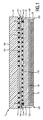
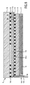
図1は、検出器モジュール1の第1の実施形態の断面図を示す。検出器モジュール1は、入射光子を電気信号に変換するための、例えばCZT及び/又はCdTe又は他の材料で作られた直接変換結晶10(以下、DiCOとも呼ばれる)を有する。直接変換結晶は、第1の表面に堆積されたカソードメタライゼーション100(カソード層とも呼ばれる)及び第2の表面に堆積されたアノードメタライゼーション101(アノード層とも呼ばれる)を有する。 FIG. 1 shows a cross-sectional view of a first embodiment of a detector module 1. The detector module 1 has a direct conversion crystal 10 (hereinafter also referred to as DiCO) made of, for example, CZT and / or CdTe or other material for converting incident photons into electrical signals. The direct conversion crystal has a cathode metallization 100 (also referred to as a cathode layer) deposited on a first surface and an anode metallization 101 (also referred to as an anode layer) deposited on a second surface.
検出器モジュール1は更に、直接変換結晶10と電気的に通信する集積回路12(例えばASIC)を有する。この実施形態において2つの集積回路12、12'が設けられており、それぞれの集積回路12、12'が、凹部120、120'を有するが、これは一般に必要ではない。集積回路は、直接変換結晶よりも小さい幅を有し、したがって一方の側面に幅方向の凹部120を形成する。
The detector module 1 further includes an integrated circuit 12 (eg, ASIC) in electrical communication with the
インタポーザ11は、直接変換結晶10と集積回路12、12'との間の電気的通信を提供するために、直接変換結晶10と集積回路12、12'との間に配置される。インタポーザ11は剛性素子あり、集積回路12、12'に面する直接変換結晶10のアノードメタライゼーション101と接触する個別の素子として形成される。この実施形態では、インタポーザ11は、はんだボール14によって直接変換結晶10のアノードメタライゼーション101にはんだ付けされる。インタポーザ11は更に、直接変換結晶10に面するASIC12、12'の表面に、はんだボール15によってはんだ付けされる。インタポーザ11が別個の素子として形成され扱われることができる限り、はんだ付け以外の接続を形成する他のやり方も可能である。例えば、熱圧着、室温接着、スタッドバンプ接合などを含む、任意の形態の接着、はんだ付け及び接合が使用されることができる。
The
好適には、剛性インタポーザ11は再配線機能を有し、RDLインタポーザとも呼ばれる。この目的のために、剛性インタポーザ11は、再配線接続16を有する。したがって、剛性インタポーザ11は、ASIC12、12'のピクセル接点を直接変換結晶10のピクセルに接続する。
Preferably, the
複数の出力経路を提供するマルチリードフレックスケーブル13、13'が提供される(この実施形態では、2つのフレックスケーブル13、13'が提供されるが、これは一般に必要ではない)。マルチリードフレックスケーブル13、13'はそれぞれ、直接変換結晶10に接続される第1の部分131、131'と、第1の部分131、131'に対し曲げられた第2の部分132、132'とを有する。第1の部分131、131'は、集積回路の幅に沿う方向であって、集積回路の長さに垂直な方向に配置される。第2の部分132、132'は、それぞれの凹部120、120'内に配置される。フレックスケーブル(例えばCuトラックを有する)13、13'は、例えばポリイミドで形成されることができ、したがって非常に小さい曲げ半径を有することができる。フレックスケーブル13、13'は、ASIC12、12'を外界に接続するASIC I/O/P(入力/出力/電力)パッドに接触する。
A
はんだボールを用いて接触させるためには、ボールサイズと融解温度の両方の階層(hierarchy、序列)が適用されることができる。温度の階層は、個々の異なるはんだ合金によって達成されることができる:フレックスケーブル13、13'はまず、温度T1で融解する合金15aではんだ付けされ、次に、インタポーザ11が、T2<T1で融解するはんだボール15により、ASIC12、12'のピクセルに接触され、最後のステップにおいて、低温で処理しなければならないDiCO結晶10が、T3<T2で融解するはんだボール14により、インタポーザ11の上側パッドに接触される。
To make contact using solder balls, both ball size and melting temperature hierarchy can be applied. The temperature hierarchy can be achieved by individual different solder alloys: the
任意には、図1に示すように、共通のヒートシンク17、例えばアルミニウムブロックが、インタポーザ11と反対側を向くASIC12、12'の表面121に配置される。ASIC12、12'とは反対側を向く表面側から、空気流18が冷却目的で供給されることができる。
Optionally, as shown in FIG. 1, a
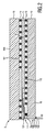
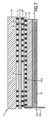
図2は、検出器モジュール2の第2の実施形態の断面図を示す。検出器モジュール1の第1の実施形態とは異なり、検出器モジュール2は単一のASIC12と単一のフレックスケーブル13とを有する。インタポーザ11の表面110にはキャビティ111が形成されている。キャビティ111内には、フレックスケーブル13の第1の部分131が配置される。キャビティ1は、インタポーザ11のコストを増大させうるが、インタポーザ11内のキャビティ111(又はミルドダウン領域)は、はんだボール15及び15aと同じボールサイズを使用するために必要なスペースを提供するので、検出器モジュール2のこの実施形態では、融解温度の階層のみが必要とされる。
FIG. 2 shows a cross-sectional view of a second embodiment of the detector module 2. Unlike the first embodiment of the detector module 1, the detector module 2 has a
検出器モジュール1、2の短いフレックスケーブル11、11'の場合、少数のはんだボール15aが、フレックスケーブル11、11'を曲げる曲げプロセスにおいて印加される力を受け入れなければならないので、機械的安定性が制限される。剛性RDLインタポーザ11は、例えばセラミック又はガラスで形成されることができる。
In the case of the
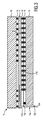
図3は、可撓材料で形成された1対1インタポーザ(すなわちRDL機能なし)を有する検出器モジュール3の第3の実施形態の断面図を示す。この1対1インタポーザ131aは、これにより、フレックスケーブル13aの第1の部分によって形成される。1対1インタポーザ131aの上には、剛性RDLインタポーザ11が、はんだボール19を使用するはんだ付けによって取り付けられる。
FIG. 3 shows a cross-sectional view of a third embodiment of a detector module 3 having a one-to-one interposer (ie without RDL function) formed of a flexible material. The one-to-one interposer 131a is thereby formed by the first portion of the flex cable 13a. On the one-to-one interposer 131a, the
フレックスケーブル13aは、I/O/P接点を検出器モジュール3の外界にもっていくという目的を果たす。RDLインタポーザ11の上には、DiCO材料10が、はんだボール14によってはんだ付けされる。この場合、非常に長いフレックスケーブル13aにより、可撓性部分の機械的安定性が最大にされる。欠点は、1対1インタポーザ131aの上下に2組のはんだボール15、19があることである。更にこの実施形態では、3つの異なる融解温度を有する融解温度階層が必要とされ得る。
The flex cable 13a serves the purpose of bringing the I / O / P contact to the outside of the detector module 3. On the
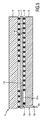
図4は、検出器モジュール4の第4の実施形態の断面図を示す。この実施形態では、可撓性インタポーザ131b(すなわち、フレックスケーブル13bの第1の部分)が、RDL機能をも実現し、すなわち、可撓性インタポーザ131bは、フレックスケーブルの第1の部分(1:1インタポーザ)及び剛性インタポーザの機能をあわせもつ。そのような検出器モジュール4は、それがセラミックで形成される場合、剛性RDLインタポーザを使用する検出器モジュールよりも優れたクロストーク低減を示すことさえできる。 FIG. 4 shows a cross-sectional view of a fourth embodiment of the detector module 4. In this embodiment, the flexible interposer 131b (ie, the first portion of the flex cable 13b) also implements the RDL function, ie, the flexible interposer 131b is the first portion of the flex cable (1: 1 interposer) and rigid interposer functions. Such a detector module 4 can even show a better crosstalk reduction when it is made of ceramic than a detector module using a rigid RDL interposer.
DiCO結晶10とフレックスインタポーザ131bとの間のはんだボール14の行による接続は、曲げ中に加えられる力に耐える必要があり、これは2つの点において重要である。はんだ接続が破損し、及び/又はやや脆いDiCO結晶10が曲げ中に損傷を受け、及び/又は結晶材料が、DiCO結晶ブロックから引きはがされることがありうる。更に、接続はんだボールのDiCO結晶端部に近接しているため、必要なモジュール間スペース(すなわち、隣接する検出器モジュール間のスペース)は、第1の実施形態よりもいくらか大きくなり得、第1の実施形態では、剛性インタポーザ11が、ASIC12上に延在し、インタポーザ11とDiCO結晶10との間のこの第1の行のはんだボール14を「保護」する。これは特に、第1の行のDiCO結晶アノードがDiCO結晶10の端部に非常に近い場合に当てはまる。DiCO結晶アノードは、一般に、相互接続用の面積よりもはるかに大きいので、第1の行のはんだマスクは、曲げのためのいくらかのスペースを獲得するためにDiCO結晶の内側に向けてシフトされることができる。すなわち、アノードのピッチは維持されるが、第1の行のはんだボール14は、意図的にシフトされ、その結果、次の行までのピッチがわずかに小さくなる。
The connection by the row of
図5は、検出器モジュール5の第5の実施形態の断面図を示す。この実施形態では、後者の問題が、1対1フレックスケーブル13c、具体的にはその第1の部分131cを、剛性RDLインタポーザ11に接合することによって、一層洗練された態様で解決される。そのような接合を得るために多数の方法が存在し、それらには以下が含まれる。
・結果的に得られる直列抵抗が低く保たれる限り(例えば、10オームより小さい)、両方の基板をACF(異方性導電接着剤)で接着する。
・熱圧着。
・常温接合(商業サプライヤによって提供される);この接合プロセスでは、レーザが、2つの部分の互いに接触する表面を局所的に加熱し、その結果、プラズマ層をもたらし、それにより接合を形成する。このプロセスは、基板を接合するだけでなく、電気的接続も形成する("No-Compromise multi-material solutions with ATB ambient temperature bonding". Richard Bijlard, CMN Vol. 8 No. 7を参照)。
FIG. 5 shows a cross-sectional view of a fifth embodiment of the detector module 5. In this embodiment, the latter problem is solved in a more sophisticated manner by joining the one-to-
Bond both substrates with ACF (anisotropic conductive adhesive) as long as the resulting series resistance is kept low (eg, less than 10 ohms).
-Thermocompression bonding.
Room temperature bonding (provided by a commercial supplier); in this bonding process, the laser locally heats the two contacting surfaces of the two parts, resulting in a plasma layer, thereby forming the bond. This process not only bonds the substrates, but also makes electrical connections (see "No-Compromise multi-material solutions with ATB ambient temperature bonding". Richard Bijlard, CMN Vol. 8 No. 7).
剛性RDLインタポーザ11は、第1の行のはんだボール14を良好に保護する。剛性RDLインタポーザ11が、上述したトラックの許容密度の制限を伴ってセラミックで製造される場合、欠点は、剛性RDLインタポーザ11のより大きなクロストーク容量であり得る;フレックス1対1インタポーザ13cに結合されるガラス製のRDLインタポーザの組み合わせは、より低いクロスカップリングキャパシタンスを提供し、したがって、これは、DiCO結晶10が曲げ中の力に対し良好に保護されるとともに、DiCO結晶10からはんだボールを引き離すことが、インタポーザ11によって防止されるので、良い解決策である。
The
図6は、反対の組み合わせ、すなわち剛性の1対1インタポーザ11aに低温接合されるフレックスRDLインタポーザ131dを利用する検出器モジュール6の第6の実施形態の断面図を示す。これは、フレックスインタポーザのクロストークキャパシタンスの減少に関して利益を提供し、脆いDiCO結晶10に曲げによるダメージを与えるリスクを排除する。曲げの間に、はんだボール14の第1の行14aに及ぼされる力が、1:1インタポーザ11a(セラミック又はガラス製)とフレックスケーブル13dとの間の接合接続に損傷を与えるという問題がありうる。1対1インタポーザ11aの第1の行14のところにのみ小さなRDL機能を導入することによって、この問題は大幅に軽減されることができる。この選択肢では、セラミック製の1対1インタポーザ11aが、フレックスケーブル13dと組み合わされて使用されることができる;ガラスは、その機械的特性のために回転ガントリ上では十分に信頼できないことがありうる。
FIG. 6 shows a cross-sectional view of a sixth embodiment of a detector module 6 that utilizes a flex RDL interposer 131d that is cold bonded to the opposite combination, a rigid one-to-
図7は、検出器モジュール7の第7の実施形態の断面図を示す。この実施形態では、フレックスインタポーザ131dが、はんだボール20の行によって剛性インタポーザ11aに接触される。
FIG. 7 shows a cross-sectional view of a seventh embodiment of the detector module 7. In this embodiment, the flex interposer 131d is brought into contact with the
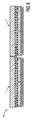
図8は、第1の実施形態1による(あるいは任意の他の実施形態に従う)2つの検出器モジュール1、1'を有する検出器50の実施形態の断面図を示す。図8に示されるように、検出器モジュール1、1'は、それらの間に空いたスペースがほとんどない状態で、互いに非常に接近して互いに隣接して配置され得る。
FIG. 8 shows a cross-sectional view of an embodiment of a
本発明が、図面及び前述の説明において詳しく図示され説明されたが、そのような図示及び説明は、例示的又は説明的であり、限定的なものではないと考えられるべきである。本発明は、開示された実施形態に限定されない。開示される実施形態に対する他の変更は、図面、開示、及び添付の特許請求の範囲の検討から、請求項に記載の発明を実施する際に当業者によって理解され、達成されることができる。 While the invention has been illustrated and described in detail in the drawings and foregoing description, such illustration and description are to be considered illustrative or exemplary and not restrictive. The invention is not limited to the disclosed embodiments. Other modifications to the disclosed embodiments can be understood and attained by those skilled in the art in practicing the claimed invention, from a study of the drawings, the disclosure, and the appended claims.
特許請求の範囲において、「含む、有する(comprising)」という語は、他の構成要素又はステップを除外するものではなく、不定冠詞「a」又は「an」は複数性を除外しない。単一の構成要素又は他のユニットが特許請求の範囲に記載のいくつかのアイテムの機能を果たすことができる。特定の手段が互いに異なる従属請求項に記載されているという単なる事実は、これらの手段の組み合わせが有利に使用されることができないことを示すものではない。 In the claims, the word “comprising” does not exclude other elements or steps, and the indefinite article “a” or “an” does not exclude a plurality. A single component or other unit may fulfill the functions of several items recited in the claims. The mere fact that certain measures are recited in mutually different dependent claims does not indicate that a combination of these measured cannot be used to advantage.
請求項中の如何なる参照符号も本発明の範囲を限定するものとして解釈されるべきでない。 Any reference signs in the claims should not be construed as limiting the scope of the invention.
Claims (13)
前記直接変換結晶と電気的に通信する集積回路であって、前記集積回路は、前記直接変換結晶の幅よりも小さい幅を有し、それにより前記集積回路の側面に、幅方向の凹部を形成する、集積回路と、
前記直接変換結晶と前記集積回路との間に配され、前記直接変換結晶と前記集積回路との間の電気通信を提供するインタポーザであって、前記インタポーザは、前記集積回路に面する前記直接変換結晶のアノードメタライゼーションと接着され、はんだ付けされ、又は接合される別個の要素として形成される、インタポーザと、
複数の出力経路を提供するマルチリードフレックスケーブルであって、一方の面が前記直接変換結晶に接続され、他方の面が前記集積回路に接続された第1の部分及び前記第1の部分に対し曲げられ前記凹部内に配された第2の部分を有する、マルチリードフレックスケーブルと、
を有する検出器モジュール。 A direct conversion crystal for converting incident photons into an electrical signal having a cathode metallization deposited on a first surface and an anode metallization deposited on a second surface;
An integrated circuit in electrical communication with the direct conversion crystal, the integrated circuit having a width smaller than the width of the direct conversion crystal, thereby forming a widthwise recess in a side surface of the integrated circuit An integrated circuit,
An interposer disposed between the direct conversion crystal and the integrated circuit and providing electrical communication between the direct conversion crystal and the integrated circuit, the interposer facing the integrated circuit An interposer formed as a separate element that is glued, soldered or joined to the crystalline anode metallization;
A multi-lead flex cable providing a plurality of output paths, wherein the first surface is connected to the direct conversion crystal and the other surface is connected to the integrated circuit with respect to the first portion and the first portion. A multi-lead flex cable having a second portion bent and disposed in the recess;
Having a detector module.
インタポーザを個別の素子として形成するステップと、
入射光子を電気信号に変換する直接変換結晶のアノードメタライゼーションに前記インタポーザを、接着、はんだ付け又は接合によって接触させるステップであって、前記直接変換結晶は、その第1の表面上に堆積されたカソードメタライゼーション及び第2の表面上に堆積されたアノードメタライゼーションを有する、ステップと、
前記インタポーザの、前記直接変換結晶と反対側の面に集積回路を配するステップであって、前記インタポーザは、前記集積回路と前記直接変換結晶との間の電気通信を提供し、前記集積回路は、前記直接変換結晶の幅より小さい幅を有し、それにより前記集積回路の側面に幅方向の凹部を形成する、ステップと、
複数の出力経路を提供するマルチリードフレックスケーブルを前記凹部内に配するステップであって、前記マルチリードフレックスケーブルの第1の部分は、一方の面が前記直接変換結晶に接続され、他方の面が前記集積回路の対向する表面に接続され、前記第1の部分に対し曲げられる第2の部分が、前記凹部内に配される、ステップと、
を有する方法。 A method of manufacturing a detector module according to claim 1, comprising:
Forming the interposer as individual elements;
Contacting the interposer by adhesion, soldering or bonding to an anode metallization of a direct conversion crystal that converts incident photons into an electrical signal, the direct conversion crystal being deposited on its first surface Having a cathode metallization and an anode metallization deposited on the second surface;
Disposing an integrated circuit on a surface of the interposer opposite the direct conversion crystal, the interposer providing electrical communication between the integrated circuit and the direct conversion crystal, the integrated circuit comprising: Having a width smaller than the width of the direct conversion crystal, thereby forming a widthwise recess on a side surface of the integrated circuit; and
Placing a multi-lead flex cable providing a plurality of output paths into the recess, wherein the first portion of the multi-lead flex cable has one side connected to the direct conversion crystal and the other side A second portion that is connected to an opposing surface of the integrated circuit and that is bent relative to the first portion is disposed in the recess;
Having a method.
Applications Claiming Priority (3)
| Application Number | Priority Date | Filing Date | Title |
|---|---|---|---|
| EP16179411 | 2016-07-14 | ||
| EP16179411.0 | 2016-07-14 | ||
| PCT/EP2017/067852 WO2018011399A1 (en) | 2016-07-14 | 2017-07-14 | Detector module, detector, imaging apparatus and method of manufacturing a detector module |
Publications (2)
| Publication Number | Publication Date |
|---|---|
| JP2019523402A true JP2019523402A (en) | 2019-08-22 |
| JP6842528B2 JP6842528B2 (en) | 2021-03-17 |
Family
ID=56740808
Family Applications (1)
| Application Number | Title | Priority Date | Filing Date |
|---|---|---|---|
| JP2019500891A Active JP6842528B2 (en) | 2016-07-14 | 2017-07-14 | Manufacture method of detector module, detector, imaging device and detector module |
Country Status (7)
| Country | Link |
|---|---|
| US (1) | US10868074B2 (en) |
| EP (1) | EP3485514B1 (en) |
| JP (1) | JP6842528B2 (en) |
| CN (1) | CN109478556B (en) |
| BR (1) | BR112019000429A2 (en) |
| RU (1) | RU2019103999A (en) |
| WO (1) | WO2018011399A1 (en) |
Cited By (2)
| Publication number | Priority date | Publication date | Assignee | Title |
|---|---|---|---|---|
| JP2023534365A (en) * | 2020-05-13 | 2023-08-09 | デクトリス アクチェンゲゼルシャフト | radiation detector |
| US12468053B2 (en) | 2023-03-07 | 2025-11-11 | Canon Kabushiki Kaisha | Radiation detection apparatus |
Families Citing this family (3)
| Publication number | Priority date | Publication date | Assignee | Title |
|---|---|---|---|---|
| CN111640131B (en) * | 2020-05-29 | 2021-05-18 | 广东利元亨智能装备股份有限公司 | Cell coating detection method, device and electronic equipment |
| WO2022122374A2 (en) | 2020-12-10 | 2022-06-16 | Ams-Osram Ag | X-ray radiation sensor device |
| US20240219589A1 (en) * | 2022-01-31 | 2024-07-04 | Redlen Technologies, Inc. | Direct attach radiation detector structures including a carrier board and methods of fabrication thereof |
Citations (4)
| Publication number | Priority date | Publication date | Assignee | Title |
|---|---|---|---|---|
| JP2006026401A (en) * | 2004-06-29 | 2006-02-02 | General Electric Co <Ge> | Radiation imaging system detector |
| JP2009078143A (en) * | 2007-09-26 | 2009-04-16 | General Electric Co <Ge> | Method and apparatus for freely collecting energy identification data |
| US20100327173A1 (en) * | 2009-06-29 | 2010-12-30 | Charles Gerard Woychik | Integrated Direct Conversion Detector Module |
| WO2016066850A1 (en) * | 2014-10-31 | 2016-05-06 | Koninklijke Philips N.V. | Sensor device and imaging system for detecting radiation signals |
Family Cites Families (10)
| Publication number | Priority date | Publication date | Assignee | Title |
|---|---|---|---|---|
| JP2002158341A (en) | 2000-11-17 | 2002-05-31 | Canon Inc | Imaging device |
| US7564125B2 (en) * | 2002-12-06 | 2009-07-21 | General Electric Company | Electronic array and methods for fabricating same |
| DE102005037902A1 (en) | 2005-08-10 | 2007-02-15 | Siemens Ag | Detector module, detector and computed tomography device |
| JP4046138B2 (en) * | 2006-05-24 | 2008-02-13 | 株式会社村田製作所 | Work transfer device and electronic component transfer device |
| JP5281484B2 (en) * | 2009-05-28 | 2013-09-04 | 浜松ホトニクス株式会社 | Radiation detection unit |
| JP5358509B2 (en) * | 2010-04-15 | 2013-12-04 | 浜松ホトニクス株式会社 | Radiation detector module |
| US20130049151A1 (en) * | 2011-08-31 | 2013-02-28 | General Electric Company | Anode-illuminated radiation detector |
| FI124818B (en) | 2011-10-06 | 2015-02-13 | Advacam Oy | Hybrid pixel detector construction and a method for its manufacture |
| WO2013176657A1 (en) | 2012-05-22 | 2013-11-28 | Analogic Corporaton | Detection system and detector array interconnect assemblies |
| JP5424371B1 (en) * | 2013-05-08 | 2014-02-26 | 誠 雫石 | Solid-state imaging device and imaging apparatus |
-
2017
- 2017-07-14 WO PCT/EP2017/067852 patent/WO2018011399A1/en not_active Ceased
- 2017-07-14 RU RU2019103999A patent/RU2019103999A/en not_active Application Discontinuation
- 2017-07-14 EP EP17737300.8A patent/EP3485514B1/en active Active
- 2017-07-14 BR BR112019000429A patent/BR112019000429A2/en not_active Application Discontinuation
- 2017-07-14 US US16/316,051 patent/US10868074B2/en active Active
- 2017-07-14 JP JP2019500891A patent/JP6842528B2/en active Active
- 2017-07-14 CN CN201780043549.0A patent/CN109478556B/en active Active
Patent Citations (5)
| Publication number | Priority date | Publication date | Assignee | Title |
|---|---|---|---|---|
| JP2006026401A (en) * | 2004-06-29 | 2006-02-02 | General Electric Co <Ge> | Radiation imaging system detector |
| JP2009078143A (en) * | 2007-09-26 | 2009-04-16 | General Electric Co <Ge> | Method and apparatus for freely collecting energy identification data |
| US20100327173A1 (en) * | 2009-06-29 | 2010-12-30 | Charles Gerard Woychik | Integrated Direct Conversion Detector Module |
| JP2011007789A (en) * | 2009-06-29 | 2011-01-13 | General Electric Co <Ge> | Integrated direct conversion detector module |
| WO2016066850A1 (en) * | 2014-10-31 | 2016-05-06 | Koninklijke Philips N.V. | Sensor device and imaging system for detecting radiation signals |
Cited By (3)
| Publication number | Priority date | Publication date | Assignee | Title |
|---|---|---|---|---|
| JP2023534365A (en) * | 2020-05-13 | 2023-08-09 | デクトリス アクチェンゲゼルシャフト | radiation detector |
| JP7626784B2 (en) | 2020-05-13 | 2025-02-04 | デクトリス アクチェンゲゼルシャフト | Radiation detector |
| US12468053B2 (en) | 2023-03-07 | 2025-11-11 | Canon Kabushiki Kaisha | Radiation detection apparatus |
Also Published As
| Publication number | Publication date |
|---|---|
| US20190280036A1 (en) | 2019-09-12 |
| US10868074B2 (en) | 2020-12-15 |
| JP6842528B2 (en) | 2021-03-17 |
| EP3485514A1 (en) | 2019-05-22 |
| WO2018011399A1 (en) | 2018-01-18 |
| BR112019000429A2 (en) | 2019-04-30 |
| CN109478556A (en) | 2019-03-15 |
| EP3485514B1 (en) | 2020-09-09 |
| RU2019103999A (en) | 2020-08-14 |
| CN109478556B (en) | 2023-07-14 |
Similar Documents
| Publication | Publication Date | Title |
|---|---|---|
| JP6842528B2 (en) | Manufacture method of detector module, detector, imaging device and detector module | |
| CN101199434B (en) | Modular sensor assembly and methods of fabricating the same | |
| TWI328867B (en) | Integrated structure and method for fabricating the same | |
| US8975583B2 (en) | 3D stacked uncooled IR sensor device and method | |
| WO2003077318A1 (en) | Sensor | |
| CN102651357B (en) | Semiconductor device, sensor and electronic equipment | |
| JP6021618B2 (en) | Imaging apparatus, endoscope, and manufacturing method of imaging apparatus | |
| US20100327173A1 (en) | Integrated Direct Conversion Detector Module | |
| CN104135933A (en) | Compact sensor module | |
| JP2010199148A (en) | Semiconductor sensor device and method of manufacturing thereof, package and method of manufacturing thereof, module and method of manufacturing thereof, and electronic device | |
| US11682745B2 (en) | Photon detector array assembly | |
| US10334143B2 (en) | Image pickup apparatus having wiring board with alternately arranged flying leads | |
| WO2004064162A1 (en) | Wiring substrate and radiation detector using same | |
| JP7444850B2 (en) | Semiconductor device, imaging device, and semiconductor device manufacturing method | |
| JPWO2017122449A1 (en) | Semiconductor device and imaging device | |
| CN103296036A (en) | X-ray detector and manufacturing method thereof | |
| JPWO2020105432A1 (en) | Stacked semiconductor device and multiple chips used for it | |
| US20240145521A1 (en) | Radiation imaging device | |
| CN105810705A (en) | Package structure of high-pixel image sensing chip and fabrication method of package structure | |
| US12557404B2 (en) | Module assembly for detection of X-ray radiation | |
| JP2009147212A (en) | Photodetector and photodetection device using photodetector | |
| TWI801748B (en) | Sensor arrangement and method for fabricating a sensor arrangement | |
| JP4799746B2 (en) | Radiation detector module | |
| JP2002261262A (en) | Image sensor and method of manufacturing the same | |
| Tick et al. | TSV processing of Medipix3 wafers by CEA-LETI: a progress report |
Legal Events
| Date | Code | Title | Description |
|---|---|---|---|
| A621 | Written request for application examination |
Free format text: JAPANESE INTERMEDIATE CODE: A621 Effective date: 20200115 |
|
| A871 | Explanation of circumstances concerning accelerated examination |
Free format text: JAPANESE INTERMEDIATE CODE: A871 Effective date: 20200115 |
|
| A975 | Report on accelerated examination |
Free format text: JAPANESE INTERMEDIATE CODE: A971005 Effective date: 20200122 |
|
| A977 | Report on retrieval |
Free format text: JAPANESE INTERMEDIATE CODE: A971007 Effective date: 20200424 |
|
| A131 | Notification of reasons for refusal |
Free format text: JAPANESE INTERMEDIATE CODE: A131 Effective date: 20200602 |
|
| A521 | Request for written amendment filed |
Free format text: JAPANESE INTERMEDIATE CODE: A523 Effective date: 20200902 |
|
| A131 | Notification of reasons for refusal |
Free format text: JAPANESE INTERMEDIATE CODE: A131 Effective date: 20200924 |
|
| A521 | Request for written amendment filed |
Free format text: JAPANESE INTERMEDIATE CODE: A523 Effective date: 20201221 |
|
| TRDD | Decision of grant or rejection written | ||
| A01 | Written decision to grant a patent or to grant a registration (utility model) |
Free format text: JAPANESE INTERMEDIATE CODE: A01 Effective date: 20210126 |
|
| A61 | First payment of annual fees (during grant procedure) |
Free format text: JAPANESE INTERMEDIATE CODE: A61 Effective date: 20210219 |
|
| R150 | Certificate of patent or registration of utility model |
Ref document number: 6842528 Country of ref document: JP Free format text: JAPANESE INTERMEDIATE CODE: R150 |
|
| R250 | Receipt of annual fees |
Free format text: JAPANESE INTERMEDIATE CODE: R250 |
|
| R250 | Receipt of annual fees |
Free format text: JAPANESE INTERMEDIATE CODE: R250 |
|
| R250 | Receipt of annual fees |
Free format text: JAPANESE INTERMEDIATE CODE: R250 |