JP2020003629A - Optical scanner - Google Patents
Optical scanner Download PDFInfo
- Publication number
- JP2020003629A JP2020003629A JP2018122611A JP2018122611A JP2020003629A JP 2020003629 A JP2020003629 A JP 2020003629A JP 2018122611 A JP2018122611 A JP 2018122611A JP 2018122611 A JP2018122611 A JP 2018122611A JP 2020003629 A JP2020003629 A JP 2020003629A
- Authority
- JP
- Japan
- Prior art keywords
- rotation axis
- reflection plate
- magnetic element
- light
- magnetic
- Prior art date
- Legal status (The legal status is an assumption and is not a legal conclusion. Google has not performed a legal analysis and makes no representation as to the accuracy of the status listed.)
- Pending
Links
Images






Landscapes
- Mechanical Optical Scanning Systems (AREA)
- Mechanical Light Control Or Optical Switches (AREA)
- Optical Radar Systems And Details Thereof (AREA)
- Measurement Of Optical Distance (AREA)
Abstract
【課題】設置スペースを抑えて広い走査対象領域を走査することができる光走査装置を提供する。【解決手段】光走査装置1が、第1光源101と、第2光源102と、両面のうちの一方に第1光源101からの照射光を反射する第1反射面111が形成され、他方に第2光源102からの照射光を反射する第2反射面112が形成された反射板110と、反射板110の面方向に延在する第1回動軸121を中心に反射板110を回動可能に支持する第1支持部120と、第1回動軸121を中心に反射板110を回動させる駆動部130と、を備えることを特徴とする。【選択図】図1PROBLEM TO BE SOLVED: To provide an optical scanning device capable of scanning a wide scanning target area while suppressing an installation space. SOLUTION: The optical scanning device 1 has a first light source 101, a second light source 102, and a first reflecting surface 111 for reflecting the irradiation light from the first light source 101 on one of both surfaces thereof. The reflector 110 is rotated around a reflector 110 formed with a second reflecting surface 112 that reflects the irradiation light from the second light source 102 and a first rotating shaft 121 extending in the plane direction of the reflector 110. It is characterized by including a first support portion 120 that can support the light source 120, and a drive portion 130 that rotates the reflector 110 around the first rotation shaft 121. [Selection diagram] Fig. 1
Description
本発明は、光源からの照射光で走査対象領域を走査する光走査装置に関する。 The present invention relates to an optical scanning device that scans an area to be scanned with irradiation light from a light source.
従来、光源からの照射光で走査対象領域を走査し、その走査対象領域からの戻り光が光ディテクタで検出されるまでの時間に基づいて、走査対象領域に存在する物体までの距離等を測定する光走査装置が知られている(例えば、特許文献1参照。)。特許文献1に記載の光走査装置では、光源からの照射光が反射板で反射されて走査対象領域へと照射される。反射板の回動によって照射光の反射方向が変わり、これにより走査が行われる。走査対象領域からの戻り光は、反射板で反射されて光ディテクタへと向かう。
Conventionally, the scanning target area is scanned with the irradiation light from the light source, and the distance to the object existing in the scanning target area is measured based on the time until the return light from the scanning target area is detected by the light detector. A known optical scanning device is known (for example, see Patent Document 1). In the optical scanning device described in
ここで、上記の光走査装置によってなるべく広い走査対象領域を走査したいとの要望がある。このような要望に応えるために、光走査装置を複数台並べて配置することが考えられる。このとき、上記の光走査装置では、反射板の回動が、磁気回路を用いて行われている。このため、光走査装置を複数台並べて配置するに当たっては、磁気回路どうしの磁気的な干渉を回避するために、ある程度の間隔を開けて光走査装置を配置する必要がある。その結果、このように複数台の光走査装置を用いて広い走査対象領域を走査する構成では、設置に相当な広さの設置スペースが必要となる。 Here, there is a demand for scanning the scanning target area as large as possible by the optical scanning device. In order to meet such a demand, it is conceivable to arrange a plurality of optical scanning devices side by side. At this time, in the above-described optical scanning device, the rotation of the reflection plate is performed using a magnetic circuit. For this reason, when arranging a plurality of optical scanning devices side by side, it is necessary to arrange the optical scanning devices at a certain interval in order to avoid magnetic interference between magnetic circuits. As a result, in such a configuration in which a wide scanning target area is scanned using a plurality of optical scanning devices, a considerably large installation space is required for installation.
したがって、本発明の課題は、設置スペースを抑えて広い走査対象領域を走査することができる光走査装置を提供すること等が一例として挙げられる。 Therefore, an object of the present invention is to provide, for example, an optical scanning device capable of scanning a wide scanning target area with a small installation space.
前述した課題を解決し目的を達成するために、請求項1に記載の本発明の光走査装置は、第1光源と、第2光源と、両面のうちの一方に前記第1光源からの照射光を反射する第1反射面が形成され、他方に前記第2光源からの照射光を反射する第2反射面が形成された反射板と、前記反射板の面方向に延在する第1回動軸を中心に前記反射板を回動可能に支持する第1支持部と、前記第1回動軸を中心に前記反射板を回動させる駆動部と、を備えることを特徴とする。
In order to solve the above-described problem and achieve the object, an optical scanning device according to the present invention according to
以下、本発明の実施形態を説明する。本発明の実施形態に係る光走査装置は、第1光源と、第2光源と、反射板と、第1支持部と、駆動部と、を備える。反射板は、両面のうちの一方に第1光源からの照射光を反射する第1反射面が形成され、他方に第2光源からの照射光を反射する第2反射面が形成されている。第1支持部は、反射板の面方向に延在する第1回動軸を中心に反射板を回動可能に支持する。そして、駆動部は、第1回動軸を中心に反射板を回動させる。 Hereinafter, embodiments of the present invention will be described. An optical scanning device according to an embodiment of the present invention includes a first light source, a second light source, a reflector, a first support, and a driver. The reflection plate has a first reflection surface that reflects irradiation light from the first light source on one of both surfaces, and a second reflection surface that reflects irradiation light from the second light source on the other. The first supporter supports the reflector so as to be rotatable about a first rotation axis extending in a plane direction of the reflector. Then, the drive unit rotates the reflection plate about the first rotation axis.
本実施形態の光走査装置によれば、両面反射タイプの反射板における各反射面で反射された各光源からの照射光が、反射板が回動したときに各反射面での反射範囲に応じた走査対象領域を走査することとなる。これにより、2つの走査対象領域を足し合わせた広い走査対象領域を走査することができる。そして、このような広い走査対象領域が、両面反射タイプの1枚の反射板を用いた1台の光走査装置で実現されていることから、設置スペースを抑えることができる。 According to the optical scanning device of the present embodiment, the irradiation light from each light source reflected on each reflection surface of the double-sided reflection type reflection plate depends on the reflection range on each reflection surface when the reflection plate rotates. The scanning target area is scanned. Thus, it is possible to scan a wide scanning target area obtained by adding the two scanning target areas. Since such a wide scanning target area is realized by one optical scanning device using one reflection plate of a double-sided reflection type, the installation space can be reduced.
ここで、本実施形態の光走査装置では、駆動部は、反射板の第1回動軸とずれた位置に取付けられる第1磁気素子、及び、この第1磁気素子に対して磁気を加えて、第1回動軸を中心に反射板を回動させる第1磁気アクチュエータ、を有している。これにより、第1磁気アクチュエータで第1磁気素子を磁気駆動するという簡単な構造で反射板を確実に回動させることができるので好適である。 Here, in the optical scanning device of the present embodiment, the drive unit applies a magnetism to the first magnetic element mounted at a position shifted from the first rotation axis of the reflection plate, and applies a magnetism to the first magnetic element. And a first magnetic actuator for rotating the reflection plate about the first rotation axis. This is preferable because the reflector can be reliably rotated with a simple structure in which the first magnetic element is magnetically driven by the first magnetic actuator.
また、本実施形態の光走査装置では、第1回動軸が、反射板を、第1回動軸に対する直交方向について長さが異なる2つの領域に二分し、第1磁気素子が、長さが短い方の領域に取り付けられている。 Further, in the optical scanning device of the present embodiment, the first rotation axis bisects the reflection plate into two regions having different lengths in the direction orthogonal to the first rotation axis, and the first magnetic element has the length. Are attached to the shorter area.
これにより、2つの領域のうちの長い方の領域について、第1磁気素子の駆動量に対して、第1回動軸を中心とした大きな回動量を得ることができる。照射光や戻り光は、第1磁気素子を避けて、この長い方の領域で反射されることとなるので、第1磁気素子の駆動量に対して大きな走査量を得ることができるので、一層広い走査対象領域を走査することができる。 Accordingly, a larger rotation amount about the first rotation axis can be obtained with respect to the driving amount of the first magnetic element in the longer one of the two regions. Irradiation light and return light are reflected by this longer area, avoiding the first magnetic element, and a large scanning amount can be obtained with respect to the driving amount of the first magnetic element. A wide scanning target area can be scanned.
また、本実施形態の光走査装置は、反射板との間に間隙を開けるとともに、第1光源からの照射光及び第2光源からの照射光それぞれが反射された反射光の出射側を除いて反射板を囲むように面内方向に延在するフレームを更に備えている。そして、第1支持部は、反射板とフレームとの間の間隙に設けられている。 In addition, the optical scanning device of the present embodiment has a gap between the light source and the reflection plate, and excludes the emission side of the reflected light from which the irradiation light from the first light source and the irradiation light from the second light source are reflected. The frame further includes a frame extending in an in-plane direction so as to surround the reflection plate. The first support is provided in a gap between the reflector and the frame.
これにより、反射板を所定の取付け箇所に、上記のフレームを利用することで容易に取り付けることができる。そして、そのフレームが、上記の反射光の出射側を除いて反射板を囲むように面内方向に延在することから、その反射光や、走査対象領域からの戻り光を、フレームが遮ることで走査可能な領域を狭めてしまうといった事態を回避することができる。 Thus, the reflector can be easily attached to a predetermined attachment location by using the above-described frame. Then, since the frame extends in the in-plane direction so as to surround the reflector except for the emission side of the reflected light, the frame blocks the reflected light and the return light from the scanning target area. It is possible to avoid a situation in which the scannable area is narrowed by using.
また、本実施形態の光走査装置は、第1回動軸とは異なる方向に延在する第2回動軸を中心に反射板を回動可能に支持する第2支持部を備えている。そして、駆動部は、第2磁気素子及び第2磁気アクチュエータを有している。第2磁気素子は、反射板において、第1回動軸に対して第1磁気素子と同じ側にずれた位置に、当該第1磁気素子との間に第2回動軸を挟んで取り付けられる。また、第2磁気アクチュエータは、第2磁気素子に磁気を加え、第1磁気アクチュエータと協働して第1回動軸及び第2回動軸それぞれを中心に反射板を回動させる。 In addition, the optical scanning device of the present embodiment includes a second support unit that supports the reflection plate so as to be rotatable around a second rotation axis extending in a direction different from the first rotation axis. The drive section has a second magnetic element and a second magnetic actuator. The second magnetic element is attached to the reflector at a position shifted to the same side as the first magnetic element with respect to the first rotation axis with the second rotation axis interposed between the second magnetic element and the first magnetic element. . The second magnetic actuator applies magnetism to the second magnetic element, and cooperates with the first magnetic actuator to rotate the reflector about the first rotation axis and the second rotation axis.
これにより、反射板を、第1回動軸と第2回動軸との二軸で回動させることができる。つまり、走査対象領域を二次元的に走査可能な光走査装置を構築することができる。 Thereby, the reflection plate can be rotated about two axes of the first rotation axis and the second rotation axis. That is, an optical scanning device capable of two-dimensionally scanning the scanning target area can be constructed.
また、本実施形態の光走査装置は、以下の構成を有するものであってもよい。即ち、第1支持部が、その延在方向について伸縮可能な伸縮構造を有することで、第1回動軸とは異なる方向に延在する第2回動軸を中心とした回動についても可能に反射板を支持するものであってもよい。この場合にも、駆動部は、第2磁気素子及び第2磁気アクチュエータを有している。第2磁気素子は、反射板において、第1回動軸に対して第1磁気素子と同じ側にずれた位置に、当該第1磁気素子との間に第2回動軸を挟んで取り付けられる。第2磁気アクチュエータは、第2磁気素子に磁気を加え、第1磁気アクチュエータと協働して第1回動軸及び第2回動軸それぞれを中心に反射板を回動させる。 Further, the optical scanning device of the present embodiment may have the following configuration. That is, since the first support portion has a telescopic structure that can expand and contract in the direction in which the first support portion extends, the first support portion can be rotated around a second rotation shaft that extends in a direction different from the first rotation shaft. May support the reflector. Also in this case, the drive unit has the second magnetic element and the second magnetic actuator. The second magnetic element is attached to the reflector at a position shifted to the same side as the first magnetic element with respect to the first rotation axis with the second rotation axis interposed between the second magnetic element and the first magnetic element. . The second magnetic actuator applies magnetism to the second magnetic element, and cooperates with the first magnetic actuator to rotate the reflector about the first rotation axis and the second rotation axis.
このような構成によっても、反射板を、第1回動軸と第2回動軸との二軸で回動させることができる。つまり、走査対象領域を二次元的に走査可能な光走査装置を構築することができる。 Even with such a configuration, the reflection plate can be rotated about two axes of the first rotation axis and the second rotation axis. That is, an optical scanning device capable of two-dimensionally scanning the scanning target area can be constructed.
また、反射板を二軸で回動させる本実施形態の光走査装置では、第1回動軸が、反射板を、第1回動軸に対する直交方向について長さが異なる2つの領域に二分し、第2回動軸が、反射板を、第2回動軸に対する直交方向について二等分する。そして、第1磁気素子及び第2磁気素子は、長さが短い方の領域が第2回動軸で二等分された2つの領域部分に、それぞれ取り付けられている。 Further, in the optical scanning device according to the present embodiment in which the reflection plate is rotated about two axes, the first rotation axis bisects the reflection plate into two regions having different lengths in a direction orthogonal to the first rotation axis. , The second rotation axis bisects the reflection plate in a direction orthogonal to the second rotation axis. Then, the first magnetic element and the second magnetic element are respectively attached to two area portions in which the shorter area is bisected by the second rotation axis.
これにより、第1回動軸を中心とした反射板の回動によって一層広い走査対象領域を走査することができ、反射板を二等分する第2回動軸を中心とした反射板の回動によってバランスよく走査することができる。 Thus, a wider scanning target area can be scanned by the rotation of the reflector about the first rotation axis, and the rotation of the reflector about the second rotation axis that bisects the reflector can be performed. Scanning can be performed in good balance by movement.
また、本実施形態の光走査装置は、第1受光素子、第2受光素子、第1光学素子、及び第2光学素子を備えている。第1受光素子は、光を検出する素子であり、第2受光素子は、その光とは異なる光路の光を検出する素子である。第1光学素子は、第1光源からの照射光で第1走査対象領域が走査された結果、当該第1走査対象領域から戻って第1反射面で反射された戻り光を第1受光素子に導光する素子である。また、第2光学素子は、第2光源からの照射光で第2走査対象領域が走査された結果、当該第2走査対象領域から戻って第2反射面で反射された戻り光を第2受光素子に導光する素子である。 Further, the optical scanning device according to the present embodiment includes a first light receiving element, a second light receiving element, a first optical element, and a second optical element. The first light receiving element is an element that detects light, and the second light receiving element is an element that detects light in an optical path different from the light. The first optical element scans the first scan target area with the irradiation light from the first light source, and returns the return light from the first scan target area and reflected by the first reflection surface to the first light receiving element. It is a light guiding element. Further, the second optical element receives the return light returned from the second scanning target area and reflected by the second reflecting surface as a result of the second scanning target area being scanned with the irradiation light from the second light source, and receiving the second light. An element that guides light to the element.
これにより、第1走査対象領域及び第2走査対象領域それぞれについての走査結果を、第1受光素子及び第2受光素子での検出結果という数値データとして取得し、様々な処理装置での利用に供することができる。 As a result, the scanning results for each of the first scanning target area and the second scanning target area are acquired as numerical data of the detection results of the first light receiving element and the second light receiving element, and are used in various processing devices. be able to.
以下、本発明の実施例について図を参照して具体的に説明する。まず、第1実施例について説明する。 Hereinafter, embodiments of the present invention will be specifically described with reference to the drawings. First, a first embodiment will be described.
図1は、本発明の第1実施例に係る光走査装置を示す模式図である。 FIG. 1 is a schematic diagram showing an optical scanning device according to a first embodiment of the present invention.
図1に示されている光走査装置1は、第1光源101、第2光源102、第1受光素子103、第2受光素子104、第1光学素子105、第2光学素子106、反射板110、第1支持部120、及び駆動部130、を備える。
The
この光走査装置1は、第1光源101からの照射光L11で第1走査対象領域AL11を走査し、第2光源102からの照射光L12で第2走査対象領域AL12を走査する装置である。
The
この光走査装置1では、第1光源101からの照射光L11は、ビームスプリッタとしての第1光学素子105を通過し、反射板110の両面のうちの一方に形成された第1反射面111で反射されて第1走査対象領域AL11に照射される。第1走査対象領域AL11から戻って第1反射面111で反射された戻り光L13は、第1光学素子105で更に反射されて第1受光素子103へと導光されて検出される。
In the
第2光源102からの照射光L12は、第1光学素子105と同様のビームスプリッタとしての第2光学素子106を通過し、反射板110の両面のうちの他方に形成された第2反射面112で反射されて第2走査対象領域AL12に照射される。第2走査対象領域AL12から戻って第2反射面112で反射された戻り光L14は、第2光学素子106で更に反射されて第2受光素子104へと導光されて検出される。
Irradiation light L12 from the second
反射板110は、この反射板110の面方向に延在する第1回動軸121を中心に、図中に矢印で示されている回動方向D11に回動可能となるように、第1支持部120によって支持されている。そして、駆動部130が、この反射板110を、第1回動軸121を中心に回動させるように構成されている。駆動部130が、反射板110を回動方向D11に回動させることで、第1光源101及び第2光源102それぞれからの照射光L11,L12の反射方向が変えられて第1走査対象領域AL11及び第2走査対象領域AL12の走査が行われる。
The
図2は、図1に示されている光走査装置によって第1走査対象領域及び第2走査対象領域の走査が行われる様子を示す模式図である。 FIG. 2 is a schematic diagram showing a state in which the first scanning target area and the second scanning target area are scanned by the optical scanning device shown in FIG.
駆動部130は、反射板110を、第1支持部120で定められる第1回動軸121を中心とした回動方向D11に、図中左側の第1限界位置P11と右側の第2限界位置P12の間で回動させる。その結果、第1光源101からの照射光L11は、第1限界位置P11の反射板110で反射されたときの反射方向と、第2限界位置P12の反射板110で反射されたときの反射方向と、の間を第1走査対象領域AL11として走査する。また、第2光源102からの照射光L12も、第1限界位置P11の反射板110で反射されたときの反射方向と、第2限界位置P12の反射板110で反射されたときの反射方向と、の間を第2走査対象領域AL12として走査する。このように、光走査装置1では、図2に示されているように、第1走査対象領域AL11と第2走査対象領域AL12とを合わせた広い領域について走査可能となっている。なお、第1光源101及び第2光源102光源として、ラインビームを照射可能な光源を使用し、第1受光素子103及び第2受光素子104として、光センサを複数並べるように形成されたライン受光素子を使用することとしてもよい。この場合、第1走査対象領域AL11及び第2走査対象領域AL12のそれぞれを2次元の走査対象領域とすることができる。
The
第1走査対象領域AL11からの戻り光L13が第1光学素子105を経て第1受光素子103で検出されるまでの時間に基づいて、第1走査対象領域AL11に存在する物体までの距離等が測定される。また、第2走査対象領域AL12からの戻り光L14が第2受光素子104で検出されるまでの時間に基づいて、第2走査対象領域AL12に存在する物体までの距離等が測定される。
Based on the time until the return light L13 from the first scanning target area AL11 passes through the first
次に、反射板110及び駆動部130について詳細に説明する。
Next, the
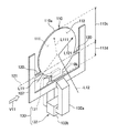
図3は、図1及び図2に模式的に示されている反射板及び駆動部を詳細に示す図であり、図4は、図3に示されている反射板及び駆動部を、図中の矢印V11方向から見た側面図である。 FIG. 3 is a view showing in detail the reflector and the driver shown schematically in FIGS. 1 and 2, and FIG. 4 shows the reflector and the driver shown in FIG. 5 is a side view as viewed from the direction of arrow V11.
反射板110は、円板部110aと矩形板部110bとを有しており、円板部110aの両面に金もしくはアルミニウム等の蒸着により第1反射面111及び第2反射面112が形成されている。この反射板110における円板部110aが、第1支持部120によって、フレーム107に対して、反射板110の面方向に延在する第1回動軸121を中心に回動可能に支持されている。反射板110、第1支持部120、及びフレーム107は、シリコン材で一体に形成されている。
The
フレーム107は、反射板110との間に間隙を開けて反射板110を囲むように、反射板110の面内方向に延在する四角枠である。ただし、フレーム107は、図3及び図4における上方側となる、第1光源101からの照射光L11及び第2光源102からの照射光L12それぞれが反射された反射光L111,L121の出射側を除いて反射板110を囲んでいる。なお、フレーム107の形状は、四角には限定されず、任意の形状とすることができる。
The
第1支持部120は、反射板110とフレーム107との間の間隙に設けられている。第1支持部120は、面方向について反射板110を両側から支持し、この反射板110の第1回動軸121を定めるように一対が設けられている。反射板110は、この一対の第1回動軸121によってフレーム107に連結されており、一対の第1支持部120は、第1回動軸121を中心に捩れるトーションバーとなっている。
The
駆動部130は、第1磁気素子131及び第1磁気アクチュエータ132を有している。第1磁気素子131は、反射板110における第1回動軸121とずれた位置、具体的には反射板110の矩形板部110bに取り付けられる永久磁石である。第1磁気アクチュエータ132は、第1磁気素子131に対して磁気を加えて、第1回動軸121を中心に反射板110を回動させる。
The
ここで、本実施例では、第1回動軸121が、反射板110を、第1回動軸121に対する直交方向について長さが異なる2つの領域110c,110dに二分する。駆動部130における第1磁気素子131は、長さが短い方の領域110dに位置する矩形板部110bに取り付けられている。
Here, in the present embodiment, the first
第1磁気アクチュエータ132は、第1磁気素子131に磁気を加える位置に1つ設けられた電磁石であり、ヨーク132aとコイル132bとを備えている。この第1磁気アクチュエータ132が、第1磁気素子131に磁気を加えて、この第1磁気素子131を第1回動軸121を中心に反射板110を回動させる方向に動かす。
The first
第1磁気素子131は永久磁石であり、常時に磁界を発している。この第1磁気素子131に対し、第1磁気アクチュエータ132が磁界を発生したとすると、これら2つの磁界の相互間の反発と吸引とにより、第1磁気素子131には駆動力が生じる。この駆動力により、反射板110は、第1支持部120で定められる第1回動軸121を中心に回動することとなる。このときの回動量は、不図示の制御部により第1磁気アクチュエータ132が発生する磁界の強さを制御することで調整される。また、回動方向は、第1磁気アクチュエータ132が発生する磁界の向きを制御することで調整される。
The first
図1及び図2に示されている光走査装置1では、駆動部130が反射板110を上記のように回動させながら反射板110が照射光L11,L12を反射することで、第1走査対象領域AL11及び第2走査対象領域AL12が走査されることとなる。
In the
本実施例の光走査装置1によれば、反射板110の第1反射面111及び第2反射面112で反射された2つの照射光L11,L12が、反射板110の回動によって第1走査対象領域AL11及び第2走査対象領域AL12を走査することとなる。これにより、第1走査対象領域AL11及び第2走査対象領域AL12を足し合わせた広い走査対象領域を走査することができる。そして、このような広い走査対象領域が、両面反射タイプの1枚の反射板110を用いた1台の光走査装置1で実現されていることから、設置スペースを抑えることができる。
According to the
ここで、本実施例の光走査装置1では、駆動部130は、永久磁石である第1磁気素子131と、電磁石である第1磁気アクチュエータ132と、を有している。これにより、第1磁気アクチュエータ132で第1磁気素子131を磁気駆動するという簡単な構造で反射板110を確実に回動させることができるので好適である。
Here, in the
また、本実施例の光走査装置1では、反射板110において第1回動軸121によって二分される2つの領域110c,110dのうち、長さが短い方の領域110dに第1磁気素子131が取り付けられている。
Further, in the
これにより、2つの領域110c,110dのうちの長い方の領域110cについて、第1磁気素子131の駆動量に対して、第1回動軸121を中心とした大きな回動量を得ることができる。照射光L11,L12や戻り光L13,L14は、第1磁気素子131を避けて、この長い方の領域110cで反射されることとなる。その結果、第1磁気素子131の駆動量に対して大きな走査量を得ることができるので、一層広い走査対象領域を走査することができる。
As a result, in the longer one of the two
また、本実施例の光走査装置1は、第1光源101及び第2光源102からの照射光L11,L12それぞれが反射された反射光L111,L121の出射側を除いて反射板110を囲むフレーム107を更に備えている。そして、第1支持部120は、反射板110とフレーム107との間の間隙に設けられている。
The
これにより、反射板110を所定の取付け箇所に、上記のフレーム107を利用することで容易に取り付けることができる。そして、そのフレーム107が、上記の反射光L111,L121の出射側を除いて反射板110を囲むように面内方向に延在する。このため、反射光L111,L121や戻り光L13,L14を、フレーム107が遮ることで走査可能な領域を狭めてしまうといった事態を回避することができる。
Thus, the
また、本実施例の光走査装置1によれば、第1走査対象領域AL11及び第2走査対象領域AL12それぞれについての走査結果が、第1受光素子103及び第2受光素子104での検出結果という数値データとして取得される。このため、その走査結果を、様々な処理装置での利用に供することができる。
Further, according to the
次に第2実施例について説明する。この第2実施例は、反射板の支持構造及び駆動部が、上述した第1実施例とは異なっている。一方で、光走査装置における他の構成は、図1及び図2に示されている第1実施例の光走査装置1と同じである。以下では、第2実施例について、第1実施例との相違点である反射板の支持構造及び駆動部に注目して説明を行ない、同一点である光走査装置の構成については説明を割愛する。
Next, a second embodiment will be described. The second embodiment differs from the first embodiment in the support structure of the reflector and the driving unit. On the other hand, the other configuration of the optical scanning device is the same as that of the
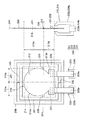
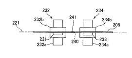
図5は、第2実施例における反射板の支持構造及び駆動部を示した斜視図である。また、図6は、図5に示されている反射板の支持構造及び駆動部を、図中の矢印V21方向から見た平面図、及び、その支持構造及び駆動部の側面図である。また、図7は、図5に示されている反射板の支持構造及び駆動部を、図中の矢印V22方向から見た正面図である。 FIG. 5 is a perspective view showing a support structure and a driving unit of the reflector in the second embodiment. FIG. 6 is a plan view of the support structure and the drive unit of the reflection plate shown in FIG. 5 as viewed from the direction of arrow V21 in the figure, and a side view of the support structure and the drive unit. FIG. 7 is a front view of the support structure and the driving unit of the reflector shown in FIG. 5, as viewed from the direction of arrow V22 in the figure.
まず、本実施例では、反射板210が、上述した第1実施例と同様に、両面のうちの一方に第1反射面211が形成され他方に第2反射面212が形成された両面反射タイプの反射板となっている。そして、この反射板210が、第1実施例と同様の第1支持部220と、第2支持部240と、で支持されている。第2支持部240は、一対の第1支持部220で定められる第1回動軸221と直交する方向に延在する第2回動軸241を中心に反射板210を回動可能に支持するように一対が設けられている。本実施例では、反射板210が、一対の第1支持部220及び一対の第2支持部240によって二軸で支持されている。
First, in this embodiment, the
ここで、第1支持部220は、反射板210との間に間隙を開けて、この反射板210を全周に亘って囲むように、反射板210の面方向に延在する四角枠である内フレーム207に対して反射板210を回動可能に支持している。なお、内フレーム207の形状は、四角には限定されず、任意の形状とすることができる。第1支持部220は、反射板210と内フレーム207との間隙に設けられている。
Here, the
他方、第2支持部240は、上記の内フレーム207との間に間隙を開けて、内フレーム207を全周に亘って囲むように、反射板210の面方向に延在する四角枠である外フレーム208に対して内フレーム207を回動可能に支持している。なお、内フレーム208の形状についても、四角には限定されず、任意の形状とすることができる。第2支持部240は、外フレーム208に対して内フレーム207を回動可能に支持することで、反射板210を間接的に支持している。
On the other hand, the
本実施例では、反射板210、内フレーム207、外フレーム208、一対の第1支持部220、一対の第2支持部240、がシリコン材で一体に形成されている。そして、一対の第1支持部220が、第1回動軸221を中心に捩れるトーションバーとなっており、一対の第2支持部240が、第2回動軸241を中心に捩れるトーションバーとなっている。
In this embodiment, the
駆動部230は、第1磁気素子231及び第1磁気アクチュエータ232のセットと、第2磁気素子233及び第2磁気アクチュエータ234のセットと、を有している。第1磁気素子231及び第2磁気素子233は、いずれも永久磁石であって、反射板210において、第1回動軸221に対して互いに同じ側にずれた位置に、相互間に第2回動軸241を挟んで取り付けられる。
The
反射板210は、第1実施例と同様に円板部210aと矩形板部210bとを有している。ただし、本実施例の反射板210における矩形板部210bは、第1実施例の反射板110における矩形板部110bよりも長めに形成されている。本実施例では、この長めに形成された矩形板部210bに、第1磁気素子231及び第2磁気素子233が、相互間に第2回動軸241を挟むように配列されている。
The
また、本実施例では、第1回動軸221が、反射板210を、第1回動軸221に対する直交方向について長さが異なる2つの領域210c,210dに二分する。他方、第2回動軸241は、反射板210を、第2回動軸241に対する直交方向について互いに同等な2つの領域210eに二等分する。第1磁気素子231及び第2磁気素子233は、長さが短い方の領域210d、具体的には矩形板部210bが第2回動軸241で二等分された2つの領域部分に、それぞれ取り付けられている。
In the present embodiment, the
第1磁気アクチュエータ232は、第1磁気素子231に対して磁気を加えて、第1回動軸221を中心に反射板210を回動させる電磁石であり、ヨーク232aとコイル232bとを備えている。また、第2磁気アクチュエータ234は、第2磁気素子233に対して磁気を加えて、第1回動軸221を中心に反射板210を回動させる電磁石であって、ヨーク234aとコイル234bとを備えている。
The first
このとき、第1磁気アクチュエータ232及び第2磁気アクチュエータ234の相互間で、発生させる磁界の強さや向きを制御することで、第2回動軸241を中心に反射板210を回動させるように構成されている。即ち、第1磁気アクチュエータ232及び第2磁気アクチュエータ234は、互いに協働して第1回動軸221及び第2回動軸241それぞれを中心に反射板210を回動させるものとなっている。
At this time, by controlling the strength and direction of the generated magnetic field between the first
以上に説明した第2実施例によっても、上述した第1実施例と同様に、設置スペースを抑えて広い走査対象領域を走査することができることは言うまでもない。 According to the second embodiment described above, it is needless to say that a wide scanning target area can be scanned with a small installation space, similarly to the first embodiment.
また、本実施例によれば、反射板210を、第1回動軸221と第2回動軸241との二軸で回動させ、走査対象領域を二次元的に走査することができる。
Further, according to the present embodiment, it is possible to rotate the
また、本実施例によれば、長さが短い方の領域210dに取り付けられた第1磁気素子231及び第2磁気素子233を駆動することで、第1回動軸221を中心とした反射板210の回動によって一層広い走査対象領域を走査することができる。そして、第1磁気素子231及び第2磁気素子233が、第2回動軸241で二等分された領域210eに取り付けられていることで、第2回動軸241を中心とした反射板210の回動によってバランスよく走査することができる。
Further, according to the present embodiment, by driving the first
次に第3実施例について説明する。この第3実施例も、反射板の支持構造及び駆動部が、上述した第1実施例とは異なっている。一方で、光走査装置における他の構成は、図1及び図2に示されている第1実施例の光走査装置1と同じである。以下では、第3実施例についても、上述の第2実施例と同様、第1実施例との相違点である反射板の支持構造及び駆動部に注目して説明を行ない、同一点である光走査装置の構成については説明を割愛する。
Next, a third embodiment will be described. This third embodiment also differs from the above-described first embodiment in the support structure of the reflector and the drive section. On the other hand, the other configuration of the optical scanning device is the same as that of the
図8は、第3実施例における反射板の支持構造及び駆動部を示した斜視図である。また、図9は、図8に示されている反射板の支持構造及び駆動部を、図中の矢印V31方向から見た平面図、及び、その支持構造及び駆動部の側面図である。 FIG. 8 is a perspective view showing a support structure and a driving unit of the reflection plate in the third embodiment. FIG. 9 is a plan view of the support structure and the drive unit of the reflector shown in FIG. 8 as viewed from the direction of arrow V31 in the figure, and a side view of the support structure and the drive unit.
本実施例でも、反射板310は、上述した第1実施例と同様に、両面のうちの一方に第1反射面311が形成され他方に第2反射面312が形成された両面反射タイプの反射板となっている。そして、この反射板310が、第1実施例と同様に、第1反射面311及び第2反射面312での反射光の出射側を除いて反射板310を囲むフレーム307に対して一対の第1支持部320によって支持されている。
Also in this embodiment, the
ここで、本実施例では、第1支持部320が、その延在方向について伸縮可能な伸縮構造322を有している。この伸縮構造322は、第1支持部320の一部が延在方向と交差する方向に屈曲を繰り返して形成されたバネ構造である。
Here, in the present embodiment, the
第1支持部320は、第1実施例における第1支持部120と同様に、第1回動軸321を定めるように、反射板310を面方向に挟んで一対が設けられて、反射板310を、第1回動軸321を中心に回動可能に支持している。このとき、各第1支持部320が上記の伸縮構造322を有することで、反射板310は、第1回動軸321と直交する第2回動軸341を中心とした回動についても可能となっている。
Similar to the
一対の第1支持部320が定める第1回動軸321は、反射板310を、第1回動軸321に対する直交方向について長さが異なる2つの領域310c,310dに二分する。
The
また、一対の第1支持部320における伸縮構造322が互いに同等であるために、反射板310は、一対の第1支持部320それぞれの側において互いに同程度に回動可能となっている。このため、伸縮構造322によって可能となる回動の回動軸たる第2回動軸341は、反射板310を、互いに同等な領域310eに二等分するように生じる。
Further, since the expansion and
このように、本実施例では、各々が伸縮構造322を有する一対の第1支持部320によって、反射板310が、第1回動軸321及び第2回動軸341それぞれを中心に二軸で回動可能に支持されている。
As described above, in this embodiment, the pair of
そして、反射板310を二軸で回動させるために、上述した第2実施形態と同様の駆動部330が設けられている。
Further, a
即ち、駆動部330は、第2実施例と同様に、第1磁気素子331及び第1磁気アクチュエータ332のセットと、第2磁気素子333及び第2磁気アクチュエータ334のセットと、を有している。いずれも永久磁石である第1磁気素子331及び第2磁気素子333が、円板部310aと矩形板部310bとを有する反射板310における矩形板部310bに、相互間に第2回動軸341を挟んで取り付けられる。
That is, the driving
第1磁気アクチュエータ332は、第1磁気素子331に対して磁気を加えて、第1回動軸321を中心に反射板210を回動させる電磁石であり、ヨーク332aとコイル332bとを備えている。また、第2磁気アクチュエータ334は、第2磁気素子333に対して磁気を加えて、第1回動軸321を中心に反射板210を回動させる電磁石であって、ヨーク334aとコイル334bとを備えている。そして、これらの第1磁気アクチュエータ332及び第2磁気アクチュエータ334が、互いに協働して第1回動軸321及び第2回動軸341それぞれを中心に反射板310を回動させるものとなっている。
The first
以上に説明した第3実施例によっても、上述した第1実施例と同様に、設置スペースを抑えて広い走査対象領域を走査することができることは言うまでもない。 According to the third embodiment described above, it is needless to say that a wide scanning target area can be scanned with a small installation space as in the first embodiment.
また、本実施例によれば、反射板310を支持する第1支持部320に伸縮構造322を持たせることで、反射板310を第1回動軸321と第2回動軸341との二軸で回動させることができる。つまり、本実施例によっても、上述した第2実施例と同様に走査対象領域を二次元的に走査することができる。
Further, according to the present embodiment, by providing the
尚、本発明は、以上に説明した実施例に限定されるものではなく、本発明の目的が達成できる他の構成等を含み、以下に示すような変形等も本発明に含まれる。 It should be noted that the present invention is not limited to the embodiments described above, but includes other configurations that can achieve the object of the present invention, and also includes the following modifications and the like.
例えば、上述した第1〜第3実施例では、本発明にいう第1磁気素子の一例として永久磁石の第1磁気素子131,231,331が例示されている。同様に、本発明にいう第2磁気素子の一例として、永久磁石の第2磁気素子232,332が例示されている。しかしながら、本発明にいう第1磁気素子や第2磁気素子は、これらに限るものではなく、例えば電流が流されて磁界を受けると駆動力が生じるコイル等であってもよい。この場合、このコイルを動かす磁気アクチュエータは永久磁石であってもよい。
For example, in the above-described first to third embodiments, the first
また、上述した第1〜第3実施例では、本発明にいう反射板の一例として円板部110a,210a,310aと矩形板部110b,210b,310bとを備えた反射板110,310が例示されている。しかしながら、本発明にいう反射板はこれらに限るものではない。本発明にいう反射板は、両面に反射領域が形成されたものであれば、単純な円板状であっても矩形板状であってもよく、その具体的形状を問うものではない。
In the above-described first to third embodiments, the
また、上述した第1〜第3実施例では、本発明にいう第1磁気素子や第2磁気素子の各一例として、反射板110,210,310の一方の面に取り付けられた第1磁気素子131,231,331や第2磁気素子233,333が例示されている。しかしながら、本発明にいう第1磁気素子や第2磁気素子はこれらに限るものではない。本発明にいう第1磁気素子や第2磁気素子は、例えば反射板の両方の面に取り付けてもよい。又は、反射板の磁石取付位置に開口を設け、そこに第1磁気素子や第2磁気素子をはめ込んでもよい。この場合、反射板の両方の面に第1磁気素子や第2磁気素子が現れることになる。第1磁気素子や第2磁気素子を両面に取り付けた場合、又は開口にはめ込んだ場合は、反射板が縦になるように取り付けても、反射板の回動軸に対してバランスがとれた状態にできる。このため、例えば非駆動時において反射板が回動して一方に傾いてしまうことがない。
In the above-described first to third embodiments, the first magnetic element attached to one surface of each of the
また、上述した第1〜第3実施例では、本発明にいう第1磁気素子や第2磁気素子の各一例として、長手方向を有する長方形の形状の第1磁気素子131,231,331や第2磁気素子233,333が例示されている。しかしながら、本発明にいう第1磁気素子や第2磁気素子はこれらに限るものではない。本発明にいう第1磁気素子や第2磁気素子は、反射板を回動駆動させるのに十分な力が得られるのであれば、磁気素子の形状やサイズは任意に設定してよく、例えば正方形に形成した磁気素子を用いることもできる。
In the above-described first to third embodiments, as the first magnetic element and the second magnetic element according to the present invention, for example, the first
また、上述した第2及び第3実施例では、本発明にいう第1磁気素子や第2磁気素子の各一例として、互いに別体に形成され、個別に反射板210,310に取り付けられた第1磁気素子231,331や第2磁気素子233,333が例示されている。しかしながら、本発明にいう第1磁気素子や第2磁気素子はこれらに限るものではない。本発明にいう第1磁気素子や第2磁気素子は、例えば、長尺に形成された1個の磁石を反射板に取り付け、その一端側を第1磁気素子として使用し、他端側を第2磁気素子として使用するものであってもよい。
In the above-described second and third embodiments, each of the first magnetic element and the second magnetic element according to the present invention is formed separately from each other and individually attached to the
また、上述した第2及び第3実施例では、本発明にいう駆動部の一例として、反射板210,310の二軸回動のために、第1磁気素子231,331や第2磁気素子233,333という2つの磁気素子を横並びに配列した駆動部230,330が例示されている。また、各実施例の駆動部230,330では、これら2つの磁気素子を駆動すべく第1磁気アクチュエータ232,332や第2磁気アクチュエータ234,334が横並びに配列されている。しかしながら、本発明にいう駆動部は、二軸回動のためのものであっても、第2及び第3実施例に例示された構造に限るものではなく、磁気素子や磁気アクチュエータの数や配置は任意に設定し得る。例えば、反射板や、これを囲むフレームに、反射面を三方から囲むように3つの磁気素子を配置し、各磁気素子を駆動すべく3つの磁気アクチュエータを設けることとしてもよい。この場合、1つの磁気素子と磁気アクチュエータで1つの回動軸を中心として反射板を回動させ、他の2つの磁気素子と磁気アクチュエータでもう1つの回動軸を中心として反射板を回動させることとなる。このように、本発明にいう駆動部は、第1回動軸を中心に前記反射板を回動させるものであれば、他の回動軸を中心とした回動構造の有無を含めて、その具体的な構成を問うものではない。
In the above-described second and third embodiments, as an example of the driving unit according to the present invention, the first
1 光走査装置
101 第1光源
102 第2光源
103 第1受光素子
104 第2受光素子
105 第1光学素子
106 第2光学素子
107,307 フレーム
110,210,310 反射板
110a,210a,310a 円板部
110b,210b,310b 矩形板部
110c,110d,210c,210d,210e,310c,310d,310e領域
111,211,311 第1反射面
112,212,312 第2反射面
120,220,320 第1支持部
121,221,321 第1回動軸
130,230,330 駆動部
131,231,331 第1磁気素子
132,232,332 第1磁気アクチュエータ
132a,232a,234a,332a,334a ヨーク
132b,232b,234b、332b、334b コイル
207 内フレーム
208 外フレーム
233,333 第2磁気素子
234,334 第2磁気アクチュエータ
240 第2支持部
241,341 第2回動軸
322 伸縮構造
AL11 第1走査対象領域
AL12 第2走査対象領域
D11 回動方向
L11,L12 照射光
L111,L121 反射光
L13,L14 戻り光
P11 第1限界位置
P12 第2限界位置
DESCRIPTION OF
Claims (8)
第2光源と、
両面のうちの一方に前記第1光源からの照射光を反射する第1反射面が形成され、他方に前記第2光源からの照射光を反射する第2反射面が形成された反射板と、
前記反射板の面方向に延在する第1回動軸を中心に前記反射板を回動可能に支持する第1支持部と、
前記第1回動軸を中心に前記反射板を回動させる駆動部と、
を備えることを特徴とする光走査装置。 A first light source;
A second light source;
A reflector having a first reflection surface formed on one of both surfaces for reflecting irradiation light from the first light source, and a second reflection surface formed on the other surface for reflecting irradiation light from the second light source;
A first support unit that rotatably supports the reflection plate around a first rotation axis extending in a surface direction of the reflection plate;
A drive unit for rotating the reflection plate about the first rotation axis;
An optical scanning device comprising:
前記第1磁気素子が、前記長さが短い方の領域に取り付けられていることを特徴とする請求項2に記載の光走査装置。 The first rotation axis bisects the reflection plate into two regions having different lengths in a direction orthogonal to the first rotation axis;
The optical scanning device according to claim 2, wherein the first magnetic element is attached to the shorter area.
前記第1支持部は、前記反射板と前記フレームとの間の間隙に設けられていることを特徴とする請求項2又は3に記載の光走査装置。 A gap is formed between the reflector and the reflector, and the reflector and the irradiating light from the first light source and the irradiating light from the second light source are respectively surrounded by the reflector except for the emission side of the reflected light. Further comprising a frame extending in the in-plane direction,
4. The optical scanning device according to claim 2, wherein the first support portion is provided in a gap between the reflection plate and the frame. 5.
前記駆動部は、前記反射板において、前記第1回動軸に対して前記第1磁気素子と同じ側にずれた位置に、当該第1磁気素子との間に前記第2回動軸を挟んで取り付けられる第2磁気素子、及び、当該第2磁気素子に磁気を加え、前記第1磁気アクチュエータと協働して前記第1回動軸及び前記第2回動軸それぞれを中心に前記反射板を回動させる第2磁気アクチュエータ、を有していることを特徴とする請求項2又は3に記載の光走査装置。 A second support portion that rotatably supports the reflection plate around a second rotation axis extending in a direction different from the first rotation axis;
The drive unit sandwiches the second rotation axis between the reflection plate and the first magnetic element at a position shifted to the same side as the first magnetic element with respect to the first rotation axis. A magnetic element attached to the second magnetic element, and magnetism applied to the second magnetic element, and the reflection plate is provided around the first and second rotation axes in cooperation with the first magnetic actuator. 4. The optical scanning device according to claim 2, further comprising a second magnetic actuator that rotates the light scanning device. 5.
前記駆動部は、前記反射板において、前記第1回動軸に対して前記第1磁気素子と同じ側にずれた位置に、当該第1磁気素子との間に前記第2回動軸を挟んで取り付けられる第2磁気素子、及び、当該第2磁気素子に磁気を加え、前記第1磁気アクチュエータと協働して前記第1回動軸及び前記第2回動軸それぞれを中心に前記反射板を回動させる第2磁気アクチュエータ、を有していることを特徴とする請求項2〜4のうち何れか一項に記載の光走査装置。 Since the first support portion has a telescopic structure that can expand and contract in the direction in which the first support portion extends, the first support portion can be rotated around a second rotation axis that extends in a direction different from the first rotation axis. To support the reflector,
The drive unit sandwiches the second rotation axis between the reflection plate and the first magnetic element at a position shifted to the same side as the first magnetic element with respect to the first rotation axis. A second magnetic element attached to the second magnetic element, and magnetism applied to the second magnetic element, and the reflection plate is provided around the first and second rotation axes in cooperation with the first magnetic actuator. 5. The optical scanning device according to claim 2, further comprising a second magnetic actuator configured to rotate the optical scanning device. 6.
前記第2回動軸が、前記反射板を、前記第2回動軸に対する直交方向について二等分し、
前記第1磁気素子及び前記第2磁気素子は、前記長さが短い方の領域が前記第2回動軸で二等分された2つの領域部分に、それぞれ取り付けられていることを特徴とする請求項5又は6に記載の光走査装置。 The first rotation axis bisects the reflection plate into two regions having different lengths in a direction orthogonal to the first rotation axis;
The second rotation axis bisects the reflection plate in a direction orthogonal to the second rotation axis;
The first magnetic element and the second magnetic element are characterized in that the shorter area is respectively attached to two area parts bisected by the second rotation axis. The optical scanning device according to claim 5.
前記光とは異なる光路の光を検出する第2受光素子と、
前記第1光源からの前記照射光で第1走査対象領域が走査された結果、当該第1走査対象領域から戻って前記第1反射面で反射された戻り光を前記第1受光素子に導光する第1光学素子と、
前記第2光源からの前記照射光で第2走査対象領域が走査された結果、当該第2走査対象領域から戻って前記第2反射面で反射された戻り光を前記第2受光素子に導光する第2光学素子と、
を備えることを特徴とする請求項1〜7のうち何れか一項に記載の光走査装置。 A first light receiving element for detecting light,
A second light receiving element that detects light in an optical path different from the light,
As a result of scanning the first scan target area with the irradiation light from the first light source, the return light reflected from the first reflection surface returning from the first scan target area is guided to the first light receiving element. A first optical element,
As a result of scanning the second scan target area with the irradiation light from the second light source, the return light reflected from the second reflection surface after returning from the second scan target area is guided to the second light receiving element. A second optical element,
The optical scanning device according to claim 1, further comprising:
Priority Applications (3)
| Application Number | Priority Date | Filing Date | Title |
|---|---|---|---|
| JP2018122611A JP2020003629A (en) | 2018-06-28 | 2018-06-28 | Optical scanner |
| JP2022164753A JP2022186801A (en) | 2018-06-28 | 2022-10-13 | optical scanner |
| JP2023208968A JP2024022659A (en) | 2018-06-28 | 2023-12-12 | optical scanning device |
Applications Claiming Priority (1)
| Application Number | Priority Date | Filing Date | Title |
|---|---|---|---|
| JP2018122611A JP2020003629A (en) | 2018-06-28 | 2018-06-28 | Optical scanner |
Related Child Applications (1)
| Application Number | Title | Priority Date | Filing Date |
|---|---|---|---|
| JP2022164753A Division JP2022186801A (en) | 2018-06-28 | 2022-10-13 | optical scanner |
Publications (1)
| Publication Number | Publication Date |
|---|---|
| JP2020003629A true JP2020003629A (en) | 2020-01-09 |
Family
ID=69099956
Family Applications (3)
| Application Number | Title | Priority Date | Filing Date |
|---|---|---|---|
| JP2018122611A Pending JP2020003629A (en) | 2018-06-28 | 2018-06-28 | Optical scanner |
| JP2022164753A Ceased JP2022186801A (en) | 2018-06-28 | 2022-10-13 | optical scanner |
| JP2023208968A Ceased JP2024022659A (en) | 2018-06-28 | 2023-12-12 | optical scanning device |
Family Applications After (2)
| Application Number | Title | Priority Date | Filing Date |
|---|---|---|---|
| JP2022164753A Ceased JP2022186801A (en) | 2018-06-28 | 2022-10-13 | optical scanner |
| JP2023208968A Ceased JP2024022659A (en) | 2018-06-28 | 2023-12-12 | optical scanning device |
Country Status (1)
| Country | Link |
|---|---|
| JP (3) | JP2020003629A (en) |
Cited By (2)
| Publication number | Priority date | Publication date | Assignee | Title |
|---|---|---|---|---|
| JP2021162661A (en) * | 2020-03-31 | 2021-10-11 | パイオニア株式会社 | Light deflector |
| JP2024022659A (en) * | 2018-06-28 | 2024-02-16 | パイオニア株式会社 | optical scanning device |
Citations (4)
| Publication number | Priority date | Publication date | Assignee | Title |
|---|---|---|---|---|
| JPH03215815A (en) * | 1990-01-19 | 1991-09-20 | Nec Corp | Scanning mirror driving device |
| JP2008304667A (en) * | 2007-06-07 | 2008-12-18 | Seiko Epson Corp | Actuator, optical scanner and image forming apparatus |
| JP2009210947A (en) * | 2008-03-05 | 2009-09-17 | Canon Inc | Optical scanning device and optical equipment using the same |
| JP2012117996A (en) * | 2010-12-03 | 2012-06-21 | Fujitsu Ltd | Distance measuring apparatus and distance measuring method |
Family Cites Families (13)
| Publication number | Priority date | Publication date | Assignee | Title |
|---|---|---|---|---|
| EP0660255A3 (en) * | 1993-12-24 | 1998-04-08 | Opticon Sensors Europe B.V. | Oscillation bar code reader |
| JPH08240782A (en) * | 1995-03-02 | 1996-09-17 | Omron Corp | Optical scanner, optical sensor device, code information reading device, and code information reading method |
| JPH1097819A (en) * | 1996-09-20 | 1998-04-14 | Fujikura Ltd | Membrane switch |
| JP3129219B2 (en) * | 1997-01-14 | 2001-01-29 | 日本電気株式会社 | Optical scanner |
| JP4244649B2 (en) * | 2003-02-10 | 2009-03-25 | 株式会社デンソー | Optical element |
| FR2859541B1 (en) * | 2003-09-08 | 2005-10-14 | Commissariat Energie Atomique | MICRO-MIRROR ELECTRICALLY ACTIVATED IN ROTATION |
| JP2008015256A (en) * | 2006-07-06 | 2008-01-24 | Toyota Central Res & Dev Lab Inc | Optical deflector |
| JP2011053253A (en) * | 2009-08-31 | 2011-03-17 | Brother Industries Ltd | Optical scanner |
| DE102012208117B4 (en) * | 2012-05-15 | 2023-10-05 | Robert Bosch Gmbh | Micromechanical component |
| JP6201528B2 (en) * | 2012-11-15 | 2017-09-27 | 株式会社リコー | Optical deflection apparatus, image forming apparatus, head-up display, and vehicle |
| JP5996774B2 (en) * | 2013-03-11 | 2016-09-21 | インテル コーポレイション | Method and apparatus for providing field of view of MEMS scanning mirror |
| JP2015025901A (en) * | 2013-07-25 | 2015-02-05 | 船井電機株式会社 | Laser scanning apparatus |
| JP2020003629A (en) * | 2018-06-28 | 2020-01-09 | パイオニア株式会社 | Optical scanner |
-
2018
- 2018-06-28 JP JP2018122611A patent/JP2020003629A/en active Pending
-
2022
- 2022-10-13 JP JP2022164753A patent/JP2022186801A/en not_active Ceased
-
2023
- 2023-12-12 JP JP2023208968A patent/JP2024022659A/en not_active Ceased
Patent Citations (4)
| Publication number | Priority date | Publication date | Assignee | Title |
|---|---|---|---|---|
| JPH03215815A (en) * | 1990-01-19 | 1991-09-20 | Nec Corp | Scanning mirror driving device |
| JP2008304667A (en) * | 2007-06-07 | 2008-12-18 | Seiko Epson Corp | Actuator, optical scanner and image forming apparatus |
| JP2009210947A (en) * | 2008-03-05 | 2009-09-17 | Canon Inc | Optical scanning device and optical equipment using the same |
| JP2012117996A (en) * | 2010-12-03 | 2012-06-21 | Fujitsu Ltd | Distance measuring apparatus and distance measuring method |
Cited By (3)
| Publication number | Priority date | Publication date | Assignee | Title |
|---|---|---|---|---|
| JP2024022659A (en) * | 2018-06-28 | 2024-02-16 | パイオニア株式会社 | optical scanning device |
| JP2021162661A (en) * | 2020-03-31 | 2021-10-11 | パイオニア株式会社 | Light deflector |
| JP7469940B2 (en) | 2020-03-31 | 2024-04-17 | パイオニア株式会社 | Optical Deflector |
Also Published As
| Publication number | Publication date |
|---|---|
| JP2024022659A (en) | 2024-02-16 |
| JP2022186801A (en) | 2022-12-15 |
Similar Documents
| Publication | Publication Date | Title |
|---|---|---|
| JP2024022659A (en) | optical scanning device | |
| JP3548556B2 (en) | X-ray diffractometer | |
| JP6053277B2 (en) | Magnetic actuator and micromirror and mirror system using the same | |
| JP2024094398A (en) | Actuated reflector, optical scanning device, and mirror actuator | |
| CN101681020B (en) | Object detector | |
| JP5657008B2 (en) | Apparatus and method for deflecting a light beam in two different directions and a scanning microscope | |
| CN101681019A (en) | Optical scanning actuator | |
| JPWO2008152979A1 (en) | Optical scanning sensor | |
| JP2024026611A (en) | distance measuring device | |
| JP4532478B2 (en) | X-ray optical system with adjustable convergence | |
| CN110308168B (en) | X-ray diffraction apparatus | |
| JP7281880B2 (en) | optical scanner | |
| CN108226937A (en) | For the laser radar sensor of detection object | |
| JP5567807B2 (en) | Scan antenna | |
| JP4619180B2 (en) | Optical scanning actuator | |
| CN113777561B (en) | RCS reflector system capable of changing polarization characteristics | |
| JP2016080899A (en) | Optical scanner | |
| JP2009265479A (en) | Optical deflector and method of driving the same | |
| JP7370187B2 (en) | mirror actuator | |
| WO2025028387A1 (en) | Automatized alignment of x-ray optics and x-ray beams | |
| JP2007073133A5 (en) | ||
| JP2012104813A (en) | Polarization actuator | |
| WO2019151092A1 (en) | Scanning device and distance measuring device | |
| JPH0626971Y2 (en) | Optical disk device | |
| US20250035886A1 (en) | Oscillating mirrors for lidar |
Legal Events
| Date | Code | Title | Description |
|---|---|---|---|
| A621 | Written request for application examination |
Free format text: JAPANESE INTERMEDIATE CODE: A621 Effective date: 20210513 |
|
| A977 | Report on retrieval |
Free format text: JAPANESE INTERMEDIATE CODE: A971007 Effective date: 20220214 |
|
| A131 | Notification of reasons for refusal |
Free format text: JAPANESE INTERMEDIATE CODE: A131 Effective date: 20220308 |
|
| A521 | Request for written amendment filed |
Free format text: JAPANESE INTERMEDIATE CODE: A523 Effective date: 20220427 |
|
| A02 | Decision of refusal |
Free format text: JAPANESE INTERMEDIATE CODE: A02 Effective date: 20220719 |