JP2020004754A - Semiconductor optical element and optical transmission module - Google Patents
Semiconductor optical element and optical transmission module Download PDFInfo
- Publication number
- JP2020004754A JP2020004754A JP2018119555A JP2018119555A JP2020004754A JP 2020004754 A JP2020004754 A JP 2020004754A JP 2018119555 A JP2018119555 A JP 2018119555A JP 2018119555 A JP2018119555 A JP 2018119555A JP 2020004754 A JP2020004754 A JP 2020004754A
- Authority
- JP
- Japan
- Prior art keywords
- layer
- mesa structure
- optical device
- semiconductor optical
- semiconductor
- Prior art date
- Legal status (The legal status is an assumption and is not a legal conclusion. Google has not performed a legal analysis and makes no representation as to the accuracy of the status listed.)
- Granted
Links
Images




Landscapes
- Semiconductor Lasers (AREA)
Abstract
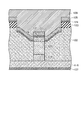
【課題】メサ構造上部が埋め込み層から突出する埋め込みヘテロ構造型半導体レーザにおいて、埋め込み層から突出するメサ構造上部の側面が電極層から受ける応力を低減する。【解決手段】半導体光素子は、第一導電型を有する基板118と、基板118上に設けられる活性層119、活性層119上に設けられて第一導電型とは異なる第二導電型を有するクラッド層120、及びクラッド層120上に設けられる第二導電型を有するコンタクト層121を含むメサ構造と、基板118上に設けられ、かつ、メサ構造を埋め込む埋め込み層122と、コンタクト層121上と埋め込み層122上に設けられる少なくとも2つの層を含む電極層116、を有する。半導体光素子では、メサ構造の上部は埋め込み層122から露出し、メサ構造上と埋め込み層122上に堆積される電極層116のうちの一の層及び/又は一の層上に堆積される他の層は、メサ構造の上部の側壁で分離する。【選択図】図4PROBLEM TO BE SOLVED: To reduce a stress received from an electrode layer on a side surface of an upper part of a mesa structure protruding from an embedded layer in an embedded heterostructure type semiconductor laser in which the upper part of the mesa structure protrudes from the embedded layer. A semiconductor optical device has a substrate 118 having a first conductive type, an active layer 119 provided on the substrate 118, and a second conductive type provided on the active layer 119 and different from the first conductive type. A mesa structure including a clad layer 120 and a contact layer 121 having a second conductive type provided on the clad layer 120, an embedded layer 122 provided on the substrate 118 and embedding the mesa structure, and a contact layer 121. It has an electrode layer 116, which includes at least two layers provided on the embedded layer 122. In semiconductor optical elements, the upper part of the mesa structure is exposed from the embedded layer 122, and is deposited on one layer and / or one layer of the electrode layers 116 deposited on the mesa structure and the embedded layer 122. Layers are separated by the upper sidewall of the mesa structure. [Selection diagram] FIG. 4
Description
本発明は、半導体光素子及びその製造方法並びに光送信モジュールに関する。 The present invention relates to a semiconductor optical device, a method for manufacturing the same, and an optical transmission module.
半導体光素子の一つである半導体レーザは、光通信、情報処理、光源など、様々な用途で利用されており、低コスト、低消費電力、小型、高光出力、高信頼性が求められている。一般的に、半導体光素子は、pn接合を構成する半導体結晶と、電極を構成する金属を有する。 Semiconductor lasers, one of the semiconductor optical devices, are used in various applications such as optical communication, information processing, and light sources, and are required to have low cost, low power consumption, small size, high optical output, and high reliability. . Generally, a semiconductor optical device has a semiconductor crystal forming a pn junction and a metal forming an electrode.
半導体光素子のなかでも埋め込みヘテロ構造(BH:Buried−Heterostructure)は、pn接合を構成する半導体結晶をメサ構造にし、該メサ構造の側部を半絶縁性半導体の埋め込み層で埋め込んでいる。そのため電極はメサ構造の上面(コンタクト層の上部の露出した面)と埋め込み層の上面にわたって配置される。 Among the semiconductor optical devices, a buried heterostructure (BH) has a semiconductor crystal forming a pn junction in a mesa structure, and a side portion of the mesa structure is buried with a buried layer of a semi-insulating semiconductor. Therefore, the electrodes are arranged over the upper surface of the mesa structure (the exposed surface above the contact layer) and the upper surface of the embedded layer.
半導体光素子の電極を構成する金属は、電子ビーム蒸着等の高温プロセスによって半導体結晶層上に成膜されることが一般的である。成膜された金属が高温から室温へ降温すると、半導体と金属の熱膨張係数の差によって半導体結晶に応力が発生する。このような応力は半導体光素子の性能に悪影響を及ぼすことが知られている。そのため、これまでこのような応力を緩和するための様々な提案がなされてきた。 Generally, a metal constituting an electrode of a semiconductor optical device is formed on a semiconductor crystal layer by a high-temperature process such as electron beam evaporation. When the temperature of the formed metal drops from a high temperature to room temperature, stress is generated in the semiconductor crystal due to a difference in thermal expansion coefficient between the semiconductor and the metal. It is known that such stress adversely affects the performance of the semiconductor optical device. Therefore, various proposals have been made so far to alleviate such stress.
特許文献1では、二重チャネル平面埋め込みヘテロ構造(DC−PBH:Double−Channel Planar Buried Heterostructure)型半導体レーザにおいて、電極を構成するPtによる半導体結晶に生じる応力と信頼性の関係が報告されている。例えば特許文献1では、TiPtAuオーミック電極を、メサ構造の両外部近傍でメサ部に沿って切断することが提案されている。
In
特許文献2では、リッジ型半導体レーザにおける、金属による半導体結晶の応力とレーザ活性層又は光吸収層の特性ばらつきの関係が報告されている。例えば特許文献2では、メサ構造上の電極に応力低減用スリットを加えることが提案されている。 Patent Document 2 reports the relationship between stress of a semiconductor crystal due to metal and variation in characteristics of a laser active layer or a light absorption layer in a ridge type semiconductor laser. For example, Patent Document 2 proposes to add a slit for reducing stress to an electrode on a mesa structure.
特許文献3では、リッジ型半導体レーザにおいて電極によるリッジ直下の活性層の応力を緩和することが提案されている。例えば特許文献3では、リッジ上部のコンタクト層の側壁部分とコンタクト直下の半導体リッジ構造の側壁部分に空洞を設ける構造が提案されている。 Patent Literature 3 proposes that in a ridge-type semiconductor laser, stress in an active layer immediately below the ridge due to an electrode is relaxed. For example, Patent Document 3 proposes a structure in which a cavity is provided in a sidewall portion of a contact layer above a ridge and a sidewall portion of a semiconductor ridge structure immediately below a contact.
特許文献4では、窒化物半導体レーザのリッジ型構造において、電極による窒化物半導体層、およびリッジの応力と信頼性の関係が報告されている。例えば特許文献4では、リッジ基底部において、半導体層上の保護膜と、保護膜上の電極の間に空隙を設ける構造が提案されている。 Patent Literature 4 reports a relationship between stress and reliability of a nitride semiconductor layer and a ridge in an ridge structure of a nitride semiconductor laser. For example, Patent Document 4 proposes a structure in which a gap is provided between a protective film on a semiconductor layer and an electrode on the protective film at a ridge base.
前述したBH構造では、メサ構造の上面と埋め込み層の上面は概ね同一面となることが一般的であるが、BH構造の製造プロセスの中には、埋め込み層からメサ構造の上部を突出させるプロセスがある。そのようにメサ構造の一部が埋め込み層から突出する半導体光素子では、突出したメサ構造の一部の側面にも電極が形成される。そのためメサ構造は上面に加えて側面からも電極の応力を感じることになる。結果として、上部が突出したメサ構造は、上部が突出していないメサ構造よりも電極からより大きな影響を受ける。そのためメサ構造の上部が突出したBH構造型半導体レーザにおいては、応力緩和は特に重要であることを我々は見出した。 In the above-described BH structure, the upper surface of the mesa structure and the upper surface of the buried layer are generally substantially the same. However, in the manufacturing process of the BH structure, a process of projecting the upper part of the mesa structure from the buried layer is included. There is. In a semiconductor optical device in which a part of the mesa structure protrudes from the buried layer, an electrode is also formed on a part of the side surface of the protruding mesa structure. Therefore, in the mesa structure, the stress of the electrode is felt not only from the upper surface but also from the side surfaces. As a result, the protruding mesa structure is more affected by the electrodes than the non-protruding mesa structure. Therefore, we have found that stress relaxation is particularly important in a BH structure type semiconductor laser in which the upper part of the mesa structure protrudes.
しかし特許文献1で開示されている応力緩和は、コンタクト層が埋め込み層から露出していないBH構造の応力を緩和している。また特許文献2乃至4で開示されている応力緩和は、リッジ型半導体レーザの応力緩和であってBH構造型半導体レーザの応力緩和ではない。そのため特許文献1乃至4に開示された応力緩和では、BH構造型半導体レーザの応力緩和を十分に実現し得ない恐れがある。
However, the stress relaxation disclosed in
上記の理解に基づき本願発明者等は、特許文献1乃至4に開示された応力緩和について検討した。その結果本願発明者等は、特許文献1乃至4に開示された応力緩和では、コンタクト層が埋め込み層から一部又は全部が露出しているBH構造半導体レーザのSMSR(Side Mode Suppression Ratio)特性に及ぼす悪影響が十分に緩和されないことを発見した。
Based on the above understanding, the present inventors have studied the stress relaxation disclosed in
よって本願発明は、メサ構造上部が埋め込み層から突出するBH構造型半導体レーザにおいて、埋め込み層から突出するメサ構造上部の側面が電極層から受ける応力を低減することを目的とする。 Therefore, an object of the present invention is to reduce the stress applied to the side surface of the mesa structure projecting from the buried layer from the electrode layer in the BH structure type semiconductor laser having the mesa structure projecting from the buried layer.
(1)本願の半導体光素子は、第一導電型を有する基板と、前記基板上に設けられる活性層、該活性層上に設けられて前記第一導電型とは異なる第二導電型を有するクラッド層、及び前記クラッド層上に設けられる第二導電型を有するコンタクト層を含むメサ構造と、前記基板上に設けられ、かつ、前記メサ構造を埋め込む埋め込み層と、前記コンタクト層上と前記埋め込み層上に設けられる少なくとも2つの層を含む電極層、を有する。当該半導体光素子では、前記メサ構造の上部は前記埋め込み層から露出し、前記メサ構造上と前記埋め込み層上に堆積される前記電極層のうちの一の層及び/又は該一の層上に堆積される他の層は、前記メサ構造の上部の側壁で分離する。 (1) The semiconductor optical device of the present application has a substrate having a first conductivity type, an active layer provided on the substrate, and a second conductivity type provided on the active layer and different from the first conductivity type. A mesa structure including a clad layer, and a contact layer having a second conductivity type provided on the clad layer; a buried layer provided on the substrate and embedding the mesa structure; An electrode layer including at least two layers provided on the layer. In the semiconductor optical device, an upper portion of the mesa structure is exposed from the buried layer, and one of the electrode layers and / or one of the electrode layers deposited on the mesa structure and the buried layer is formed on the mesa structure. Other layers to be deposited separate at the upper sidewall of the mesa structure.
(2)(1)の半導体光素子において、前記他の層の厚さが、前記メサ構造の上部が前記埋め込み層から露出している部分の厚さより厚く、前記他の層は前記コンタクト層上から前記埋め込み層上において、連続的に繋がっており、前記一の層は、前記メサ構造の上部の側壁で分離する。 (2) In the semiconductor optical device according to (1), the thickness of the other layer is greater than the thickness of a portion where the upper part of the mesa structure is exposed from the buried layer, and the other layer is on the contact layer. To the buried layer, and the one layer is separated by an upper sidewall of the mesa structure.
(3)(1)の半導体光素子において、前記一の層の厚さが、前記メサ構造の上部が前記埋め込み層から露出している部分の厚さより厚く、前記一の層は前記コンタクト層上から前記埋め込み層上において、連続的に繋がっており、前記他の層は、前記メサ構造の上部の側壁で分離する。 (3) In the semiconductor optical device according to (1), a thickness of the one layer is larger than a thickness of a portion where an upper part of the mesa structure is exposed from the buried layer, and the one layer is on the contact layer. And the buried layer is continuously connected, and the other layer is separated by an upper sidewall of the mesa structure.
(4)(1)の半導体光素子において、前記メサ構造の内、前記埋め込み層から露出している領域は、前記コンタクト層の一部である。 (4) In the semiconductor optical device according to (1), a region of the mesa structure exposed from the buried layer is a part of the contact layer.
(5)(1)の半導体光素子において、前記一の層と前記他の層の厚さの合計は、前記メサ構造の上部が前記埋め込み層から露出している厚さより薄い。 (5) In the semiconductor optical device according to (1), a total thickness of the one layer and the other layer is smaller than a thickness of an upper portion of the mesa structure exposed from the buried layer.
(6)(1)乃至(4)のいずれかの半導体光素子において、前記一の層と前記他の層の厚さの合計は、前記メサ構造の上部が前記埋め込み層から露出している厚さより厚い。 (6) In the semiconductor optical device according to any one of (1) to (4), the total thickness of the one layer and the other layer is a thickness at which an upper part of the mesa structure is exposed from the buried layer. Thicker than
(7)(1)乃至(3)のいずれかの半導体光素子において、前記メサ構造の内、前記埋め込み層から露出している領域は、前記コンタクト層の全部である。 (7) In the semiconductor optical device according to any one of (1) to (3), a region exposed from the buried layer in the mesa structure is the entire contact layer.
(8)(1)乃至(7)のいずれかの半導体光素子において、前記電極層のうちの一の層はTiであり、前記電極層のうちの他の層はPtである。 (8) In the semiconductor optical device according to any one of (1) to (7), one of the electrode layers is Ti, and the other of the electrode layers is Pt.
(9)本願の光送信モジュールは、(1)乃至(8)のいずれかの半導体光素子を備える。 (9) The optical transmission module of the present application includes the semiconductor optical device according to any one of (1) to (8).
(10)本願の光送受信モジュールは、(1)乃至(8)のいずれかの半導体光素子を備える。 (10) The optical transceiver module of the present application includes the semiconductor optical device according to any one of (1) to (8).
本発明は、メサ構造上部が埋め込み層から突出するBH構造型半導体レーザにおいて、埋め込み層から突出するメサ構造上部の側面が電極層から受ける応力を低減させる。 According to the present invention, in a BH structure type semiconductor laser in which an upper portion of a mesa structure protrudes from a buried layer, a stress received from an electrode layer on a side surface of the upper portion of the mesa structure protruding from the buried layer is reduced.
[第1実施形態]
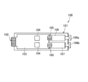
図1は、本願実施形態による光送信モジュールを備える光送受信モジュールを示す。光送受信モジュール100は、筺体101と、筺体101中に設けられる、エッジ・コネクタ102を備えるプリント基板103と、光送信モジュール106(TOSA:Transmitter Optical Sub Assembly)と、光受信モジュール107(ROSA:Receiver Optical Sub Assembly)と、筺体101に取り付けられる光ファイバコネクタ108a,108bを有する。プリント基板103は該プリント基板103上に集積回路104を有する。
[First Embodiment]
FIG. 1 shows an optical transmitting and receiving module including the optical transmitting module according to the embodiment of the present application. The optical transmission /
プリント基板103は、光送信モジュール106及び光受信モジュール107とはフレキシブル基板105によってそれぞれ接続される。光ファイバコネクタ108a,108bは、光送信モジュール106及び光受信モジュール107にそれぞれ光学的に位置合わせされている。
The printed
集積回路104は信号再生機能や増幅機能を有する。光送信モジュール106は電気信号を光信号に変換する機能を有する。光受信モジュール107は光信号を電気信号に変換する機能を有する。
The
エッジ・コネクタ102は、光受信モジュール107からの電気信号をホスト装置(不図示)へ出力し、かつ、ホスト装置(不図示)からの電気信号を光送信モジュール106へ出力する。光ファイバコネクタ108a,108bは光送受信モジュール100の入出力手段として機能する。すなわち、入力光は、光ファイバコネクタ108bに接続される光ファイバ(不図示)を介して光受信モジュール107へ入力され、かつ、出力光は、光ファイバコネクタ108aに接続される光ファイバ(不図示)を介して光送信モジュール106から出力される。
The
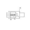
図2は本願実施形態による光送信モジュールを示す。光送信モジュール106は、チップキャリア109と、該チップキャリア109上に搭載された半導体光素子110と、凸レンズ111を有する。
FIG. 2 shows an optical transmission module according to the present embodiment. The
半導体光素子110は光を放出する。凸レンズ111は半導体光素子110から放出された光を平行光又は集束光に変換する。
The semiconductor
図3は本願実施形態による半導体光素子の上面図を示す。図示されている半導体光素子110は電界吸収型光変調器集積分布帰還型レーザ(EA−DFB:Electro−Absorption modulator − Distributed Feedback laser)である。半導体光素子110は、レーザ部112と、導波路部113と、変調器部114と、メサ構造(メサストライプ)115を有する。
FIG. 3 is a top view of the semiconductor optical device according to the present embodiment. The illustrated semiconductor
レーザ部112の上部には電極116が設けられている。電極116は少なくとも2層の金属層を含んでよい。レーザ部112はDFBレーザ素子であることが好ましいが、他の形式のレーザ素子であってもよい。変調器部114の上部には電極116と電極パッド117が設けられている。変調器部114はEA光変調器であることが好ましいが、他の形式の光変調器であってもよい。
An
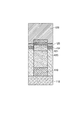
図4は、本発明の実施形態による半導体光素子110の線A−A’に沿った断面図を示している。図示された半導体光素子110は半絶縁性半導体で埋め込まれたBH構造型半導体レーザである。なお図4に示された断面図は図3の断面A−A‘での断面に限定されるものではなく、レーザ部112のどの断面も図4に示された構造を有する。
FIG. 4 is a cross-sectional view of the semiconductor
半導体光素子110は、第一導電型を有する基板118と、基板118の表面に設けられるメサ構造115と、メサ構造115を埋め込む埋め込み層122と、埋め込み層122の一部の上に設けられるパッシベーション膜123と、メサ構造115、埋め込み層122、及びパッシベーション膜123を覆うTi層124と、Ti層124上に設けられるPt層125と、Pt層125上に設けられるAu層126と、基板118の裏面に形成される第一導電型を有する電極127を有する。
The semiconductor
メサ構造115は、活性層119と、活性層119上に設けられて第一導電型とは異なる第二導電型を有するクラッド層120と、クラッド層120上に設けられて第二導電型を有するコンタクト層121を有する。Ti層124と、Pt層125と、Au層126は、第二導電型を有する電極層116を構成する。メサ構造115は、本実施形態では、図4の鉛直方向にストライプ状の共振器構造を有する。本説明では省略したが、メサ構造115にはSCH層、回折格子層等の他の層が含まれていても良い。ただしメサ構造115の最上層はコンタクト層である。また本実施形態では、基板118はn型InP基板、活性層119はInGaAsPを含む多重量子井戸、クラッド層120はp型のInP層、コンタクト層121はp型のInGaAs層とした。さらにメサ構造115共振器構造はλ/4シフト回折格子構造とした。
The
半導体光素子110はInGaAsP系材料で構成されるが他の材料系で構成されてもよい。埋め込み層122は半絶縁性半導体で構成される。ここではFeが添加されたInP層とした。コンタクト層121の上面ではTi層124、Pt層125、及びAu層126からなる電極層116はオーミック電極を構成するため、低抵抗の電気的接続が十分に保たれる。本実施形態では、第一導電型がn型で第二導電型はp型だが、実施形態によっては、第一導電型がp型で第二導電型はn型であってもよい。
The semiconductor
半導体光素子の通電及び放熱並びに後工程(ワイヤボンディング、はんだ付け)を考慮すると、Auを電極として用いることが好ましい。しかし電極層中のAuはメサ構造中の半導体層中へ拡散することで、半導体光素子の信頼性及び特性を劣化させる恐れがある。そのようなAuの半導体層への拡散を防止するため、Pt電極層がバリア層としてAu電極層の下に設けられる。コンタクト層121とAu層126は直接接触せず、Auの半導体結晶への拡散はPt層125のバリアメタル効果により抑制される。しかしPtの半導体への接着強度は弱いため、接着層及びオーミック電極を形成するため、Ti層124がPt層125と埋め込み層122及びメサ構造115上部との間に設けられる。
In consideration of energization and heat radiation of the semiconductor optical device and post-processes (wire bonding, soldering), it is preferable to use Au as an electrode. However, since Au in the electrode layer diffuses into the semiconductor layer in the mesa structure, the reliability and characteristics of the semiconductor optical device may be deteriorated. In order to prevent such diffusion of Au into the semiconductor layer, a Pt electrode layer is provided below the Au electrode layer as a barrier layer. The
前述したように、Auは通電及び放熱のためにメサ構造以外の領域に広がっていることが必要である。そのためたとえAu電極層がメサ構造へ及ぼす応力は大きいとしても、Au層が半導体層へ及ぼす応力は不可避である。しかしPt層とTi層は電極本来の機能である通電以外の目的を主として設けられている。そのためPt層とTi層はメサ構造に応力を及ぼさないことが好ましい。 As described above, Au needs to spread to a region other than the mesa structure for conduction and heat dissipation. Therefore, even if the stress applied to the mesa structure by the Au electrode layer is large, the stress applied to the semiconductor layer by the Au layer is inevitable. However, the Pt layer and the Ti layer are provided mainly for purposes other than the energization, which is the original function of the electrode. Therefore, it is preferable that the Pt layer and the Ti layer do not exert a stress on the mesa structure.
上記観点から鋭意検討した結果、本願発明者等は、Pt層とTi層がメサ構造へ及ぼす応力を緩和するため、メサ構造の側面に接するPt電極層及び/又はTi電極層と上面に接するPt電極層及び/又はTi電極層の繋がりを弱くすることに想到した。具体的には本願発明者等は、Pt電極層及び/又はTi電極層がメサ構造上部と側部で分離する半導体光素子を提案した。Pt層及び/又はTi層は、メサ構造の上部のみに形成されることが好ましいが、実際にはメサ構造の側部にもある程度形成される。 As a result of intensive studies from the above viewpoints, the present inventors have found that in order to alleviate the stress exerted by the Pt layer and the Ti layer on the mesa structure, the Pt electrode layer in contact with the side surface of the mesa structure and / or the Pt electrode layer in contact with the Ti electrode layer and the upper surface thereof The inventors have conceived of weakening the connection between the electrode layer and / or the Ti electrode layer. Specifically, the present inventors have proposed a semiconductor optical device in which a Pt electrode layer and / or a Ti electrode layer are separated at the upper part and the side part of the mesa structure. The Pt layer and / or the Ti layer are preferably formed only on the upper portion of the mesa structure, but are actually formed to some extent on the side portions of the mesa structure.
前述した半導体光素子の電極層は、メサ構造の側部で分離しているためメサ構造の上部であるコンタクト層側部への電極層による応力は緩和され、メサ構造全体の応力緩和が実現され、その結果本願実施形態による半導体光素子のSMSR歩留りを3%改善させることを本願発明者等は発見した。 Since the electrode layer of the semiconductor optical device described above is separated at the side of the mesa structure, the stress by the electrode layer on the side of the contact layer, which is the upper part of the mesa structure, is reduced, and the stress of the entire mesa structure is reduced. As a result, the present inventors have found that the SMSR yield of the semiconductor optical device according to the present embodiment is improved by 3%.
図5は、本願実施形態による半導体光素子のメサ構造の図4のBでの拡大断面図を示している。本実施形態では、コンタクト層121の全部が埋め込み層122から露出している。すなわち本実施形態では、埋め込み層122から露出するメサ構造115の上部はコンタクト層121である。本実施形態では、Ti層124及びPt層125の両者がコンタクト層121の側部において分離されて不連続となっている。また、それぞれのコンタクト層121上部に形成された領域の厚さと、埋め込み層122上部に形成された領域の厚さとは略等しい。なお実施形態によっては、コンタクト層121より下に位置する層(例えばクラッド層120)が埋め込み層122から露出してもよい。本実施形態では、Ti層124の厚さがコンタクト層121の埋め込み層122から露出した部分の厚さ(以下、Hと呼称)より薄く(Ti層<H)、また、Pt層125の厚さも露出した部分の厚さより薄い(Pt厚<H)。さらに、Ti層124とPt層125の厚さの合計は、Hよりも大きい。そのため、Pt層125の上に配置されるAu層126が露出部(半導体層であるコンタクト層121)の側部に接することがなく、Au拡散の懸念はない。なお、本実施形態ではコンタクト層121の埋め込み層122から露出した部分の厚さは200nmで、Ti層124の厚さは100nmで、Pt層125は150nmで、かつ、Au層126は1000nmである。
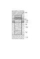
FIG. 5 is an enlarged cross-sectional view of the mesa structure of the semiconductor optical device according to the present embodiment in FIG. 4B. In the present embodiment, the
図5に示されたメサ構造においては、Ti層124は、コンタクト層121の側部において分離されて不連続となっている。そのため、連続している場合と比較して、本実施形態による半導体光素子では、メサ構造115へのTi層124が及ぼす応力は緩和される。さらに、Pt層125も同様に不連続となっており、メサ構造115へのPt層125が及ぼす応力は緩和される。
In the mesa structure shown in FIG. 5, the
[第2実施形態]
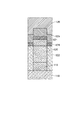
図6は、本願実施形態による半導体光素子のメサ構造の拡大断面図を示している。本実施形態では、Pt層125がメサ構造115の側壁で連続していることを除き、第1実施形態と同様である。本実施形態では、Pt層厚は250nmとした。Ti層124はメサ構造115の側壁で分離しているので、Ti層124がコンタクト層121へ及ぼす応力は緩和される。よって本実施形態でも同様の効果が得られる。
[Second embodiment]
FIG. 6 is an enlarged sectional view of the mesa structure of the semiconductor optical device according to the present embodiment. This embodiment is the same as the first embodiment except that the
[第3実施形態]
図7は、本願実施形態による半導体光素子のメサ構造の拡大断面図を示している。本実施形態では、Ti層124がメサ構造115の側壁で連続していることを除き、第1実施形態と同様である。本実施形態では、Ti層厚は250nmとした。Pt層125がメサ構造115の側壁で分離しているので、コンタクト層121へ及ぼされる応力は緩和される。よって本実施形態でも同様の効果が得られる。
[Third embodiment]
FIG. 7 is an enlarged sectional view of the mesa structure of the semiconductor optical device according to the present embodiment. This embodiment is the same as the first embodiment except that the
[第4実施形態]
図8は、本願実施形態による半導体光素子のメサ構造の拡大断面図を示している。本実施形態では、コンタクト層121の一部が埋め込み層122から露出していること、Pt層の厚さが異なる点を除き、第1実施形態と同様である。また本実施形態では、露出している部分の厚さHは150nmであり、Pt層厚は100nmとした。本実施形態においても、コンタクト層121の一部しか露出していないとしても、Ti層124とPt層125がメサ構造115の側壁で分離しているので、コンタクト層121の露出した部分へ及ぼされる応力は緩和される。よって本実施形態でも同様の効果が得られる。逆に、メサ構造のうち、クラッド層120の一部まで露出していたとしても、Ti層124及び/又はPt層125が不連続であれば、本実施形態と同様の効果が得られる。
[Fourth embodiment]
FIG. 8 is an enlarged sectional view of the mesa structure of the semiconductor optical device according to the present embodiment. This embodiment is the same as the first embodiment except that a part of the
[第5実施形態]
図9は、本願実施形態による半導体光素子のメサ構造の拡大断面図を示している。本実施形態では、Ti層124とPt層125の厚さが異なることを除いて第1実施形態と同様である。ここではTi層厚は50nm、Pt層厚は100nmとした。なお、コンタクト層121の埋め込み層122から露出した部分の厚さHは200nmである。本実施形態では、Ti層124とPt層125がメサ構造115の側壁で分離しているので、コンタクト層121の露出した部分へ及ぼされる応力は緩和される。ただし、Ti層124とPt層125の合計の厚さはHより薄いために、メサ構造の側壁にはAu層126が接している。Au層126が半導体層(コンタクト層121)に接している場合は、Auが半導体内部に拡散する恐れがあるが、その領域が小さい場合は信頼性などへの影響は小さい。そのため、本構造においても本願発明の効果は得られる。
[Fifth Embodiment]
FIG. 9 is an enlarged sectional view of the mesa structure of the semiconductor optical device according to the present embodiment. This embodiment is the same as the first embodiment except that the thicknesses of the
なお、本実施形態1乃至3と実施形態4,5は各々適宜組み合わせても良い。本願発明は、メサ構造の一部が埋め込み層より露出している状態において、Ti層及び/又はPt層が不連続でメサ上部から埋め込み層上部に配置されていることに特徴がある。 The first to third embodiments and the fourth and fifth embodiments may be appropriately combined. The present invention is characterized in that, in a state where a part of the mesa structure is exposed from the buried layer, the Ti layer and / or the Pt layer are discontinuously arranged from the upper part of the mesa to the upper part of the buried layer.
[本願実施形態による半導体光素子の製造方法]
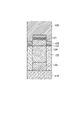
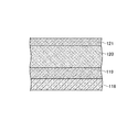
本願実施形態による半導体光素子の製造方法が図10,11,12,13示されている。最初に図10に示されているように、複数の層を含む発光に適した活性層119が基板118上に堆積され、活性層119上にクラッド層120が堆積され、p型InPクラッド層120上にコンタクト層121が堆積される。基板118はたとえばn型InP基板であってよい。活性層119はたとえば多重量子井戸であってよい。活性層119はまた、レーザの発振状態を制御する回折格子層を有してよい。コンタクト層121はたとえばp型InGaAsであってよい。
[Method of Manufacturing Semiconductor Optical Device According to Embodiment]
FIGS. 10, 11, 12, and 13 show a method of manufacturing a semiconductor optical device according to the present embodiment. First, as shown in FIG. 10, an
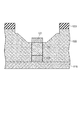
次にエッチング処理によりメサ構造115が形成され、続いて埋め込み層122を選択的に堆積することによってBH構造が形成される。たとえば埋め込み層122は半絶縁性InPであってよい。メサ構造115の幅は単一モード発振条件を満たすように決定されることが好ましい。メサ構造115の幅はたとえば約2マイクロメートル以下であってよい。埋め込み層122の結晶成長時には、メサ上部にはメサ幅より少し太い幅のマスクが配置されているために、図11に示されているように、埋め込み層122はメサ上部において少し平坦な領域があり、その後結晶面に沿って斜め上に延び、また平坦部が続く形状となる。続いて、埋め込み層122の上面にパッシベーション膜123を成膜した後、メサ構造115の幅より大きな幅でパッシベーション膜123をエッチングし、メサ構造115との電気的接続のための構造が作成される(図11)。
Next, a
その後図12に示されているように、コンタクト層121の側部が埋め込み層122から露出するようにエッチングが行なわれる。コンタクト層121は埋め込み層122から全体又は一部が露出する。
Thereafter, as shown in FIG. 12, etching is performed so that the side portions of
次に図13に示されているように、Ti層124、Pt層125、及びAu層126がこの順に堆積される。結果としてp型電極が形成される。最後に基板118の裏面にn型電極127が形成される。
Next, as shown in FIG. 13, a
以上の構造により、本発明はコンタクト層上面にTi、Pt、及びAuからなるオーミック電極による抵抗値の小さい電気的接続を有し、Ti層124及び/又はPt層125がコンタクト層側部において分離していることで、Ti層124及び/又はPt層125によるコンタクト層側部への応力が緩和される。これにより、メサ構造115に及ぼされる応力が低減される。結果として、応力に起因する屈折率変化及び回折格子ピッチの変化が低減されること等で、SMSR歩留り向上が実現される。
With the above structure, the present invention has an electrical connection with a small resistance value by an ohmic electrode made of Ti, Pt and Au on the upper surface of the contact layer, and the
本実施形態は、InGaAsP系EA−DFBレーザについて述べたが、BH構造を有するその他材料を用いた半導体レーザ、および半導体レーザ集積素子にも同様の効果が期待できる。さらに、この半導体光素子110を用いた光送信モジュール106、光送受信モジュール100においても同様の効果が得られることは言うまでもない。
Although the present embodiment has described the InGaAsP-based EA-DFB laser, a similar effect can be expected for a semiconductor laser using another material having a BH structure and a semiconductor laser integrated device. Further, it goes without saying that the same effect can be obtained in the
100 光送受信モジュール、101 筺体、102 エッジ・コネクタ、103 プリント基板、104 集積回路、105 フレキシブル基板、106 光送信モジュール、107 光受信モジュール、108a,b 光ファイバコネクタ、109 チップキャリア、110 半導体光素子、111 凸レンズ、112 レーザ部、113 導波路部、114 変調器部、115 メサ構造、116 電極、117 電極パッド、118 基板、119 活性層、120 クラッド層、121 コンタクト層、122 埋め込み層、123 パッシベーション膜、124 Ti層、125 Pt層、126 Au層、127 電極。
REFERENCE SIGNS
Claims (10)
前記基板上に設けられる活性層、該活性層上に設けられて前記第一導電型とは異なる第二導電型を有するクラッド層、及び前記クラッド層上に設けられる第二導電型を有するコンタクト層を含むメサ構造と、
前記基板上に設けられ、かつ、前記メサ構造を埋め込む埋め込み層と、
前記コンタクト層上と前記埋め込み層上に設けられる少なくとも2つの層を含む電極層、
を有し、
前記メサ構造の上部は前記埋め込み層から露出し、
前記メサ構造上と前記埋め込み層上に堆積される前記電極層のうちの一の層及び/又は該一の層上に堆積される他の層は、前記メサ構造の上部の側壁で分離する、
ことを特徴とする半導体光素子。 A substrate having a first conductivity type;
An active layer provided on the substrate, a cladding layer provided on the active layer and having a second conductivity type different from the first conductivity type, and a contact layer having a second conductivity type provided on the cladding layer And a mesa structure including
A buried layer provided on the substrate, and burying the mesa structure;
An electrode layer including at least two layers provided on the contact layer and the buried layer;
Has,
An upper portion of the mesa structure is exposed from the buried layer,
One of the electrode layers deposited on the mesa structure and the buried layer and / or another layer deposited on the one layer is separated by a top sidewall of the mesa structure;
A semiconductor optical device, comprising:
前記他の層の厚さが、前記メサ構造の上部が前記埋め込み層から露出している部分の厚さより厚く、
前記他の層は前記コンタクト層上から前記埋め込み層上において、連続的に繋がっており、
前記一の層は、前記メサ構造の上部の側壁で分離する、
ことを特徴とする半導体光素子。 The semiconductor optical device according to claim 1, wherein
The thickness of the other layer is greater than the thickness of the portion where the top of the mesa structure is exposed from the buried layer,
The other layer is continuously connected from the contact layer to the buried layer,
The one layer is separated by an upper sidewall of the mesa structure;
A semiconductor optical device, comprising:
前記一の層の厚さが、前記メサ構造の上部が前記埋め込み層から露出している部分の厚さより厚く、
前記一の層は前記コンタクト層上から前記埋め込み層上において、連続的に繋がっており、
前記他の層は、前記メサ構造の上部の側壁で分離する、
ことを特徴とする半導体光素子。 The semiconductor optical device according to claim 1, wherein
The thickness of the one layer is greater than the thickness of a portion where the upper part of the mesa structure is exposed from the buried layer,
The one layer is continuously connected on the buried layer from the contact layer,
The other layer is separated by an upper sidewall of the mesa structure;
A semiconductor optical device, comprising:
前記メサ構造の内、前記埋め込み層から露出している領域は、前記コンタクト層の一部である、
ことを特徴とする半導体光素子。 The semiconductor optical device according to claim 1, wherein
In the mesa structure, a region exposed from the buried layer is a part of the contact layer.
A semiconductor optical device, comprising:
前記一の層と前記他の層の厚さの合計は、前記メサ構造の上部が前記埋め込み層から露出している厚さより薄い、
ことを特徴とする半導体光素子。 The semiconductor optical device according to claim 1, wherein
The sum of the thicknesses of the one layer and the other layer is smaller than the thickness of the top of the mesa structure exposed from the buried layer.
A semiconductor optical device, comprising:
前記一の層と前記他の層の厚さの合計は、前記メサ構造の上部が前記埋め込み層から露出している厚さより厚い、
ことを特徴とする半導体光素子。 The semiconductor optical device according to claim 1, wherein:
The sum of the thicknesses of the one layer and the other layer is greater than the thickness of the top of the mesa structure exposed from the buried layer,
A semiconductor optical device, comprising:
前記メサ構造の内、前記埋め込み層から露出している領域は、前記コンタクト層の全部である、
ことを特徴とする半導体光素子。 The semiconductor optical device according to claim 1, wherein:
In the mesa structure, a region exposed from the buried layer is the entire contact layer.
A semiconductor optical device, comprising:
前記電極層のうちの一の層はTiであり、
前記電極層のうちの他の層はPtである、
ことを特徴とする半導体光素子。 The semiconductor optical device according to claim 1, wherein:
One of the electrode layers is Ti;
The other of the electrode layers is Pt;
A semiconductor optical device, comprising:
Priority Applications (1)
| Application Number | Priority Date | Filing Date | Title |
|---|---|---|---|
| JP2018119555A JP7112262B2 (en) | 2018-06-25 | 2018-06-25 | Semiconductor optical device and optical transmission module |
Applications Claiming Priority (1)
| Application Number | Priority Date | Filing Date | Title |
|---|---|---|---|
| JP2018119555A JP7112262B2 (en) | 2018-06-25 | 2018-06-25 | Semiconductor optical device and optical transmission module |
Publications (2)
| Publication Number | Publication Date |
|---|---|
| JP2020004754A true JP2020004754A (en) | 2020-01-09 |
| JP7112262B2 JP7112262B2 (en) | 2022-08-03 |
Family
ID=69100365
Family Applications (1)
| Application Number | Title | Priority Date | Filing Date |
|---|---|---|---|
| JP2018119555A Active JP7112262B2 (en) | 2018-06-25 | 2018-06-25 | Semiconductor optical device and optical transmission module |
Country Status (1)
| Country | Link |
|---|---|
| JP (1) | JP7112262B2 (en) |
Citations (4)
| Publication number | Priority date | Publication date | Assignee | Title |
|---|---|---|---|---|
| JPH0529708A (en) * | 1991-07-24 | 1993-02-05 | Toshiba Corp | Semiconductor laser device and manufacturing method thereof |
| JP2008277492A (en) * | 2007-04-27 | 2008-11-13 | Matsushita Electric Ind Co Ltd | Semiconductor light emitting device and manufacturing method thereof |
| JP2012019053A (en) * | 2010-07-07 | 2012-01-26 | Opnext Japan Inc | Semiconductor optical element, optical transmission module, optical transmission and reception module, and optical transmission apparatus |
| JP2012059890A (en) * | 2010-09-08 | 2012-03-22 | Nichia Chem Ind Ltd | Nitride semiconductor laser element and method of manufacturing the same |
-
2018
- 2018-06-25 JP JP2018119555A patent/JP7112262B2/en active Active
Patent Citations (4)
| Publication number | Priority date | Publication date | Assignee | Title |
|---|---|---|---|---|
| JPH0529708A (en) * | 1991-07-24 | 1993-02-05 | Toshiba Corp | Semiconductor laser device and manufacturing method thereof |
| JP2008277492A (en) * | 2007-04-27 | 2008-11-13 | Matsushita Electric Ind Co Ltd | Semiconductor light emitting device and manufacturing method thereof |
| JP2012019053A (en) * | 2010-07-07 | 2012-01-26 | Opnext Japan Inc | Semiconductor optical element, optical transmission module, optical transmission and reception module, and optical transmission apparatus |
| JP2012059890A (en) * | 2010-09-08 | 2012-03-22 | Nichia Chem Ind Ltd | Nitride semiconductor laser element and method of manufacturing the same |
Also Published As
| Publication number | Publication date |
|---|---|
| JP7112262B2 (en) | 2022-08-03 |
Similar Documents
| Publication | Publication Date | Title |
|---|---|---|
| JP5387671B2 (en) | Semiconductor laser and integrated device | |
| JP5451332B2 (en) | Optical semiconductor device | |
| JP2021193756A (en) | Optical semiconductor element, optical module, and method for manufacturing optical semiconductor element | |
| JP2009152605A (en) | Superminence diode integrated with optical amplifier and external cavity laser using the same | |
| US8488918B2 (en) | Semiconductor optical device, optical transmitter module, optical transceiver module, and optical transmission equipment | |
| JP6717733B2 (en) | Semiconductor optical integrated circuit | |
| JP2014229744A (en) | Semiconductor light-emitting assembly | |
| JP6414365B1 (en) | Semiconductor optical integrated device | |
| JP2020021865A (en) | Semiconductor optical device and optical transceiver module | |
| US12334712B2 (en) | Optical semiconductor integrated element and method of manufacturing optical semiconductor integrated element | |
| JP6220202B2 (en) | Semiconductor optical device and optical module | |
| JP4411938B2 (en) | Modulator integrated semiconductor laser, optical modulation system, and optical modulation method | |
| US20150092803A1 (en) | Laser diode and transmitter module | |
| WO2019207624A1 (en) | Semiconductor optical integrated device | |
| JP7147979B2 (en) | optical device | |
| JP6479293B1 (en) | Optical transmission device | |
| JP2018098419A (en) | Semiconductor laser, light source unit, communication system, and wavelength multiplex optical communication system | |
| JP7112262B2 (en) | Semiconductor optical device and optical transmission module | |
| JPH11186661A (en) | Semiconductor laser with modulator | |
| JP2004311556A (en) | Semiconductor laser, optical module and function integrated laser using the same | |
| JPH10275960A (en) | Optical semiconductor device | |
| JP2006203100A (en) | Semiconductor laser and light transmitter module | |
| JP2004037485A (en) | Semiconductor optical modulator and semiconductor optical device | |
| JP2013243169A (en) | Semiconductor photonic device and optical module | |
| CN102540504A (en) | Electro-absorption modulator and optical semiconductor device |
Legal Events
| Date | Code | Title | Description |
|---|---|---|---|
| A621 | Written request for application examination |
Free format text: JAPANESE INTERMEDIATE CODE: A621 Effective date: 20210602 |
|
| A977 | Report on retrieval |
Free format text: JAPANESE INTERMEDIATE CODE: A971007 Effective date: 20220322 |
|
| A131 | Notification of reasons for refusal |
Free format text: JAPANESE INTERMEDIATE CODE: A131 Effective date: 20220405 |
|
| A521 | Request for written amendment filed |
Free format text: JAPANESE INTERMEDIATE CODE: A523 Effective date: 20220602 |
|
| TRDD | Decision of grant or rejection written | ||
| A01 | Written decision to grant a patent or to grant a registration (utility model) |
Free format text: JAPANESE INTERMEDIATE CODE: A01 Effective date: 20220705 |
|
| A61 | First payment of annual fees (during grant procedure) |
Free format text: JAPANESE INTERMEDIATE CODE: A61 Effective date: 20220722 |
|
| R150 | Certificate of patent or registration of utility model |
Ref document number: 7112262 Country of ref document: JP Free format text: JAPANESE INTERMEDIATE CODE: R150 |
|
| R250 | Receipt of annual fees |
Free format text: JAPANESE INTERMEDIATE CODE: R250 |