JP2020004806A - Semiconductor device and method of mounting semiconductor chip - Google Patents
Semiconductor device and method of mounting semiconductor chip Download PDFInfo
- Publication number
- JP2020004806A JP2020004806A JP2018121381A JP2018121381A JP2020004806A JP 2020004806 A JP2020004806 A JP 2020004806A JP 2018121381 A JP2018121381 A JP 2018121381A JP 2018121381 A JP2018121381 A JP 2018121381A JP 2020004806 A JP2020004806 A JP 2020004806A
- Authority
- JP
- Japan
- Prior art keywords
- metal layer
- semiconductor chip
- solder
- semiconductor
- mounting
- Prior art date
- Legal status (The legal status is an assumption and is not a legal conclusion. Google has not performed a legal analysis and makes no representation as to the accuracy of the status listed.)
- Granted
Links
Images





Classifications
-
- H—ELECTRICITY
- H10—SEMICONDUCTOR DEVICES; ELECTRIC SOLID-STATE DEVICES NOT OTHERWISE PROVIDED FOR
- H10W—GENERIC PACKAGES, INTERCONNECTIONS, CONNECTORS OR OTHER CONSTRUCTIONAL DETAILS OF DEVICES COVERED BY CLASS H10
- H10W72/00—Interconnections or connectors in packages
- H10W72/90—Bond pads, in general
-
- H—ELECTRICITY
- H10—SEMICONDUCTOR DEVICES; ELECTRIC SOLID-STATE DEVICES NOT OTHERWISE PROVIDED FOR
- H10W—GENERIC PACKAGES, INTERCONNECTIONS, CONNECTORS OR OTHER CONSTRUCTIONAL DETAILS OF DEVICES COVERED BY CLASS H10
- H10W70/00—Package substrates; Interposers; Redistribution layers [RDL]
- H10W70/20—Conductive package substrates serving as an interconnection, e.g. metal plates
- H10W70/24—Conductive package substrates serving as an interconnection, e.g. metal plates characterised by materials
-
- H—ELECTRICITY
- H10—SEMICONDUCTOR DEVICES; ELECTRIC SOLID-STATE DEVICES NOT OTHERWISE PROVIDED FOR
- H10W—GENERIC PACKAGES, INTERCONNECTIONS, CONNECTORS OR OTHER CONSTRUCTIONAL DETAILS OF DEVICES COVERED BY CLASS H10
- H10W20/00—Interconnections in chips, wafers or substrates
- H10W20/40—Interconnections external to wafers or substrates, e.g. back-end-of-line [BEOL] metallisations or vias connecting to gate electrodes
-
- H—ELECTRICITY
- H10—SEMICONDUCTOR DEVICES; ELECTRIC SOLID-STATE DEVICES NOT OTHERWISE PROVIDED FOR
- H10W—GENERIC PACKAGES, INTERCONNECTIONS, CONNECTORS OR OTHER CONSTRUCTIONAL DETAILS OF DEVICES COVERED BY CLASS H10
- H10W40/00—Arrangements for thermal protection or thermal control
- H10W40/10—Arrangements for heating
-
- H—ELECTRICITY
- H10—SEMICONDUCTOR DEVICES; ELECTRIC SOLID-STATE DEVICES NOT OTHERWISE PROVIDED FOR
- H10W—GENERIC PACKAGES, INTERCONNECTIONS, CONNECTORS OR OTHER CONSTRUCTIONAL DETAILS OF DEVICES COVERED BY CLASS H10
- H10W70/00—Package substrates; Interposers; Redistribution layers [RDL]
- H10W70/60—Insulating or insulated package substrates; Interposers; Redistribution layers
-
- H—ELECTRICITY
- H10—SEMICONDUCTOR DEVICES; ELECTRIC SOLID-STATE DEVICES NOT OTHERWISE PROVIDED FOR
- H10W—GENERIC PACKAGES, INTERCONNECTIONS, CONNECTORS OR OTHER CONSTRUCTIONAL DETAILS OF DEVICES COVERED BY CLASS H10
- H10W74/00—Encapsulations, e.g. protective coatings
-
- H—ELECTRICITY
- H10—SEMICONDUCTOR DEVICES; ELECTRIC SOLID-STATE DEVICES NOT OTHERWISE PROVIDED FOR
- H10W—GENERIC PACKAGES, INTERCONNECTIONS, CONNECTORS OR OTHER CONSTRUCTIONAL DETAILS OF DEVICES COVERED BY CLASS H10
- H10W74/00—Encapsulations, e.g. protective coatings
- H10W74/01—Manufacture or treatment
- H10W74/014—Manufacture or treatment using batch processing
-
- H—ELECTRICITY
- H10—SEMICONDUCTOR DEVICES; ELECTRIC SOLID-STATE DEVICES NOT OTHERWISE PROVIDED FOR
- H10W—GENERIC PACKAGES, INTERCONNECTIONS, CONNECTORS OR OTHER CONSTRUCTIONAL DETAILS OF DEVICES COVERED BY CLASS H10
- H10W95/00—Packaging processes not covered by the other groups of this subclass
-
- H—ELECTRICITY
- H10—SEMICONDUCTOR DEVICES; ELECTRIC SOLID-STATE DEVICES NOT OTHERWISE PROVIDED FOR
- H10W—GENERIC PACKAGES, INTERCONNECTIONS, CONNECTORS OR OTHER CONSTRUCTIONAL DETAILS OF DEVICES COVERED BY CLASS H10
- H10W72/00—Interconnections or connectors in packages
- H10W72/071—Connecting or disconnecting
- H10W72/072—Connecting or disconnecting of bump connectors
- H10W72/07231—Techniques
- H10W72/07236—Soldering or alloying
-
- H—ELECTRICITY
- H10—SEMICONDUCTOR DEVICES; ELECTRIC SOLID-STATE DEVICES NOT OTHERWISE PROVIDED FOR
- H10W—GENERIC PACKAGES, INTERCONNECTIONS, CONNECTORS OR OTHER CONSTRUCTIONAL DETAILS OF DEVICES COVERED BY CLASS H10
- H10W72/00—Interconnections or connectors in packages
- H10W72/071—Connecting or disconnecting
- H10W72/073—Connecting or disconnecting of die-attach connectors
- H10W72/07331—Connecting techniques
- H10W72/07336—Soldering or alloying
-
- H—ELECTRICITY
- H10—SEMICONDUCTOR DEVICES; ELECTRIC SOLID-STATE DEVICES NOT OTHERWISE PROVIDED FOR
- H10W—GENERIC PACKAGES, INTERCONNECTIONS, CONNECTORS OR OTHER CONSTRUCTIONAL DETAILS OF DEVICES COVERED BY CLASS H10
- H10W72/00—Interconnections or connectors in packages
- H10W72/071—Connecting or disconnecting
- H10W72/073—Connecting or disconnecting of die-attach connectors
- H10W72/07351—Connecting or disconnecting of die-attach connectors characterised by changes in properties of the die-attach connectors during connecting
- H10W72/07353—Connecting or disconnecting of die-attach connectors characterised by changes in properties of the die-attach connectors during connecting changes in shapes
-
- H—ELECTRICITY
- H10—SEMICONDUCTOR DEVICES; ELECTRIC SOLID-STATE DEVICES NOT OTHERWISE PROVIDED FOR
- H10W—GENERIC PACKAGES, INTERCONNECTIONS, CONNECTORS OR OTHER CONSTRUCTIONAL DETAILS OF DEVICES COVERED BY CLASS H10
- H10W72/00—Interconnections or connectors in packages
- H10W72/20—Bump connectors, e.g. solder bumps or copper pillars; Dummy bumps; Thermal bumps
-
- H—ELECTRICITY
- H10—SEMICONDUCTOR DEVICES; ELECTRIC SOLID-STATE DEVICES NOT OTHERWISE PROVIDED FOR
- H10W—GENERIC PACKAGES, INTERCONNECTIONS, CONNECTORS OR OTHER CONSTRUCTIONAL DETAILS OF DEVICES COVERED BY CLASS H10
- H10W72/00—Interconnections or connectors in packages
- H10W72/30—Die-attach connectors
-
- H—ELECTRICITY
- H10—SEMICONDUCTOR DEVICES; ELECTRIC SOLID-STATE DEVICES NOT OTHERWISE PROVIDED FOR
- H10W—GENERIC PACKAGES, INTERCONNECTIONS, CONNECTORS OR OTHER CONSTRUCTIONAL DETAILS OF DEVICES COVERED BY CLASS H10
- H10W72/00—Interconnections or connectors in packages
- H10W72/30—Die-attach connectors
- H10W72/331—Shapes of die-attach connectors
- H10W72/334—Cross-sectional shape, i.e. in side view
-
- H—ELECTRICITY
- H10—SEMICONDUCTOR DEVICES; ELECTRIC SOLID-STATE DEVICES NOT OTHERWISE PROVIDED FOR
- H10W—GENERIC PACKAGES, INTERCONNECTIONS, CONNECTORS OR OTHER CONSTRUCTIONAL DETAILS OF DEVICES COVERED BY CLASS H10
- H10W72/00—Interconnections or connectors in packages
- H10W72/30—Die-attach connectors
- H10W72/351—Materials of die-attach connectors
- H10W72/352—Materials of die-attach connectors comprising metals or metalloids, e.g. solders
-
- H—ELECTRICITY
- H10—SEMICONDUCTOR DEVICES; ELECTRIC SOLID-STATE DEVICES NOT OTHERWISE PROVIDED FOR
- H10W—GENERIC PACKAGES, INTERCONNECTIONS, CONNECTORS OR OTHER CONSTRUCTIONAL DETAILS OF DEVICES COVERED BY CLASS H10
- H10W72/00—Interconnections or connectors in packages
- H10W72/90—Bond pads, in general
- H10W72/921—Structures or relative sizes of bond pads
- H10W72/923—Bond pads having multiple stacked layers
-
- H—ELECTRICITY
- H10—SEMICONDUCTOR DEVICES; ELECTRIC SOLID-STATE DEVICES NOT OTHERWISE PROVIDED FOR
- H10W—GENERIC PACKAGES, INTERCONNECTIONS, CONNECTORS OR OTHER CONSTRUCTIONAL DETAILS OF DEVICES COVERED BY CLASS H10
- H10W72/00—Interconnections or connectors in packages
- H10W72/90—Bond pads, in general
- H10W72/931—Shapes of bond pads
-
- H—ELECTRICITY
- H10—SEMICONDUCTOR DEVICES; ELECTRIC SOLID-STATE DEVICES NOT OTHERWISE PROVIDED FOR
- H10W—GENERIC PACKAGES, INTERCONNECTIONS, CONNECTORS OR OTHER CONSTRUCTIONAL DETAILS OF DEVICES COVERED BY CLASS H10
- H10W72/00—Interconnections or connectors in packages
- H10W72/90—Bond pads, in general
- H10W72/951—Materials of bond pads
- H10W72/952—Materials of bond pads comprising metals or metalloids, e.g. PbSn, Ag or Cu
Landscapes
- Die Bonding (AREA)
Abstract
【課題】半導体チップに形成した発熱素子の領域の裏面側において、半田内に生じる気泡の発生を減少させた半導体装置、および、半導体チップの搭載方法を提供する【解決手段】半導体装置は、搭載基板100と搭載基板100上にAuSn半田90を介して搭載された半導体チップ1とを備える。半導体チップ1は、搭載基板100に対向する裏面に形成されたAuからなる裏面金属層60と、表面側に形成した発熱素子を有し、発熱素子を形成した領域を除く裏面に、AuSn半田と濡れ性の悪いNiCr、Ni、Tiのいずれか1つからなる半田阻止金属層70が半導体チップ1の縁まで延びて露出している。半導体チップ1を搭載基板100上でスクラブすることによって、AuSn半田90に生じた気泡が半田阻止金属層70にできた間隙Cを通じて半導体チップの外部に排出される。【選択図】図1CThe present invention provides a semiconductor device in which the generation of bubbles generated in solder is reduced on the back side of a region of a heating element formed on a semiconductor chip, and a method of mounting a semiconductor chip. The semiconductor device includes a substrate 100 and a semiconductor chip 1 mounted on the mounting substrate 100 via AuSn solder 90. The semiconductor chip 1 has a back metal layer 60 made of Au formed on the back surface facing the mounting substrate 100, and a heating element formed on the front surface side. AuSn solder is applied to the back surface excluding the region where the heating element is formed. The solder blocking metal layer 70 made of any one of NiCr, Ni, and Ti having poor wettability extends to the edge of the semiconductor chip 1 and is exposed. By scrubbing the semiconductor chip 1 on the mounting substrate 100, bubbles generated in the AuSn solder 90 are discharged to the outside of the semiconductor chip through the gap C formed in the solder blocking metal layer 70. [Selection] Fig. 1C
Description
本発明は半導体装置、および、半導体チップの搭載方法に関する。 The present invention relates to a semiconductor device and a method for mounting a semiconductor chip.
一般的に、フェイスアップで実装されるMMIC(Monolithic Microwave Integrated Circuit)は、銀(Ag)ペーストや金錫(AuSn)半田によってパッケージに固定される。AuSn半田を用いる際は、半導体チップとパッケージとの間に介在するAuSn半田を溶かし、半導体チップ裏面に形成した金(Au)とパッケージ表面に形成したAuを固定する。AuSn半田は熱伝導率が悪いため、薄ければ薄いほどよい。また、気泡(ボイド)が入ると半導体チップからパッケージへの熱抵抗が著しく大きくなる。そのためAuSn半田を用いた実装では半導体チップを揺さぶること(スクラブ)でAuSn半田を薄く形成し、かつ、気泡が入らないように実装している。 Generally, an MMIC (Monolithic Microwave Integrated Circuit) mounted face-up is fixed to a package with silver (Ag) paste or gold tin (AuSn) solder. When using the AuSn solder, the AuSn solder interposed between the semiconductor chip and the package is melted, and gold (Au) formed on the back surface of the semiconductor chip and Au formed on the package surface are fixed. Since AuSn solder has poor thermal conductivity, the thinner the better, the better. In addition, when air bubbles (voids) enter, the thermal resistance from the semiconductor chip to the package increases significantly. Therefore, in the mounting using AuSn solder, the semiconductor chip is shaken (scrubbed) to form the AuSn solder thinly and to prevent bubbles from entering.
しかしながら、従来、スクラブを行っても、製造時のバラツキによって気泡を完全に無くすことは難しかった。半導体チップに形成したFET(Field effect transistor:電界効果トランジスタ)部分の下部に気泡があると、FETの発熱による温度上昇が想定よりも大きくなり、デバイスの寿命を低下させていた。 However, conventionally, even when scrubbing is performed, it has been difficult to completely eliminate bubbles due to variations during manufacturing. If air bubbles are present below a field effect transistor (FET) portion formed on a semiconductor chip, the temperature rise due to the heat generated by the FET becomes larger than expected, thereby shortening the life of the device.
半導体チップの実装時に、気泡による悪影響を防ぐために、例えば、特許文献1には、減圧炉を用いて溶融半田中の気泡を除去することが開示されている。また、特許文献2には、半導体チップ裏面のFETの活性領域と重ならない箇所に溝を設け、ダイボンド時のスクラブによって、AuSn半田内に生ずる気泡を溝内に捕集させることが開示されている。
For example,
しかしながら、特許文献1に開示された方法では、真空引きにより気泡を追い出しているため、真空排気装置が必要となる。また、特許文献2に開示された方法では、スクラブ時にAuSn半田が溝内に入り込み、気泡の捕集ができなくなるといった問題があった。
However, in the method disclosed in
本発明は、これらの実情に鑑みてなされたものであり、半導体チップに形成した発熱素子の領域の裏面側において、半田内に生じる気泡の発生を減少させた半導体装置、および、半導体チップの搭載方法を提供することを目的とする。 The present invention has been made in view of these circumstances, and has a semiconductor device in which the generation of bubbles generated in solder is reduced on the back surface side of a region of a heating element formed on a semiconductor chip, and a mounting method of the semiconductor chip. The aim is to provide a method.
本発明の一態様に係る半導体装置は、搭載基板と該搭載基板上にAuSn半田を介して搭載された半導体チップとを備え、該半導体チップは、前記搭載基板に対向する裏面側に形成されたAuからなる裏面金属層と、表面側に形成した発熱素子を有し、該発熱素子を形成した領域を除く前記裏面側で、NiCr、Ni、Tiのいずれか1つからなる半田阻止金属層が前記半導体チップの縁まで延びて露出している。 A semiconductor device according to one embodiment of the present invention includes a mounting substrate and a semiconductor chip mounted on the mounting substrate via AuSn solder, and the semiconductor chip is formed on a back surface side facing the mounting substrate. A backside metal layer made of Au and a heating element formed on the front side, and a solder blocking metal layer made of any one of NiCr, Ni, and Ti on the backside except for a region where the heating element is formed, The semiconductor chip extends to the edge of the semiconductor chip and is exposed.
また、本発明の一態様に係る半導体チップの搭載方法は、半導体発熱素子を含む第1の領域と、前記半導体発熱素子を含まない第2の領域を有する半導体チップを搭載基板上にAuSn半田を介して搭載する半導体チップの搭載方法であって、前記半導体チップの裏面にシード金属層を形成する工程と、該シード金属層の上にAuからなる裏面金属層を形成する工程と、該裏面金属層の前記第2の領域内において、NiCr、Ni、Tiのいずれか1つからなり前記半導体チップの縁まで延びる半田阻止金属層を形成する工程と、前記裏面金属層を前記AuSn半田に接触させ、前記半導体チップを前記搭載基板上でスクラブする工程と、を有する。 In addition, the method for mounting a semiconductor chip according to one embodiment of the present invention is a method of mounting a semiconductor chip having a first region including a semiconductor heating element and a second region not including the semiconductor heating element on a mounting substrate using AuSn solder. A method of mounting a seed metal layer on the back surface of the semiconductor chip, a step of forming a back metal layer made of Au on the seed metal layer, Forming a solder blocking metal layer made of any one of NiCr, Ni and Ti in the second region of the layer and extending to the edge of the semiconductor chip; contacting the back metal layer with the AuSn solder; Scrubbing the semiconductor chip on the mounting substrate.
さらに、本発明の一態様に係る半導体チップの搭載方法は、半導体発熱素子を含む第1の領域と、前記半導体発熱素子を含まない第2の領域を有する半導体チップを搭載基板上にAuSn半田を介して搭載する半導体チップの搭載方法であって、前記半導体チップの裏面にNiCr、Ni、Tiのいずれか1つからなる半田阻止金属層を形成する工程と、 該半田阻止金属層の上にAuからなる裏面金属層を形成する工程と、該裏面金属層の前記第2の領域内において、前記半田阻止金属層を前記半導体チップの縁に至るまで露出させる工程と、前記裏面金属層を前記AuSn半田に接触させ、前記半導体チップを前記搭載基板上でスクラブする工程と、を有する。 Further, in the method for mounting a semiconductor chip according to one embodiment of the present invention, a semiconductor chip having a first region including a semiconductor heating element and a second region not including the semiconductor heating element may be formed using AuSn solder on a mounting substrate. A method of mounting a semiconductor chip to be mounted via a semiconductor chip, comprising: forming a solder blocking metal layer made of any one of NiCr, Ni, and Ti on the back surface of the semiconductor chip; Forming a back metal layer comprising: a step of exposing the solder blocking metal layer to an edge of the semiconductor chip in the second region of the back metal layer; and forming the back metal layer by AuSn. Contacting with solder to scrub the semiconductor chip on the mounting substrate.
本発明によれば、半導体チップに形成した発熱素子の領域の裏面側において、半田内に生じる気泡の発生を減少させることができる。 ADVANTAGE OF THE INVENTION According to this invention, the generation | occurrence | production of the bubble generate | occur | produced in solder can be reduced on the back surface side of the area | region of the heating element formed in the semiconductor chip.
(本願発明の実施形態の説明)
最初に本願発明の実施態様を列記して説明する。
(1)本発明の一態様に係る半導体装置は、搭載基板と該搭載基板上にAuSn半田を介して搭載された半導体チップとを備え、該半導体チップは、前記搭載基板に対向する裏面側に形成されたAuからなる裏面金属層と、表面側に形成した発熱素子を有し、該発熱素子を形成した領域を除く前記裏面側で、NiCr、Ni、Tiのいずれか1つからなる半田阻止金属層が前記半導体チップの縁まで延びて露出している。
この構成により、AuSn半田に発生したボイドを、AuSn半田と濡れ性の悪い半田阻止金属層の周りに収集し、外部へ排除することが可能となる。これにより、半導体チップに形成した発熱素子の領域の裏面側において、AuSn半田内に生じる気泡の発生を減少させることができ、半導体チップのからの熱を効率よく放熱することができる。
(Description of the embodiment of the present invention)
First, embodiments of the present invention will be listed and described.
(1) A semiconductor device according to one embodiment of the present invention includes a mounting substrate and a semiconductor chip mounted on the mounting substrate via AuSn solder, and the semiconductor chip is provided on a back surface side facing the mounting substrate. A backside metal layer made of Au formed and a heating element formed on the front side, and solder blocking made of any one of NiCr, Ni, and Ti on the backside except for a region where the heating element is formed. A metal layer extends to the edge of the semiconductor chip and is exposed.
With this configuration, voids generated in the AuSn solder can be collected around the solder blocking metal layer having poor wettability with the AuSn solder, and can be removed to the outside. Thereby, on the back surface side of the region of the heating element formed on the semiconductor chip, the generation of bubbles generated in the AuSn solder can be reduced, and the heat from the semiconductor chip can be efficiently radiated.
(2)前記裏面金属層が、前記半導体チップの前記裏面側に形成したシード金属層の上に形成されていてもよい。
この構成により、裏面金属を選択電解メッキによって形成することができ、裏面電極の厚さの調整が容易になる。
(2) The back surface metal layer may be formed on a seed metal layer formed on the back surface side of the semiconductor chip.
With this configuration, the back metal can be formed by selective electrolytic plating, and the thickness of the back electrode can be easily adjusted.
(3)前記半田阻止金属層が、前記裏面金属層の上に形成されていることが望ましい。
この構成により、半田阻止金属層が裏面電極層の上に凸状に形成されるため、半田に生じた気泡の収集効率が高めることができる。
(3) Preferably, the solder blocking metal layer is formed on the back metal layer.
With this configuration, the solder blocking metal layer is formed in a convex shape on the back electrode layer, so that the efficiency of collecting bubbles generated in the solder can be increased.
(4)前記シード金属層が、NiCr、Ni、Tiのいずれか1つからなる半田阻止金属層として形成され、該半田阻止金属層が前記裏面金属層の除去部分で露出してもよい。
この構成により、シード金属層を半田阻止金属層として兼用できるため、半導体チップの裏面に形成した金属層の総数を減少させることができる。
(4) The seed metal layer may be formed as a solder blocking metal layer made of any one of NiCr, Ni, and Ti, and the solder blocking metal layer may be exposed at a portion where the back metal layer is removed.
With this configuration, the seed metal layer can also be used as a solder blocking metal layer, so that the total number of metal layers formed on the back surface of the semiconductor chip can be reduced.
(5)前記半田阻止金属層が、前記半導体チップの一の縁から、該一の縁と対向する他の縁にまで直線状に露出していることが望ましい。
この構成により、半田阻止金属層の周りに収集した気泡を、半導体チップの外部へ排除させやすくなる。
(5) It is preferable that the solder blocking metal layer is linearly exposed from one edge of the semiconductor chip to another edge facing the one edge.
With this configuration, bubbles collected around the solder blocking metal layer can be easily removed to the outside of the semiconductor chip.
(6)前記搭載基板は、前記半導体チップを収納するパッケージの底材であってよい。
この構成により、パッケージの底材に半導体チップを搭載した際に、半導体チップからの熱がパッケージの底材を通じて効率よく放熱する。
(6) The mounting substrate may be a bottom material of a package that houses the semiconductor chip.
With this configuration, when the semiconductor chip is mounted on the bottom material of the package, heat from the semiconductor chip is efficiently radiated through the bottom material of the package.
(7)本発明の一態様に係る半導体チップの搭載方法は、半導体発熱素子を含む第1の領域と、前記半導体発熱素子を含まない第2の領域を有する半導体チップを搭載基板上にAuSn半田を介して搭載する半導体チップの搭載方法であって、前記半導体チップの裏面にシード金属層を形成する工程と、該シード金属層の上にAuからなる裏面金属層を形成する工程と、該裏面金属層の前記第2の領域内において、NiCr、Ni、Tiのいずれか1つからなり前記半導体チップの縁まで延びる半田阻止金属層を形成する工程と、前記裏面金属層を前記AuSn半田に接触させ、前記半導体チップを前記搭載基板上でスクラブする工程と、を有する。
この構成により、AuSn半田に発生したボイドを、AuSn半田と濡れ性の悪い半田阻止金属層の周りに収集し、外部へ排除することが可能となる。このため、半導体チップに形成した発熱素子の領域の裏面側において、半田内に生じる気泡の発生を減少させることができ、半導体チップのからの熱を効率よく放熱することができる。また、半田阻止金属層が裏面電極層の上に突出して形成されるため、半田に生じた気泡の収集効率が高めることができる。
(7) A method for mounting a semiconductor chip according to one embodiment of the present invention is a method of mounting a semiconductor chip having a first region including a semiconductor heating element and a second region not including the semiconductor heating element on a mounting substrate using AuSn solder. Forming a seed metal layer on a back surface of the semiconductor chip, forming a back metal layer made of Au on the seed metal layer, Forming a solder blocking metal layer made of any one of NiCr, Ni, and Ti extending to an edge of the semiconductor chip in the second region of the metal layer, and contacting the back metal layer with the AuSn solder; And scrubbing the semiconductor chip on the mounting substrate.
With this configuration, voids generated in the AuSn solder can be collected around the solder blocking metal layer having poor wettability with the AuSn solder, and can be removed to the outside. Therefore, on the back surface side of the region of the heating element formed on the semiconductor chip, the generation of bubbles generated in the solder can be reduced, and the heat from the semiconductor chip can be efficiently radiated. Further, since the solder blocking metal layer is formed so as to protrude above the back electrode layer, the efficiency of collecting bubbles generated in the solder can be increased.
(8)また、本発明の一態様に係る半導体チップの搭載方法は、半導体発熱素子を含む第1の領域と、前記半導体発熱素子を含まない第2の領域を有する半導体チップを搭載基板上にAuSn半田を介して搭載する半導体チップの搭載方法であって、前記半導体チップの裏面にNiCr、Ni、Tiのいずれか1つからなる半田阻止金属層を形成する工程と、 該半田阻止金属層の上にAuからなる裏面金属層を形成する工程と、該裏面金属層の前記第2の領域内において、前記半田阻止金属層を前記半導体チップの縁に至るまで露出させる工程と、前記裏面金属層を前記AuSn半田に接触させ、前記半導体チップを前記搭載基板上でスクラブする工程と、を有する。
この構成により、AuSn半田に発生したボイドを、AuSn半田と濡れ性の悪い半田阻止金属層の周りに収集し、外部へ排除することが可能となる。このため、半導体チップに形成した発熱素子の領域の裏面側において、半田内に生じる気泡の発生を減少させることができ、半導体チップのからの熱を効率よく放熱することができる。
(8) In addition, in the method for mounting a semiconductor chip according to one embodiment of the present invention, a semiconductor chip having a first region including a semiconductor heating element and a second region not including the semiconductor heating element is mounted on a mounting substrate. A method of mounting a semiconductor chip to be mounted via AuSn solder, comprising: forming a solder blocking metal layer made of any one of NiCr, Ni, and Ti on a back surface of the semiconductor chip; Forming a backside metal layer made of Au thereon, exposing the solder blocking metal layer to the edge of the semiconductor chip in the second region of the backside metal layer; In contact with the AuSn solder to scrub the semiconductor chip on the mounting substrate.
With this configuration, voids generated in the AuSn solder can be collected around the solder blocking metal layer having poor wettability with the AuSn solder, and can be removed to the outside. Therefore, on the back surface side of the region of the heating element formed on the semiconductor chip, the generation of bubbles generated in the solder can be reduced, and the heat from the semiconductor chip can be efficiently radiated.
(本願発明の実施形態の詳細)
以下、図面を参照しながら、本発明の半導体装置、および、半導体チップの搭載方法に係る好適な実施形態について説明する。以下の説明において、異なる図面においても同じ符号を付した構成は同様のものであるとして、その説明を省略する場合がある。なお、本発明はこれらの実施形態での例示に限定されるものではなく、特許請求の範囲に記載された事項の範囲内および均等の範囲内におけるすべての変更を含む。また、複数の実施形態について組み合わせが可能である限り、本発明は任意の実施形態を組み合わせたものを含む。
(Details of the embodiment of the present invention)
Hereinafter, preferred embodiments of a semiconductor device and a semiconductor chip mounting method of the present invention will be described with reference to the drawings. In the following description, configurations denoted by the same reference numerals in different drawings are similar, and description thereof may be omitted. It should be noted that the present invention is not limited to the exemplifications of these embodiments, and includes all changes within the scope of the matters described in the claims and within the equivalent scope. In addition, the present invention includes a combination of any of the embodiments as long as a combination of a plurality of embodiments is possible.
(第1の実施形態)
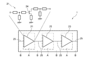
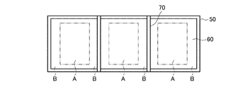
図1Aは、本発明の一実施形態に係る半導体装置の半導体チップの表面を模式的に示す図であり、図1Bは、図1Aに示す半導体チップの裏面を示す図である。また、図1Cは、本発明の一実施形態に係る半導体装置の断面を示す図であり、図1A、図1Bに示す半導体チップを搭載基板上に搭載した際の断面を示している。以下の説明では、半導体チップとして,MMICを例に説明するが、半導体チップとしてはこれに限られない。
(1st Embodiment)
FIG. 1A is a diagram schematically illustrating a front surface of a semiconductor chip of a semiconductor device according to an embodiment of the present invention, and FIG. 1B is a diagram illustrating a back surface of the semiconductor chip illustrated in FIG. 1A. FIG. 1C is a diagram showing a cross section of the semiconductor device according to one embodiment of the present invention, and shows a cross section when the semiconductor chip shown in FIGS. 1A and 1B is mounted on a mounting substrate. In the following description, an MMIC will be described as an example of a semiconductor chip, but the semiconductor chip is not limited to this.
MMICは、1つ以上の高周波回路ブロックを1つの半導体基板上に設けた集積回路であり、能動素子と受動素子とが半導体製造プロセスによって、一体に形成されている。図1Aに示す半導体チップ1の例では、約1mm×約3mmのSiC(シリコンカーバイト)基板10上に形成したGaAs(砒化ガリウム)エピタキシャル層20に、初段アンプ21、中段アンプ22、および、終段アンプ23の多段のアンプを形成した例を示している。各アンプ21〜23は、それぞれ能動素子であるFET24と受動素子から構成されており、伝送線路25によって接続されている。
An MMIC is an integrated circuit in which one or more high-frequency circuit blocks are provided on one semiconductor substrate, and an active element and a passive element are integrally formed by a semiconductor manufacturing process. In the example of the
半導体チップ1は、動作時において、FET24が発熱素子となるため、FET24を備えた各アンプ21〜23の箇所で最も発熱量が多くなり、伝送線路25のみが施された個所では発熱量が小さい。図1Aでは、発熱素子を含む領域をAで示し、発熱素子を含まない領域をBで示している。発熱素子を含まない領域Bは半導体チップの周辺部と各アンプ21〜23の段間の領域になる。そして、半導体チップ1の裏面をAuSn半田90によって搭載基板100上にマウントした際に、領域Aに気泡が生じると、発熱素子であるFET24からの熱が効率よく放熱されないため、領域Aの温度が高くなり、回路特性が劣化し、半導体装置の寿命が低下する。
During operation, the
半導体チップ1の裏面には、シード金属層50と、このシード金属層50の上にAuからなる裏面金属層60がメッキされている。そして、本実施形態では、裏面金属層60の上に、AuSn半田90と濡れ性の悪いニッケルクロム(NiCr)、ニッケル(Ni)、チタン(Ti)のいずれか1つからなる金属層70が設けられている。図1Bに示すように、この金属層70は半導体チップ1の一つの縁から半導体チップ1の裏面側の段間の領域を通って、この一つの縁と反対の縁まで延びている。このように、金属層70は、半導体チップ1の裏面から見た場合、裏面金属層60の上で露出している。
On the back surface of the
半導体チップ1は、搭載基板100の上にAuSn半田90を用いて搭載される。搭載基板100は、半導体チップ1を収納するパッケージの底材であり、例えば、銅(Cu)から構成されるが、他の材料であってもよい。半導体チップ1の搭載時に、NiCr、Ni、TiはAuSn半田90と濡れ性に劣るためAuSn半田を弾く。このため、金属層70の周囲には、図1Cに示すように空隙Cが生じる。そして、半導体チップ1の搭載時に搭載基板100上でスクラブ(擦り合わせ)を行うことによって、AuSn半田90に生じた気泡は空隙Cに収集され、半導体チップ1の縁まで形成されたこの空隙Cに沿って外部に排出される。
The
これによって、領域Aに対応する裏面金属層60上に発生する気泡を減少させることができる。また、領域Bでは空隙Cが生じるため、裏面金属層60から搭載基板100への熱伝達が悪化し、領域Bの温度が上昇するが、この領域BにはFET等の発熱素子を設けていないため、半導体チップ1の寿命を短くさせることがない。
Thereby, bubbles generated on the
(半導体チップの搭載方法)
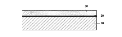
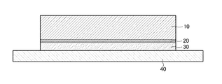
次に、半導体チップの搭載方法について説明する。図2A〜図2Jは、本発明の一実施形態に係る半導体チップの搭載方法における各工程を説明するための図である。図2Aは表面プロセス工程、図2Bはフォトレジスト塗布工程、図2Cは支持基板貼付工程、図2Dは裏面研磨工程、図2Eはシード金属層形成工程、図2Fは裏面金属層メッキ工程、図2Gは半田阻止金属層形成工程、図2Hは半田阻止金属層パターニング工程、図2Iはエキスパンディングテープ貼付工程、図2Jはダイシング工程をそれぞれ示しており、各工程が順次行われる。なお、図2A〜図2Jにおいて、各構成部材の厚さの関係は、目視し易くするために実際の厚さの関係と異ならせている。また、図1Cは、ダイボンディング工程を説明するために用いられる。
(Method of mounting semiconductor chip)
Next, a method for mounting a semiconductor chip will be described. 2A to 2J are views for explaining each step in the method for mounting a semiconductor chip according to one embodiment of the present invention. 2A is a surface processing step, FIG. 2B is a photoresist coating step, FIG. 2C is a supporting substrate attaching step, FIG. 2D is a backside polishing step, FIG. 2E is a seed metal layer forming step, FIG. 2F is a backside metal layer plating step, and FIG. 2H shows a solder blocking metal layer forming step, FIG. 2H shows a solder blocking metal layer patterning step, FIG. 2I shows an expanding tape attaching step, and FIG. 2J shows a dicing step, and each step is sequentially performed. In FIGS. 2A to 2J, the relationship of the thickness of each component is different from the relationship of the actual thickness to make it easy to see. FIG. 1C is used to explain a die bonding step.
(表面プロセス工程)
表面プロセス工程では、図2Aに示すように、厚さ500μm程度の半導体基板10の表面上にGaA等のエピタキシャル層20を形成し、このエピタキシャル層20に、能動素子、およびエピタキシャル層20上に絶縁層を介して受動素子、伝送線路などを形成し、MMICを構成する複数の半導体チップ1を形成する。これらの素子は、既存の半導体製造技術を用いて作製される。例えば、図1Aに示すように、多段のアンプ21〜23とこれらのアンプ21〜23を接続する伝送線路25が形成される。
(Surface processing step)
In the surface process step, as shown in FIG. 2A, an
(フォトレジスト塗布工程)
次に、図2Bに示すように、基板10の表面側に形成した各素子を保護するために、基板の表面側(エピタキシャル層20側)にフォトレジスト30を塗布し、さらに、フォトレジスト30の上にワックス(図示しない)を塗布する。
(Photoresist coating process)
Next, as shown in FIG. 2B, in order to protect each element formed on the front side of the
(支持基板貼付工程)
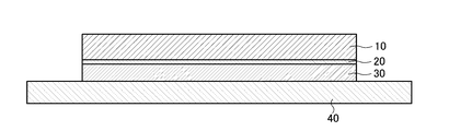
次に、基板10の裏面側(エピタキシャル層20の反対面側)の処理のために、図2Cに示すように、表面側(エピタキシャル層20側)をガラス製の支持基板40に対向させて貼り付ける。
(Support substrate sticking process)
Next, as shown in FIG. 2C, for the treatment on the back side of the substrate 10 (the side opposite to the epitaxial layer 20), the
(裏面研磨工程)
次に、図2Dに示すように、基板10が所定の厚さとなるように裏面をグラインダで研磨する。基板10の厚さは、表面に形成した信号線用の金属パターンと裏面金属層60とが基板10を介してマイクロストリップ線路を形成する際に、線路の特性インピーダンスを所望の値にするために調整される。なお、表面側のグランド電位の金属パターンと裏面金属層60とは図示しないビアホールを介して電気的に接続される。本工程で、基板10は例えば100μm程度の厚さに研磨される。
(Backside polishing process)
Next, as shown in FIG. 2D, the back surface is polished with a grinder so that the
(シード金属層形成工程)
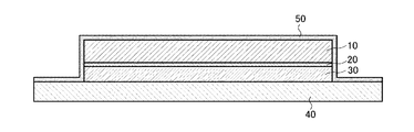
次に、図2Eに示すように、シード金属層50として、NiCrとAuの2層からなるシード金属層50をSiC基板10の裏面に全面スパッタリングによって形成する。このシード金属層50は、後工程で裏面金属層60を選択電解メッキで形成するために用いられる。シード金属層50のNiCrとAuは、それぞれ、例えば200nmと2000nmの厚さで形成される。
(Seed metal layer forming step)
Next, as shown in FIG. 2E, a
(背面金属層メッキ工程)
基板10には、図2Fに示すように、所定幅D1を有するスクライブラインで区画され複数の半導体チップが形成されている。シード金属層50を形成した後、シード金属層50の全面にフォトレジストを設け、半導体チップの領域を残して、スクライブライン間の幅D1を覆うフォトレジスト61によってパターニングする。そして、半導体チップの裏面に露出したシード金属層50上に、Auからなる裏面金属層60を例えば10μmの厚さで選択電解メッキにより形成する。フォトレジスト61は裏面金属層60の形成後に除去する。
(Back metal layer plating process)
As shown in FIG. 2F, a plurality of semiconductor chips partitioned by scribe lines having a predetermined width D1 are formed on the
(半田阻止金属層形成工程)
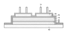
次に、図2Gに示すように、フォトレジスト61を除去した後、AuSn半田と濡れ性の悪い、例えば、NiCrを裏面金属層60の全面にスパッタリングよって形成し、厚さ50nm程度の金属層70を設ける。その後、金属層70上に、フォトレジスト71をパターニングする。
(Solder blocking metal layer forming step)
Next, as shown in FIG. 2G, after the
(半田阻止金属層パターニング工程)
次に、フォトレジスト71をマスクとして金属層70をエッチングし、図2Hに示すように、裏面金属層60の上に幅100μm程度のライン状の金属層70を残す。この金属層70は、図1Bに示すように、半導体チップ1の領域Bに半導体チップ1の縁から他方の縁まで延びている。この工程は、図2Gに示すように、NiCrからなる金属層70を残す領域をフォトレジスト71でマスクし、金属層70をウェットエッチンし、その後、フォトレジスト71を除去することによって行われる。
(Solder blocking metal layer patterning process)
Next, the
(エキスパンディングテープ貼付工程)
次に、図2Iに示すように、基板10の裏面側をエキスパンディングテープ80に貼り付けた後、表面側のワックス(図示なし)とフォトレジスト30を除去し、基板を支持基板40から外す。なお、表面側のワックス(図示なし)とフォトレジスト30を除去して、基板10を支持基板40から外した後、基板10の裏面側をエキスパンディングテープ80に貼り付けてもよい。この工程では、基板10はダイシング前であるので、各半導体チップ1は分離することがない。
(Expanding tape attaching process)
Next, as shown in FIG. 2I, after attaching the back surface of the
(ダイシング工程)
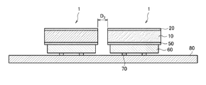
次に、図2Jに示すように、基板10の表面側からダイシングにより、半導体チップ1を分離する。ダイシングは、スクライブラインに沿って、例えば、スクライブラインの幅D1内で、スクライブラインの幅D1よりも狭い幅D2を有するダイシングブレードを用いて行う。そして、各半導体チップ1をエキスパンディングテープ80から外し、個々の半導体チップ1を得る。
(Dicing process)
Next, as shown in FIG. 2J, the
(ダイボンディング工程)
次に、図1Cに示すように、個々の半導体チップ1を、例えば配線基板、あるいは、パッケージの底材(金属製)からなる搭載基板100上にダイボンディングする。ダイボンディングは、搭載基板100上に予めAuSn半田90をボール状あるいはシート状(薄膜状)に設けておき、例えば、320°Cの窒素ガス(N2)雰囲気中でAuSn半田90を搭載基板100の上で溶かし、搭載基板100上で半導体チップ1をスクラブする(擦り合わせる)ことにより行う。
(Die bonding process)
Next, as shown in FIG. 1C, the
その際、先述したように、NiCrからなる金属層70は、AuSn半田90に対し濡れ性に劣るため、実装時に金属層70の部分には空隙Cができる。AuSn半田に生じた気泡がスクラブによって金属層70に達すれば、気泡はライン状の金属層70に沿ってチップ外に抜けていく。また、溶解したAuSn半田90はAuと濡れ性が良いため、半導体チップ1の裏面金属層60のAuと搭載基板100側のAuの間で一様な厚さに広がる。この時のAuSn半田の厚さは10μm程度になる。これにより、半導体チップ1の領域Aの裏面側には気泡がなくなるため、発熱効率が高まり、回路特性の劣化を抑え、半導体装置の長寿命を図ることができる。
At this time, as described above, since the
(第2の実施形態)
本発明では、裏面金属層60と搭載基板100とをAuSn半田90を用いて固着する際に、AuSn半田90に生じる気泡を、AuSn半田90と濡れ性の悪い金属層70のパターンによって収集し、半導体チップ1の外部へ排出できるようにしている。このため、金属層70のパターンは、半導体チップ1の裏面から見た際に、裏面金属層60から露出していればよい。第1の実施形態では、基板10の裏面側にシード金属層50と裏面金属層60を順番に設け、裏面金属層60の上に金属層70をパターニングすることにより、金属層70を露出させている。
(Second embodiment)
In the present invention, when the
第2の実施形態では、シード金属層50の材料を、AuSn半田90と濡れ性の悪いNiCr、Ni、Tiのいずれか1つからなる材料で構成し、シード金属層50に半田阻止金属層の機能を持たせている。このため、第2の実施形態では、シード金属層50が金属層70となる。そして、このシード金属層50の上に形成した裏面金属層60を一部除去することによって、シード金属層50を露出させる。シード金属層50が露出する領域は、半導体チップ1の領域B内で、また、半導体チップ1の縁まで延びている。裏面金属層60から露出したシード金属層50の金属層70に対応する機能は、第1の実施形態と同様であるので、その説明を省略する。
In the second embodiment, the material of the
以上、本発明の実施形態に係る半導体装置、および、半導体チップの搭載方法について説明したが、AuSn半田90と濡れ性の悪い金属層70のパターンは、ライン状のものに限られず、格子状のものあるいはその他の形状であってもよい。
As described above, the semiconductor device according to the embodiment of the present invention and the method of mounting the semiconductor chip have been described. However, the pattern of the
1…半導体チップ、
10…基板、
20…エピタキシャル層、
21…初段アンプ、
22…中段アンプ、
23…終段アンプ、
24…FET、
25…伝送線路、
30…フォトレジスト、
40…支持基板、
50…シード金属層、
60…裏面金属層、
61…フォトレジスト、
70…半田阻止金属層、
71…フォトレジスト、
80…エキスパンディングテープ、
90…AuSn半田、
100…搭載基板。
1 ... Semiconductor chip,
10 ... substrate,
20 ... Epitaxial layer,
21 ... First stage amplifier,
22 ... middle stage amplifier,
23 ... final stage amplifier,
24 ... FET,
25 ... transmission line,
30 ... photoresist,
40 ... support substrate,
50: seed metal layer,
60 ... back metal layer,
61 ... photoresist,
70 ... Solder blocking metal layer,
71 ... photoresist,
80 ... Expanding tape,
90 ... AuSn solder,
100 mounting board.
Claims (8)
該半導体チップは、前記搭載基板に対向する裏面側に形成されたAuからなる裏面金属層と、表面側に形成した発熱素子を有し、
該発熱素子を形成した領域を除く前記裏面側で、NiCr、Ni、Tiのいずれか1つからなる半田阻止金属層が前記半導体チップの縁まで延びて露出している、
半導体装置。 A mounting substrate and a semiconductor chip mounted on the mounting substrate via AuSn solder;
The semiconductor chip has a back metal layer made of Au formed on the back surface facing the mounting substrate, and a heating element formed on the front surface,
On the rear surface side excluding the region where the heating element is formed, a solder blocking metal layer made of any one of NiCr, Ni, and Ti extends to the edge of the semiconductor chip and is exposed.
Semiconductor device.
前記半導体チップの裏面にシード金属層を形成する工程と、
該シード金属層の上にAuからなる裏面金属層を形成する工程と、
該裏面金属層の前記第2の領域内において、NiCr、Ni、Tiのいずれか1つからなり前記半導体チップの縁まで延びる半田阻止金属層を形成する工程と、
前記裏面金属層を前記AuSn半田に接触させ、前記半導体チップを前記搭載基板上でスクラブする工程と、を有する半導体チップの搭載方法。 A semiconductor chip mounting method for mounting a semiconductor chip having a first region including a semiconductor heating element and a second region not including the semiconductor heating element on a mounting substrate via AuSn solder,
Forming a seed metal layer on the back surface of the semiconductor chip;
Forming a back metal layer made of Au on the seed metal layer;
Forming a solder blocking metal layer made of any one of NiCr, Ni and Ti and extending to an edge of the semiconductor chip in the second region of the back metal layer;
Contacting the backside metal layer with the AuSn solder and scrubbing the semiconductor chip on the mounting substrate.
前記半導体チップの裏面にNiCr、Ni、Tiのいずれか1つからなる半田阻止金属層を形成する工程と、
該半田阻止金属層の上にAuからなる裏面金属層を形成する工程と、
該裏面金属層の前記第2の領域内において、前記半田阻止金属層を前記半導体チップの縁に至るまで露出させる工程と、
前記裏面金属層を前記AuSn半田に接触させ、前記半導体チップを前記搭載基板上でスクラブする工程と、を有する半導体チップの搭載方法。 A semiconductor chip mounting method for mounting a semiconductor chip having a first region including a semiconductor heating element and a second region not including the semiconductor heating element on a mounting substrate via AuSn solder,
Forming a solder blocking metal layer made of any one of NiCr, Ni, and Ti on the back surface of the semiconductor chip;
Forming a backside metal layer made of Au on the solder blocking metal layer;
Exposing the solder blocking metal layer to the edge of the semiconductor chip in the second region of the back metal layer;
Contacting the backside metal layer with the AuSn solder and scrubbing the semiconductor chip on the mounting substrate.
Priority Applications (4)
| Application Number | Priority Date | Filing Date | Title |
|---|---|---|---|
| JP2018121381A JP7168280B2 (en) | 2018-06-26 | 2018-06-26 | Semiconductor device and semiconductor chip mounting method |
| CN201910547770.0A CN110648978A (en) | 2018-06-26 | 2019-06-24 | Semiconductor device and method of manufacturing the same |
| US16/450,644 US11031365B2 (en) | 2018-06-26 | 2019-06-24 | Semiconductor device having a solder blocking metal layer |
| US17/240,045 US20210242162A1 (en) | 2018-06-26 | 2021-04-26 | Method of manufacturing semiconductor device |
Applications Claiming Priority (1)
| Application Number | Priority Date | Filing Date | Title |
|---|---|---|---|
| JP2018121381A JP7168280B2 (en) | 2018-06-26 | 2018-06-26 | Semiconductor device and semiconductor chip mounting method |
Publications (2)
| Publication Number | Publication Date |
|---|---|
| JP2020004806A true JP2020004806A (en) | 2020-01-09 |
| JP7168280B2 JP7168280B2 (en) | 2022-11-09 |
Family
ID=68980936
Family Applications (1)
| Application Number | Title | Priority Date | Filing Date |
|---|---|---|---|
| JP2018121381A Active JP7168280B2 (en) | 2018-06-26 | 2018-06-26 | Semiconductor device and semiconductor chip mounting method |
Country Status (3)
| Country | Link |
|---|---|
| US (2) | US11031365B2 (en) |
| JP (1) | JP7168280B2 (en) |
| CN (1) | CN110648978A (en) |
Families Citing this family (1)
| Publication number | Priority date | Publication date | Assignee | Title |
|---|---|---|---|---|
| JP7392632B2 (en) * | 2020-11-06 | 2023-12-06 | 三菱電機株式会社 | Semiconductor device, die pad, and semiconductor device manufacturing method |
Citations (4)
| Publication number | Priority date | Publication date | Assignee | Title |
|---|---|---|---|---|
| JPS5034170A (en) * | 1973-07-27 | 1975-04-02 | ||
| JPH10223808A (en) * | 1997-02-07 | 1998-08-21 | Nec Corp | Semiconductor device |
| JP2006261551A (en) * | 2005-03-18 | 2006-09-28 | Toyota Motor Corp | Semiconductor module and manufacturing method thereof |
| JP2006351926A (en) * | 2005-06-17 | 2006-12-28 | Auto Network Gijutsu Kenkyusho:Kk | Circuit boards, electronic components and electrical junction boxes |
Family Cites Families (31)
| Publication number | Priority date | Publication date | Assignee | Title |
|---|---|---|---|---|
| JPS63312613A (en) * | 1987-06-15 | 1988-12-21 | Nec Corp | Single plate capacitor |
| DE69426090T2 (en) * | 1993-04-27 | 2001-03-01 | Nec Corp., Tokio/Tokyo | Method of manufacturing an optical semiconductor device |
| JP3461632B2 (en) * | 1995-08-28 | 2003-10-27 | 三菱電機株式会社 | Semiconductor laser device |
| DE19536463C2 (en) * | 1995-09-29 | 2002-02-07 | Infineon Technologies Ag | Method of manufacturing a plurality of laser diode devices |
| EP0793269B1 (en) * | 1996-02-28 | 2002-05-15 | Koninklijke Philips Electronics N.V. | Semiconductor device having a chip with via hole soldered on a support, and its method of fabrication |
| US6342442B1 (en) * | 1998-11-20 | 2002-01-29 | Agere Systems Guardian Corp. | Kinetically controlled solder bonding |
| JP3689637B2 (en) * | 2000-12-25 | 2005-08-31 | シャープ株式会社 | Semiconductor device and manufacturing method thereof |
| JP3882712B2 (en) * | 2002-08-09 | 2007-02-21 | 住友電気工業株式会社 | Submount and semiconductor device |
| US7247514B2 (en) * | 2003-04-11 | 2007-07-24 | Matsushita Electric Industrial Co., Ltd. | Semiconductor device and method for producing the same |
| KR100975521B1 (en) * | 2003-10-04 | 2010-08-12 | 삼성전자주식회사 | Light emitting device assembly |
| JP3994980B2 (en) * | 2004-03-29 | 2007-10-24 | 株式会社日立製作所 | Device mounting substrate, manufacturing method thereof, and semiconductor device mounting method |
| US7462861B2 (en) * | 2004-04-28 | 2008-12-09 | Cree, Inc. | LED bonding structures and methods of fabricating LED bonding structures |
| US7864398B2 (en) * | 2004-06-08 | 2011-01-04 | Gentex Corporation | Electro-optical element including metallic films and methods for applying the same |
| TWI514522B (en) * | 2005-03-18 | 2015-12-21 | 同和電子科技有限公司 | Sub-mounting sheet and manufacturing method thereof |
| JP5214844B2 (en) * | 2005-03-29 | 2013-06-19 | 日本オクラロ株式会社 | Optical semiconductor device |
| US7339267B2 (en) * | 2005-05-26 | 2008-03-04 | Freescale Semiconductor, Inc. | Semiconductor package and method for forming the same |
| US7348212B2 (en) * | 2005-09-13 | 2008-03-25 | Philips Lumileds Lighting Company Llc | Interconnects for semiconductor light emitting devices |
| US7626275B2 (en) * | 2005-12-16 | 2009-12-01 | Mitsubishi Electric Corporation | Semiconductor device |
| JP2007227464A (en) * | 2006-02-21 | 2007-09-06 | Sanyo Electric Co Ltd | Semiconductor device and manufacturing method of semiconductor device |
| JP2007294899A (en) * | 2006-03-31 | 2007-11-08 | Dowa Electronics Materials Co Ltd | Solder layer, electronic device bonding substrate using the same, and electronic device bonding submount |
| JP2008091768A (en) * | 2006-10-04 | 2008-04-17 | Sharp Corp | Semiconductor laser device and electronic equipment |
| JP2013125768A (en) * | 2011-12-13 | 2013-06-24 | Japan Oclaro Inc | Solder bonding device and reception module |
| US8970010B2 (en) * | 2013-03-15 | 2015-03-03 | Cree, Inc. | Wafer-level die attach metallization |
| PT3040390T (en) * | 2013-08-29 | 2019-09-05 | Mitsui Chemicals Tohcello Inc | ADHESIVE FILM AND METHOD FOR MANUFACTURING A SEMICONDUCTORY DEVICE |
| JP6365919B2 (en) | 2013-09-27 | 2018-08-01 | 富士電機株式会社 | Manufacturing method of semiconductor device |
| JP6305127B2 (en) * | 2014-03-12 | 2018-04-04 | 三菱電機株式会社 | Semiconductor laser light source |
| JP6544354B2 (en) * | 2014-06-27 | 2019-07-17 | ソニー株式会社 | Semiconductor device manufacturing method |
| DE102016117826B4 (en) * | 2016-09-21 | 2023-10-19 | Infineon Technologies Ag | ELECTRONIC MODULE AND PRODUCTION METHOD THEREOF |
| JP6512231B2 (en) * | 2017-01-27 | 2019-05-15 | トヨタ自動車株式会社 | Semiconductor device |
| JP6901196B2 (en) * | 2017-05-09 | 2021-07-14 | 住友電工デバイス・イノベーション株式会社 | Semiconductor module and manufacturing method of semiconductor module |
| JP6355092B1 (en) * | 2017-05-11 | 2018-07-11 | パナソニックIpマネジメント株式会社 | Solder alloy and joint structure using the same |
-
2018
- 2018-06-26 JP JP2018121381A patent/JP7168280B2/en active Active
-
2019
- 2019-06-24 CN CN201910547770.0A patent/CN110648978A/en active Pending
- 2019-06-24 US US16/450,644 patent/US11031365B2/en active Active
-
2021
- 2021-04-26 US US17/240,045 patent/US20210242162A1/en not_active Abandoned
Patent Citations (4)
| Publication number | Priority date | Publication date | Assignee | Title |
|---|---|---|---|---|
| JPS5034170A (en) * | 1973-07-27 | 1975-04-02 | ||
| JPH10223808A (en) * | 1997-02-07 | 1998-08-21 | Nec Corp | Semiconductor device |
| JP2006261551A (en) * | 2005-03-18 | 2006-09-28 | Toyota Motor Corp | Semiconductor module and manufacturing method thereof |
| JP2006351926A (en) * | 2005-06-17 | 2006-12-28 | Auto Network Gijutsu Kenkyusho:Kk | Circuit boards, electronic components and electrical junction boxes |
Also Published As
| Publication number | Publication date |
|---|---|
| US11031365B2 (en) | 2021-06-08 |
| CN110648978A (en) | 2020-01-03 |
| US20210242162A1 (en) | 2021-08-05 |
| JP7168280B2 (en) | 2022-11-09 |
| US20190393182A1 (en) | 2019-12-26 |
Similar Documents
| Publication | Publication Date | Title |
|---|---|---|
| US5770468A (en) | Process for mounting a semiconductor chip to a chip carrier by exposing a solder layer to a reducing atmosphere | |
| US6759599B2 (en) | Circuit board, method for manufacturing same, and high-output module | |
| JP2006339611A (en) | Metal-ceramic composite substrate and manufacturing method thereof | |
| US20030070292A1 (en) | Circuit board, method for manufacturing same, and high-output module | |
| JP3350152B2 (en) | Semiconductor device and method of manufacturing the same | |
| JP2006261569A (en) | Submount and manufacturing method thereof | |
| JP2009505393A (en) | AC light emitting device | |
| US20030006500A1 (en) | Circuit board, method for manufacturing same, and high-output module | |
| JP2020004806A (en) | Semiconductor device and method of mounting semiconductor chip | |
| JP2017005073A (en) | Manufacturing method of electronic device | |
| JP7332130B2 (en) | Semiconductor device manufacturing method, semiconductor device manufacturing method, semiconductor device, and semiconductor device | |
| JP5280611B2 (en) | Semiconductor device manufacturing method and device obtained | |
| JPH11238870A (en) | Semiconductor device and manufacture thereof | |
| JPH09266215A (en) | High frequency and high power semiconductor device and manufacturing method thereof | |
| JP2697683B2 (en) | Semiconductor device and manufacturing method thereof | |
| JPH07176760A (en) | Wafer having phs structure and its manufacture | |
| JP2758888B2 (en) | Semiconductor device | |
| JP2001176761A (en) | Thin-layer substrate semiconductor device and manufacturing method therefor | |
| KR100708604B1 (en) | Flip chip light emitting device using low melting metal bump and manufacturing method thereof | |
| JPH0870069A (en) | Semiconductor device | |
| JP2822506B2 (en) | Method for manufacturing semiconductor device | |
| JPH06120370A (en) | Laminated board manufacturing method | |
| JP2002231731A (en) | Method for fabricating compound semiconductor device | |
| JP2000049256A (en) | Semiconductor device structure and manufacturing method | |
| JPH0951058A (en) | SEMICONDUCTOR DEVICE, SEMICONDUCTOR DEVICE MANUFACTURING METHOD, AND MANUFACTURING DEVICE |
Legal Events
| Date | Code | Title | Description |
|---|---|---|---|
| A625 | Written request for application examination (by other person) |
Free format text: JAPANESE INTERMEDIATE CODE: A625 Effective date: 20210322 |
|
| A977 | Report on retrieval |
Free format text: JAPANESE INTERMEDIATE CODE: A971007 Effective date: 20220228 |
|
| A131 | Notification of reasons for refusal |
Free format text: JAPANESE INTERMEDIATE CODE: A131 Effective date: 20220322 |
|
| A521 | Request for written amendment filed |
Free format text: JAPANESE INTERMEDIATE CODE: A523 Effective date: 20220520 |
|
| TRDD | Decision of grant or rejection written | ||
| A01 | Written decision to grant a patent or to grant a registration (utility model) |
Free format text: JAPANESE INTERMEDIATE CODE: A01 Effective date: 20220927 |
|
| A61 | First payment of annual fees (during grant procedure) |
Free format text: JAPANESE INTERMEDIATE CODE: A61 Effective date: 20221021 |
|
| R150 | Certificate of patent or registration of utility model |
Ref document number: 7168280 Country of ref document: JP Free format text: JAPANESE INTERMEDIATE CODE: R150 |
|
| R250 | Receipt of annual fees |
Free format text: JAPANESE INTERMEDIATE CODE: R250 |