JP2020004874A - Electronic component with lead wire - Google Patents
Electronic component with lead wire Download PDFInfo
- Publication number
- JP2020004874A JP2020004874A JP2018123706A JP2018123706A JP2020004874A JP 2020004874 A JP2020004874 A JP 2020004874A JP 2018123706 A JP2018123706 A JP 2018123706A JP 2018123706 A JP2018123706 A JP 2018123706A JP 2020004874 A JP2020004874 A JP 2020004874A
- Authority
- JP
- Japan
- Prior art keywords
- lead wire
- circuit board
- sealing body
- case
- electronic component
- Prior art date
- Legal status (The legal status is an assumption and is not a legal conclusion. Google has not performed a legal analysis and makes no representation as to the accuracy of the status listed.)
- Granted
Links
Images

Landscapes
- Details Of Resistors (AREA)
- Adjustable Resistors (AREA)
Abstract
【課題】回路基板とリード線間の接続を、容易に接続不良や劣化なく確実に行うことができるリード線付き電子部品を提供すること。【解決手段】回路基板10と、回路基板10を収納するケース30と、回路基板10の接続パターン23に端子80を介して接続されるリード線50とを具備するリード線付き電子部品1である。リード線50を半田60によって端子80に接続した接続部分Aを、ケース30の材質と異なる材質からなる封止体70によって封止する。封止体70は、溶融時に接着性を有する成形材料によって構成される。【選択図】図3PROBLEM TO BE SOLVED: To provide an electronic component with a lead wire which can be easily and surely connected between a circuit board and a lead wire without a connection failure or deterioration. SOLUTION: This is an electronic component 1 with a lead wire including a circuit board 10, a case 30 for accommodating the circuit board 10, and a lead wire 50 connected to a connection pattern 23 of the circuit board 10 via a terminal 80. .. The connection portion A in which the lead wire 50 is connected to the terminal 80 by the solder 60 is sealed by a sealing body 70 made of a material different from the material of the case 30. The sealant 70 is made of a molding material that has adhesiveness when melted. [Selection diagram] Fig. 3
Description
本発明は、リード線付き電子部品に関するものである。 The present invention relates to an electronic component with a lead wire.
従来、回転式電子部品の中には、例えば特許文献1の図1に示すように、回転式電子部品用の成型品(30)の外周側壁から外方に向けて金属端子板(20)を突出する構造のものがある。この種の回転式電子部品は、例えばこれを別途用意した主回路基板上に載置し、その際、各金属端子板(20)を、前記主回路基板に形成した端子接続パターンに半田付けなどして使用される。 2. Description of the Related Art Conventionally, among rotary electronic components, as shown in FIG. 1 of Patent Document 1, for example, a metal terminal plate (20) is directed outward from an outer peripheral side wall of a molded product (30) for a rotary electronic component. Some have a protruding structure. This type of rotary electronic component is placed on a separately prepared main circuit board, for example, and each metal terminal plate (20) is soldered to a terminal connection pattern formed on the main circuit board. Used as
一方、従来、上記回転式電子部品の別の使用方法として、前記金属端子板(20)を、別途用意した主回路基板ではなく、リード線に接続して使用する場合がある。このような場合は、各金属端子板(20)に、それぞれリード線を半田付けする。 On the other hand, conventionally, as another method of using the rotary electronic component, there is a case where the metal terminal plate (20) is used by connecting to a lead wire instead of a separately prepared main circuit board. In such a case, a lead wire is soldered to each metal terminal plate (20).
しかしながら、各金属端子板(20)に、それぞれリード線を半田付けする場合は、以下のような課題があった。
即ち、金属端子板(20)とリード線との接続部分は一般に露出しているが、この接続部分には、リード線が屈曲した場合などにストレスが集中して加わり易く、このためこの接続部分に劣化や接続不良などを生じる虞があった。
However, when a lead wire is soldered to each metal terminal plate (20), there are the following problems.
That is, although the connecting portion between the metal terminal plate (20) and the lead wire is generally exposed, stress is easily concentrated on the connecting portion when the lead wire is bent. There is a possibility that deterioration or poor connection may occur.
またこの露出した接続部分は、各種液体、粉塵などによる影響を受け易く、この点からもこの接続部分に劣化や接続不良などを生じる虞があった。 In addition, the exposed connection portion is easily affected by various liquids, dusts, and the like, and from this point, there is a possibility that the connection portion may be deteriorated or poorly connected.
本発明は上述の点に鑑みてなされたものでありその目的は、端子を介して接続される回路基板とリード線間の接続を、容易に接続不良や劣化なく確実に行うことができるリード線付き電子部品を提供することにある。 The present invention has been made in view of the above points, and an object of the present invention is to provide a lead wire capable of easily and reliably connecting between a circuit board and a lead wire connected via terminals without connection failure or deterioration. Provided is an electronic component with the same.
本発明は、回路パターン及び当該回路パターンに接続される接続パターンを形成してなる回路基板と、前記回路基板を収納するケースと、前記回路基板の接続パターンに端子を介して接続されるリード線と、を具備するリード線付き電子部品において、前記リード線を前記端子に接続した接続部分を、前記ケースの材質と異なる材質からなる封止体によって封止することを特徴としている。
本発明によれば、端子とリード線間の接続部分を、封止体によって封止するので、当該接続部分を補強でき、リード線が屈曲するなどして当該接続部分にストレスが加わっても、当該接続部分の接続不良を防止することができる。同時に、封止体によって封止するので、防水、防塵を図ることができ、このことからも当該接続部分の劣化や接続不良を防止することができる。
また、封止体とケースをそれぞれ異なる材質で構成したので、ケースは回路基板を収納するのに好適な材料を、また封止体は接続部分を封止するのに好適な材料を、それぞれ選択でき、当該接続部分の接続状態を好適に維持できる。
The present invention relates to a circuit board on which a circuit pattern and a connection pattern connected to the circuit pattern are formed, a case for housing the circuit board, and a lead wire connected to the connection pattern of the circuit board via a terminal. And a connection part connecting the lead wire to the terminal is sealed with a sealing body made of a material different from a material of the case.
According to the present invention, the connection portion between the terminal and the lead wire is sealed by the sealing body, so that the connection portion can be reinforced, and even if stress is applied to the connection portion by bending the lead wire, The connection failure of the connection portion can be prevented. At the same time, sealing is performed by the sealing body, so that waterproofing and dustproofing can be achieved. This also prevents deterioration and poor connection of the connection portion.
In addition, since the sealing body and the case are made of different materials, the case selects a material suitable for housing the circuit board, and the sealing body selects a material suitable for sealing the connection portion. The connection state of the connection portion can be suitably maintained.
また本発明は、上記特徴に加え、前記リード線は、前記回路基板の接続パターンに接続した端子の前記ケースから外方に突出した部分に接続されており、前記封止体は、当該接続部分を封止していることを特徴としている。
なお、封止体は、前記接続部分からケースの端子を突出する面に接着する位置まで形成することが好ましい。ケースの面に封止体を接着しておけば、リード線が屈曲等した際に、そのストレスをケースと封止体が受け、接続部分へのストレスをより効果的に減少させることができる。
In addition, in the present invention, in addition to the above features, the lead wire is connected to a portion of the terminal connected to the connection pattern of the circuit board, the portion protruding outward from the case, and the sealing body is connected to the connection portion. Is sealed.
Preferably, the sealing body is formed up to a position where the sealing body is bonded to a surface of the case from which the terminal protrudes. If the sealing body is bonded to the surface of the case, when the lead wire is bent or the like, the stress is received by the case and the sealing body, and the stress on the connection portion can be more effectively reduced.
また本発明は、上記特徴に加え、前記封止体は、溶融時に接着性を有する成形材料によって構成されていることを特徴としている。
本発明によれば、回路基板とリード線間の接続部分に対する封止体の密着性を高くすることができるので、より効果的な防水、防塵を図ることができる。
Further, the present invention is characterized in that, in addition to the above features, the sealing body is made of a molding material having an adhesive property when melted.
ADVANTAGE OF THE INVENTION According to this invention, since the adhesiveness of the sealing body with respect to the connection part between a circuit board and a lead wire can be improved, more effective waterproofing and dust proofing can be achieved.
本発明によれば、端子を介して接続される回路基板とリード線間の接続を、容易に、接続不良や劣化なく確実に行うことができる。 ADVANTAGE OF THE INVENTION According to this invention, connection between the circuit board connected via a terminal and a lead wire can be performed easily easily, without connection failure or deterioration.
以下、本発明の実施形態を、図面を参照して詳細に説明する。
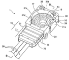
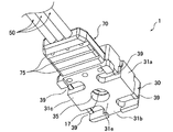
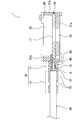
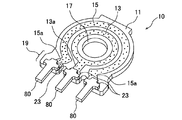
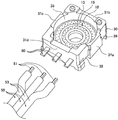
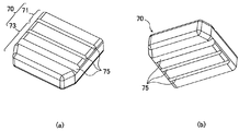
図1は本発明の一実施形態に係るリード線付き電子部品1を上側から見た斜視図、図2はリード線付き電子部品1を下側から見た斜視図、図3は図1のB−B断面概略図、図4〜図6はリード線付き電子部品1の組立方法説明図、図7は封止体70を単体で示す図である。
Hereinafter, embodiments of the present invention will be described in detail with reference to the drawings.
FIG. 1 is a perspective view of an electronic component with leads 1 according to an embodiment of the present invention as viewed from above, FIG. 2 is a perspective view of the electronic component with leads 1 viewed from below, and FIG. 4 to 6 are explanatory diagrams of an assembling method of the electronic component 1 with lead wires, and FIG. 7 is a diagram showing the
図1〜図3に示すように、リード線付き電子部品1は、回路基板10と、回路基板10を収納するケース30と、回路基板10に接続される複数本(この例では3本)の端子80と、各端子80に接続される複数本(この例では3本)のリード線50と、リード線50を端子80に接続した接続部分Aを封止し、且つ各リード線50を束ねる封止体70とを具備して構成されている。なお以下の説明において、「上」とは回路基板10の下記する回路パターン(集電パターン13や抵抗体パターン15など)を形成した面をその反対面側から見る方向いい、「下」とはその反対方向をいうものとする。
As shown in FIGS. 1 to 3, the electronic component 1 with lead wires includes a
回路基板10は、図4に示すように、硬質で絶縁性の基板(以下「硬質基板」という)11の上面に、同心円状に、集電パターン(回路パターン)13と、抵抗体パターン(回路パターン)15とを形成して構成されている。硬質基板11の略中央部分には、図示しない摺動子を取り付けた回転体を回転自在に軸支する円形の貫通孔からなる軸支孔17が設けられている。また、硬質基板11の外周辺の一部は、これを矩形状に外方に突出させることで接続パターン形成部19が形成されている。
As shown in FIG. 4, the
集電パターン13は、抵抗値の低い導電ペーストをスクリーン印刷することなどによって、前記軸支孔17の周囲を囲むようにリング状に形成されている。集電パターン13の外周からは、半径方向外方(接続パターン形成部19の方向)に向けて1本の引出パターン(回路パターン)13aが引き出され、その先端には接続パターン23が形成されている。この接続パターン23は、前記接続パターン形成部19の中央に位置している。
The
抵抗体パターン15は、所望の抵抗値を有する抵抗体ペーストをスクリーン印刷することなどによって、前記集電パターン13の周囲を囲むようにC字状に形成されている。抵抗体パターン15の両端からは、それぞれ半径方向外方(接続パターン形成部19の方向)に向けて一対の引出パターン(回路パターン)15aが引き出され、それらの先端には接続パターン23が形成されている。各接続パターン23は、それぞれ前記接続パターン形成部19の左右両側位置近傍に位置している。なお各引出パターン13a,15aと各接続パターン23は、何れも抵抗値の低い導電ペーストのスクリーン印刷によって形成されている。
The
ケース30は、図5に示すように、硬質の合成樹脂からなる一体成型品であり、上面が開放された略箱型に形成されている。即ち、ケース30は、前記回路基板10の周囲を囲む側壁31a,b,c,dと、回路基板10の底面を覆う底面部31eとを具備して構成されている。ケース30の上面中央は略円形の回転体収納部33となっている。回転体収納部33の底面には、前記回路基板10上面の集電パターン13と抵抗体パターン15が露出している。また、回路基板10の各接続パターン23には、金属板製の端子80が導電性接着剤などを用いて接続され、接続された部分の上下を、成形したケース30(その側壁31dの部分)によって挟持し、また端子80の先端側の部分をケース30の側壁31dから外部に突出している。また、ケース30の底面部31eの中央には、前記回路基板10の軸支孔17に連通する円形の貫通孔35が形成されている。さらに、ケース30の左右両側壁31a,31cから底面にかけては、ケース30の上面を覆う図示しないカバーの係止爪を挿入する溝部39が形成されている。
As shown in FIG. 5, the
リード線50は、電線51を絶縁被覆チューブ53で被覆した構成を有しており、先端部分の絶縁被覆チューブ53を剥がして、電線51を露出させている。
The
図7は、封止体70を単体で示す図である。同図に示す封止体70は、実際にはその内部にリード線50と端子80とがインサート成形されるため、空洞などが形成されるが、図示の都合上、中実の状態で示している。同図及び図1〜図3に示すように、封止体70は、低圧成形用のホットメルト接着剤製であって硬化後に可撓性を有する材料、即ち上記ケース30の材質とは異なる材質によって構成されている。ホットメルト接着剤(ホットメルト樹脂)は、常温では固形となり、高温では液体となる性質を有するものであり、熱可塑性樹脂を主成分としている。封止体70は、全体として略矩形状(略帯状)に成形され、前記リード線50を端子80に接続した接続部分Aを封止する封止体本体部71と、前記リード線50の部分を封止するリード線封止部73とを具備して構成されている。この実施形態においては、封止体本体部71とリード線封止部73の厚みを同一にしている。
FIG. 7 is a diagram illustrating the sealing
封止体本体部71は、板状で略矩形状であり、前記接続部分A全体を内包して封止する寸法形状に形成されている。なお、封止体本体部71のケース30側の端面は、ケース30の端子80を突出する側壁31dの外側面に密着(接着・固定)している。一方、リード線封止部73は、板状で略矩形状であり、3本のリード線50全てを所定長さにわたって一体に束ねて固定している。
The sealing body
この封止体70の上下面の対向する位置には、幅方向(リード線50の長手方向に交差する方向)に延びる複数本(3本)ずつの直線状の溝部75が設けられている。ケース30に近い側の2本の溝部75の深さは浅く形成し、ケース30から離れた側の溝部75の深さは深くしてリード線50の絶縁被覆チューブ53の表面の一部が露出するように形成している。
A plurality of (three)
またこの実施形態に用いる各リード線50は、各接続部分Aにおいては所定の間隔に離されているが、途中から相互に接触するように設置されている。このためリード線50はその途中において屈曲するが、屈曲部分を封止体70によって固定しているので、前記屈曲状態を容易に維持することができる。
The
次に、リード線付き電子部品1の製造方法を説明する。リード線付き電子部品1を製造するには、まず、図4に示すように、回路基板10の各接続パターン23上に、それぞれ端子80の一端側部分を載置した状態で、この回路基板10を金型内に収納する。各接続パターン23と端子80間には、導電性接着剤を介在させておいても良い。そして、収納した回路基板10の周囲に形成したケース30の形状を有するキャビティー内に溶融した射出成型用の熱可塑性成形材料を射出成型する。そして金型を取り外せば、回路基板10と端子80をインサート成形したケース30が完成する。ここで使用する射出成型用の熱可塑性成形材料は、回路基板10をインサート成形して一体化するのに好適な材料であり、例えばポリブチレンテレフタレート(PBT)やポリエチレンテレフタレート(PET)やポリフェニレンスルフイド(PPS)などの合成樹脂を用いる。図5はこのときの回路基板10とケース30と端子80(但し、合わせてリード線50も記載している)を示している。同図に示すように、ケース30の回転体収納部33には、集電パターン13と抵抗体パターン15が露出している。また、ケース30の側壁31dの外側面からは、接続パターン23に接続された端子80の他方側が突出している。
Next, a method for manufacturing the electronic component 1 with lead wires will be described. In order to manufacture the electronic component 1 with lead wires, first, as shown in FIG. 4, one end of the terminal 80 is placed on each
次に、図6に示すように、各リード線50の電線51と、各端子80とを、半田60を半田付けすることなどによって接続する。なお、この接続は、半田60以外の各種導電性接着剤を用いて行っても良いし、また別途金具などを用いて行っても良い。
Next, as shown in FIG. 6, the
次に、前記各リード線50を接続したケース30付きの回路基板10を、金型内に収納し、収納したケース30の側壁31dの外周側面側に形成した封止体70の形状を有するキャビティー内に、溶融した低圧成形用のホットメルト接着剤を注入し、封止体70を成型する。このホットメルト接着剤の場合、低圧で成形できるので、半田60による接続部分Aを損傷することはない。そして金型を取り外せば、本実施形態に係るリード線付き電子部品1が完成する。なお上記組立手順はその一例であり、他の各種異なる組立手順を用いて組み立てても良いことはいうまでもない。
Next, the
ここで使用する低圧成形用のホットメルト接着剤は、上述のように、溶融時に接着性を有する成形材料であって、前記ケース30の側壁31dから外方に突出している端子80の表面と、露出した電線51及び絶縁被覆チューブ53の先端側部分の表面と、半田60の表面と、ケース30の前記端子80を突出する側壁 31dの外表面とに、接着してこれらを封止する。即ち、封止体70は、回路基板10の接続パターン23に端子80を介して間接に接続されるリード線50の電線51の半田60による接続部分A(図3参照)全体を接着性を持って確実に封止し、且つケース30に接着性を持って確実に接続(固定)され、さらに各リード線50先端の絶縁被覆チュ−ブ53の部分を接着性を持って確実に所定位置に保持する。以上のように、封止体70は、これが封止する各部材に対して接着性を持って封止するので、液体や粉塵などが浸入することを確実に防止できる。且つこの封止体70は弾力性(可撓性)を有するので、リード線50の屈曲を容易に行うことができる。
The hot-melt adhesive for low-pressure molding used here is, as described above, a molding material having an adhesive property upon melting, and the surface of the terminal 80 projecting outward from the
ここで前記封止体70のリード線封止部73に、リード線50の絶縁被覆チューブ53に至る深さの溝部75を形成したのは以下の理由による。即ち、リード線50は可撓性を有するので、これらを金型のキャビティー内に浮かせた状態でセットし、このキャビティー内に溶融したホットメルト接着剤を注入すると、各リード線50がホットメルト接着剤の注入圧力によって移動などしてしまい、それらの位置が一定でなくなる虞がある。そこで、キャビティーを形成した金型内にその上下からリード線50に至る線状の突出部を設け、これら上下の突出部によってリード線50を挟持して押え、この状態でキャビティー内に溶融したホットメルト接着剤を充填することにしたのである。溝部75はこのときの突出部によって形成され、その底面にリード線50の絶縁被覆チューブ53の表面の一部が露出する。特にこの例では、各リード線50の先端は、所定の間隔で配置された端子80に各電線51を接続するために各リード線50間の間隔を広げており、一方リード線50の封止体70から突出する側の部分は、各リード線50が接触するようにその間隔を狭めている。このためリード線50は、その途中において屈曲しているので、この屈曲する部分を金型の突出部で押え、これによって封止体70の成形時にキャビティー内にある電線50の屈曲状態が変化しないように構成している。また溝部75をリード線50の引出方向に交差する方向(この例では直交方向)に設けたのは、この封止体70(即ち3本のリード線50)が上下方向に容易に屈曲できるようにするためである。即ち、深い方の溝部75は、封止体70の成形時にリード線50を金型によって挟持しておくためと、封止体70に屈曲性を与えるための2つの理由から設けられており、浅い方の溝部75は、封止体70に屈曲性を与えるために設けられている。なお各溝部75の深さは、必要に応じて変更可能であり、例えば全ての溝部75の深さを絶縁被覆チューブ53の表面に至る深い溝部としても良い。
Here, the reason why the
以上説明したように、リード線付き電子部品1は、回路基板10の接続パターン23に端子80を介して間接に接続されるリード線50との接続部分Aを、封止体70によって封止するので、当該接続部分Aを補強でき、リード線50が屈曲するなどしてストレスが加わっても、当該接続部分Aの接続不良を防止することができる。同時に、封止体70によって封止するので、防水、防塵を図ることができ、このことからも当該接続部分Aの劣化や接続不良を防止することができる。
As described above, in the electronic component with lead wire 1, the connection portion A with the
また、封止体70とケース30をそれぞれ異なる材質で構成したので、ケース30は回路基板10を収納するのに好適な材料を、また封止体70は接続部分Aを封止するのに好適な材料を、それぞれ選択でき、当該接続部分Aの接続状態を好適に維持することができる。特にこの実施形態では、封止体70として、溶融時に接着性を有する成形材料を用いたので、接続部分Aに対する封止体70の密着性を高くすることができ、より効果的な防水、防塵を図ることができる。
In addition, since the sealing
また上記リード線付き電子部品1のように、封止体70を、接続部分Aからケース30の端子80を突出する面に接着する位置まで形成し、これによってケース30の面に封止体70を接着しておけば、リード線50が屈曲等した際に、そのストレスをケース30と封止体70が受けるので、接続部分Aへのストレスがより効果的に減少される。
Further, as in the case of the electronic component 1 with a lead wire, the sealing
以上本発明の実施形態を説明したが、本発明は上記実施形態に限定されるものではなく、特許請求の範囲、及び明細書と図面に記載された技術的思想の範囲内において種々の変形が可能である。なお直接明細書及び図面に記載がない何れの形状や構造や材質であっても、本願発明の作用・効果を奏する以上、本願発明の技術的思想の範囲内である。例えば、上記実施形態では、本発明を回転式電子部品用の回路基板に適用した例を示したが、本発明はこれに限定されず、例えばスライド式電子部品用の回路基板やその他の各種回路基板に適用しても良い。またケースや封止体や端子の形状構造、リード線の本数などにも種々の変更が可能である。また、ケースの材質や封止体の材質についても種々の変更が可能であり、要は両者の材質を、それぞれが成形される部材に合わせた異なる材質とすればよい。また、上記記載及び各図で示した実施形態は、その目的及び構成等に矛盾がない限り、互いの記載内容を組み合わせることが可能である。また、上記記載及び各図の記載内容は、その一部であっても、それぞれ独立した実施形態になり得るものであり、本発明の実施形態は上記記載及び各図を組み合わせた一つの実施形態に限定されるものではない。 Although the embodiment of the present invention has been described above, the present invention is not limited to the above embodiment, and various modifications may be made within the scope of the claims and the technical idea described in the specification and the drawings. It is possible. Note that any shape, structure, or material not directly described in the specification and drawings is within the scope of the technical idea of the present invention as long as the effects and effects of the present invention are exhibited. For example, in the above-described embodiment, an example in which the present invention is applied to a circuit board for a rotary electronic component has been described. However, the present invention is not limited to this. For example, a circuit board for a sliding electronic component and other various circuits It may be applied to a substrate. Also, various changes can be made to the shape and structure of the case, the sealing body, the terminals, the number of lead wires, and the like. Also, various changes can be made to the material of the case and the material of the sealing body. In short, both materials may be different materials according to the members to be molded. Further, the embodiments described in the above description and in the respective drawings can be combined with each other as long as there is no inconsistency in the object and the configuration. In addition, the above description and the contents of each drawing may be independent embodiments even if they are a part thereof, and the embodiment of the present invention is one embodiment in which the above description and each drawing are combined. However, the present invention is not limited to this.
1 リード線付き電子部品
10 回路基板
13 集電パターン(回路パターン)
13а 引出パターン(回路パターン)
15 抵抗体パターン(回路パターン)
15a 引出パターン(回路パターン)
23 接続パターン
A 接続部分
30 ケース
50 リード線
70 封止体
80 端子
DESCRIPTION OF SYMBOLS 1 Electronic component with a
13а Withdrawal pattern (circuit pattern)
15 Resistor pattern (circuit pattern)
15a Drawing pattern (circuit pattern)
23 connection pattern A
Claims (3)
前記リード線を前記端子に接続した接続部分を、前記ケースの材質と異なる材質からなる封止体によって封止することを特徴とするリード線付き電子部品。 A circuit board formed with a circuit pattern and a connection pattern connected to the circuit pattern; a case for housing the circuit board; and a lead wire connected to the connection pattern of the circuit board via a terminal. Electronic components with lead wires
An electronic component with a lead wire, wherein a connection portion connecting the lead wire to the terminal is sealed with a sealing body made of a material different from a material of the case.
前記リード線は、前記回路基板の接続パターンに接続した端子の前記ケースから外方に突出した部分に接続されており、前記封止体は、当該接続部分を封止していることを特徴とするリード線付き電子部品。 It is an electronic component with a lead wire according to claim 1,
The lead wire is connected to a portion of the terminal connected to the connection pattern of the circuit board, the portion protruding outward from the case, and the sealing body seals the connection portion. Electronic parts with lead wires.
前記封止体は、溶融時に接着性を有する成形材料によって構成されていることを特徴とするリード線付き電子部品。 The electronic component with a lead wire according to claim 1 or 2,
The electronic component with a lead wire, wherein the sealing body is made of a molding material having an adhesive property when melted.
Priority Applications (1)
| Application Number | Priority Date | Filing Date | Title |
|---|---|---|---|
| JP2018123706A JP7094001B2 (en) | 2018-06-28 | 2018-06-28 | Electronic components with lead wires |
Applications Claiming Priority (1)
| Application Number | Priority Date | Filing Date | Title |
|---|---|---|---|
| JP2018123706A JP7094001B2 (en) | 2018-06-28 | 2018-06-28 | Electronic components with lead wires |
Publications (2)
| Publication Number | Publication Date |
|---|---|
| JP2020004874A true JP2020004874A (en) | 2020-01-09 |
| JP7094001B2 JP7094001B2 (en) | 2022-07-01 |
Family
ID=69100414
Family Applications (1)
| Application Number | Title | Priority Date | Filing Date |
|---|---|---|---|
| JP2018123706A Expired - Fee Related JP7094001B2 (en) | 2018-06-28 | 2018-06-28 | Electronic components with lead wires |
Country Status (1)
| Country | Link |
|---|---|
| JP (1) | JP7094001B2 (en) |
Citations (4)
| Publication number | Priority date | Publication date | Assignee | Title |
|---|---|---|---|---|
| JPH0233405U (en) * | 1988-08-26 | 1990-03-02 | ||
| JPH0644105U (en) * | 1992-11-09 | 1994-06-10 | 株式会社村田製作所 | Variable resistor for high voltage |
| JP2000180460A (en) * | 1998-12-17 | 2000-06-30 | Sumitomo Electric Ind Ltd | Rotation sensor and method of manufacturing the same |
| JP2008508574A (en) * | 2004-07-02 | 2008-03-21 | キャタピラー インコーポレイテッド | System and method for encapsulating and protecting components |
-
2018
- 2018-06-28 JP JP2018123706A patent/JP7094001B2/en not_active Expired - Fee Related
Patent Citations (4)
| Publication number | Priority date | Publication date | Assignee | Title |
|---|---|---|---|---|
| JPH0233405U (en) * | 1988-08-26 | 1990-03-02 | ||
| JPH0644105U (en) * | 1992-11-09 | 1994-06-10 | 株式会社村田製作所 | Variable resistor for high voltage |
| JP2000180460A (en) * | 1998-12-17 | 2000-06-30 | Sumitomo Electric Ind Ltd | Rotation sensor and method of manufacturing the same |
| JP2008508574A (en) * | 2004-07-02 | 2008-03-21 | キャタピラー インコーポレイテッド | System and method for encapsulating and protecting components |
Also Published As
| Publication number | Publication date |
|---|---|
| JP7094001B2 (en) | 2022-07-01 |
Similar Documents
| Publication | Publication Date | Title |
|---|---|---|
| US8770988B2 (en) | Connector | |
| US7344408B2 (en) | Waterproof packing, waterproof connector using the same and process for producing waterproof connector | |
| CN100581319C (en) | Printed circuit board assembly and manufacturing method thereof | |
| US5111363A (en) | Mount for electronic parts | |
| CN102263282A (en) | Battery pack | |
| JP2020166950A (en) | Connector device | |
| US8053684B2 (en) | Mounting structure and method for mounting electronic component onto circuit board | |
| US4928082A (en) | Molded resin casing of electronic part with flexible flat cable | |
| US5548996A (en) | Sensor for automobile | |
| JPH01308001A (en) | Variable resistor and manufacture thereof | |
| JP2020004874A (en) | Electronic component with lead wire | |
| JPS61281593A (en) | Manufacture of electronic apparatus and molding device for implementing the same | |
| KR100312084B1 (en) | Pane with connecting elements, manufacturing method and execution device thereof | |
| JP7094000B2 (en) | Electronic components with lead wires | |
| JP2013225423A (en) | Waterproof type electronic component | |
| US9735496B1 (en) | Electronics unit | |
| JP3816134B2 (en) | Sealed capacitor and method for manufacturing sealed capacitor | |
| JPS5851434A (en) | Electromagnetic relay | |
| JP6230906B2 (en) | Functional molded parts | |
| JP7010481B2 (en) | Connection structure between rigid circuit board and flexible circuit board | |
| JP6223819B2 (en) | Functional molded parts | |
| US20050224255A1 (en) | Plastic injected part with a plastic-coated printed circuit board, which can be equipped with components | |
| JP4718430B2 (en) | Manufacturing method of substrate body for rotary switch | |
| JP2017216043A (en) | Cable unit with circuit board and manufacturing method thereof | |
| JP5331527B2 (en) | Three-dimensional wiring structure |
Legal Events
| Date | Code | Title | Description |
|---|---|---|---|
| A621 | Written request for application examination |
Free format text: JAPANESE INTERMEDIATE CODE: A621 Effective date: 20210113 |
|
| A977 | Report on retrieval |
Free format text: JAPANESE INTERMEDIATE CODE: A971007 Effective date: 20211125 |
|
| A131 | Notification of reasons for refusal |
Free format text: JAPANESE INTERMEDIATE CODE: A131 Effective date: 20211207 |
|
| A521 | Request for written amendment filed |
Free format text: JAPANESE INTERMEDIATE CODE: A523 Effective date: 20220126 |
|
| TRDD | Decision of grant or rejection written | ||
| A01 | Written decision to grant a patent or to grant a registration (utility model) |
Free format text: JAPANESE INTERMEDIATE CODE: A01 Effective date: 20220524 |
|
| A61 | First payment of annual fees (during grant procedure) |
Free format text: JAPANESE INTERMEDIATE CODE: A61 Effective date: 20220614 |
|
| R150 | Certificate of patent or registration of utility model |
Ref document number: 7094001 Country of ref document: JP Free format text: JAPANESE INTERMEDIATE CODE: R150 |
|
| LAPS | Cancellation because of no payment of annual fees |