JP2020004881A - Method for manufacturing semiconductor device - Google Patents

Method for manufacturing semiconductor device Download PDF

Info

Publication number
JP2020004881A
JP2020004881A JP2018123889A JP2018123889A JP2020004881A JP 2020004881 A JP2020004881 A JP 2020004881A JP 2018123889 A JP2018123889 A JP 2018123889A JP 2018123889 A JP2018123889 A JP 2018123889A JP 2020004881 A JP2020004881 A JP 2020004881A
Authority
JP
Japan
Prior art keywords
grooves
region
semiconductor device
wafer
manufacturing
Prior art date
Legal status (The legal status is an assumption and is not a legal conclusion. Google has not performed a legal analysis and makes no representation as to the accuracy of the status listed.)
Granted
Application number
JP2018123889A
Other languages
Japanese (ja)
Other versions
JP6932109B2 (en
Inventor
佑太 浅井
Yuta Asai
佑太 浅井
徹雄 高橋
Tetsuo Takahashi
徹雄 高橋
Current Assignee (The listed assignees may be inaccurate. Google has not performed a legal analysis and makes no representation or warranty as to the accuracy of the list.)
Mitsubishi Electric Corp
Original Assignee
Mitsubishi Electric Corp
Priority date (The priority date is an assumption and is not a legal conclusion. Google has not performed a legal analysis and makes no representation as to the accuracy of the date listed.)
Filing date
Publication date
Application filed by Mitsubishi Electric Corp filed Critical Mitsubishi Electric Corp
Priority to JP2018123889A priority Critical patent/JP6932109B2/en
Publication of JP2020004881A publication Critical patent/JP2020004881A/en
Application granted granted Critical
Publication of JP6932109B2 publication Critical patent/JP6932109B2/en
Active legal-status Critical Current
Anticipated expiration legal-status Critical

Links

Images

Landscapes

  • Dicing (AREA)

Abstract

【課題】半導体装置の収率を向上させることができる半導体装置の製造方法を提供する。【解決手段】半導体装置1の製造方法は、ウエハ2の第1主面2aの第2領域4にダイシング溝12を形成することと、ブレード20を用いてウエハ2を分割することとを備える。ダイシング溝12は、複数の溝12a,12b,12c,12dを含む。複数の溝12a,12b,12c,12dは、第2領域4の両端4a,4bから中心4cに向かうにつれて、互いに隣り合う溝12a,12b,12c,12dの間の間隔D1,D2,D3,D4が減少するように形成されている。【選択図】図3PROBLEM TO BE SOLVED: To provide a method for manufacturing a semiconductor device capable of improving the yield of the semiconductor device. A method for manufacturing a semiconductor device 1 includes forming a dicing groove 12 in a second region 4 of a first main surface 2a of a wafer 2 and dividing the wafer 2 by using a blade 20. The dicing groove 12 includes a plurality of grooves 12a, 12b, 12c, 12d. The plurality of grooves 12a, 12b, 12c, 12d have intervals D1, D2, D3, D4 between the grooves 12a, 12b, 12c, 12d adjacent to each other as they move from both ends 4a, 4b of the second region 4 toward the center 4c. Is formed to decrease. [Selection diagram] Fig. 3

Description

本発明は、半導体装置の製造方法に関する。   The present invention relates to a method for manufacturing a semiconductor device.

特開2016−162766号公報(特許文献1)は、半導体装置の製造方法を開示している。具体的には、ウエハの複数の半導体装置形成領域に、絶縁ゲート型バイポーラトランジスタ(IGBT)のような複数の半導体装置がそれぞれ形成される。複数の半導体装置形成領域の間にあるダイシングラインに沿ってウエハを分割する。こうして、半導体装置が製造される。   Japanese Patent Application Laid-Open No. 2006-162766 (Patent Document 1) discloses a method for manufacturing a semiconductor device. Specifically, a plurality of semiconductor devices such as an insulated gate bipolar transistor (IGBT) are formed in a plurality of semiconductor device formation regions of a wafer, respectively. A wafer is divided along a dicing line between a plurality of semiconductor device formation regions. Thus, a semiconductor device is manufactured.

特開2016−162766号公報JP-A-2006-162766

しかしながら、特許文献1に開示された半導体装置の製造方法では、ダイシングラインに沿ってウエハを分割する際に発生するチッピングが半導体装置形成領域に到達することがあり、半導体装置の収率が低いという問題があった。本発明の目的は、半導体装置の収率を向上させることができる半導体装置の製造方法を提供することである。   However, in the method of manufacturing a semiconductor device disclosed in Patent Literature 1, chipping that occurs when a wafer is divided along a dicing line may reach a semiconductor device formation region, and the yield of the semiconductor device is low. There was a problem. An object of the present invention is to provide a method for manufacturing a semiconductor device that can improve the yield of the semiconductor device.

本発明の第一の局面の半導体装置の製造方法は、ウエハの第1主面の複数の第1領域に複数の半導体装置をそれぞれ形成することを備える。複数の第1領域は、第1の方向と第1の方向に交差する第2の方向とに沿って配列されている。本発明の第一の局面の半導体装置の製造方法は、ウエハの第1主面の第2領域にダイシング溝を形成することをさらに備える。第2領域は複数の第1領域の間にあり、かつ、第2の方向に沿って延在している。本発明の第一の局面の半導体装置の製造方法は、第2領域にブレードを押し当てながら、ダイシング溝に沿ってブレードをウエハに対して相対的に移動させることにより、ウエハを分割することを備える。ダイシング溝は第2の方向に沿って延在しており、かつ、複数の溝を含む。複数の溝は、第1の方向に沿って配列されており、かつ、第2の方向に沿って延在している。複数の溝は、第1の方向における第2領域の両端から第1の方向における第2領域の中心に向かうにつれて、互いに隣り合う溝の間の間隔が減少するように形成されている。   A method of manufacturing a semiconductor device according to a first aspect of the present invention includes forming a plurality of semiconductor devices in a plurality of first regions on a first main surface of a wafer. The plurality of first regions are arranged along a first direction and a second direction intersecting the first direction. The method for manufacturing a semiconductor device according to the first aspect of the present invention further includes forming a dicing groove in the second region of the first main surface of the wafer. The second region is between the plurality of first regions and extends along the second direction. The method of manufacturing a semiconductor device according to the first aspect of the present invention includes dividing the wafer by moving the blade relative to the wafer along the dicing groove while pressing the blade against the second region. Prepare. The dicing groove extends along the second direction and includes a plurality of grooves. The plurality of grooves are arranged along a first direction, and extend along a second direction. The plurality of grooves are formed such that the distance between adjacent grooves decreases from both ends of the second region in the first direction toward the center of the second region in the first direction.

本発明の第二の局面の半導体装置の製造方法は、ウエハの第1主面の複数の第1領域に複数の半導体装置をそれぞれ形成することを備える。複数の第1領域は、第1の方向と第1の方向に交差する第2の方向とに沿って配列されている。本発明の第二の局面の半導体装置の製造方法は、ウエハの第1主面の第2領域にダイシング溝を形成することをさらに備える。第2領域は複数の第1領域の間にあり、かつ、第2の方向に沿って延在している。本発明の第二の局面の半導体装置の製造方法は、第2領域にブレードを押し当てながら、ダイシング溝に沿ってブレードをウエハに対して相対的に移動させることにより、ウエハを分割することを備える。ダイシング溝は第2の方向に沿って延在しており、かつ、複数の溝を含む。複数の溝は、第1の方向に沿って配列されており、かつ、第2の方向に沿って延在している。第1の方向における複数の溝の幅は、第1の方向における第2領域の中心から、第1の方向における第2領域の両端に向かうにつれて大きくなっている。   A method for manufacturing a semiconductor device according to a second aspect of the present invention includes forming a plurality of semiconductor devices in a plurality of first regions on a first main surface of a wafer, respectively. The plurality of first regions are arranged along a first direction and a second direction intersecting the first direction. The method for manufacturing a semiconductor device according to the second aspect of the present invention further includes forming a dicing groove in the second region of the first main surface of the wafer. The second region is between the plurality of first regions and extends along the second direction. The method for manufacturing a semiconductor device according to the second aspect of the present invention includes dividing the wafer by moving the blade relative to the wafer along the dicing groove while pressing the blade against the second region. Prepare. The dicing groove extends along the second direction and includes a plurality of grooves. The plurality of grooves are arranged along a first direction, and extend along a second direction. The width of the plurality of grooves in the first direction increases from the center of the second region in the first direction toward both ends of the second region in the first direction.

本発明の第一の局面の半導体装置の製造方法では、複数の溝は、ブレードがウエハに加える衝撃を緩和し、ウエハにおけるチッピングの発生を減少させる。さらに、複数の溝は、各々、第1領域に向けたチッピングの進行を阻止する、または、チッピングの進行方向を第1主面に向けて曲げる。半導体装置が形成されているウエハの第1領域にチッピングが到達することが抑制される。本発明の第一の局面の半導体装置の製造方法は、半導体装置の収率を向上させることができる。   In the method of manufacturing a semiconductor device according to the first aspect of the present invention, the plurality of grooves reduce the impact applied to the wafer by the blade and reduce the occurrence of chipping in the wafer. Further, each of the plurality of grooves prevents the progress of chipping toward the first region, or bends the direction of progress of chipping toward the first main surface. Chipping is prevented from reaching the first region of the wafer on which the semiconductor device is formed. The method for manufacturing a semiconductor device according to the first aspect of the present invention can improve the yield of the semiconductor device.

本発明の第二の局面の半導体装置の製造方法では、第1の方向における両端溝は、複数の溝の中で最も大きい幅を有しており、第1領域に向けたチッピングの進行を最も確実に阻止することができる。さらに、複数の溝のうち両端溝以外の溝は、ブレードがウエハに加える衝撃を緩和し、ウエハにおけるチッピングの発生を減少させる。半導体装置が形成されているウエハの第1領域にチッピングが到達することが抑制される。本発明の第二の局面の半導体装置の製造方法は、半導体装置の収率を向上させることができる。   In the method for manufacturing a semiconductor device according to the second aspect of the present invention, the both end grooves in the first direction have the largest width among the plurality of grooves, so that the progress of chipping toward the first region is minimized. It can be reliably prevented. Furthermore, the grooves other than the two-end grooves among the plurality of grooves reduce the impact applied to the wafer by the blade, and reduce the occurrence of chipping in the wafer. Chipping is prevented from reaching the first region of the wafer on which the semiconductor device is formed. The method for manufacturing a semiconductor device according to the second aspect of the present invention can improve the yield of the semiconductor device.

実施の形態1から実施の形態3に係る半導体装置の製造方法の一工程を示す概略平面図である。FIG. 5 is a schematic plan view showing one step of a method for manufacturing a semiconductor device according to First to Third Embodiments. 実施の形態1から実施の形態3に係る半導体装置の製造方法の、図1に示される断面線II−IIにおける概略部分拡大断面図である。FIG. 2 is a schematic partial enlarged cross-sectional view taken along a cross-sectional line II-II shown in FIG. 1 of the method for manufacturing a semiconductor device according to First to Third Embodiments 実施の形態1に係る半導体装置の製造方法の、図1に示される断面線III−IIIにおける概略部分拡大断面図である。FIG. 3 is a schematic partial enlarged cross-sectional view of the manufacturing method of the semiconductor device according to the first embodiment, taken along section line III-III shown in FIG. 1; 実施の形態1に係る半導体装置の製造方法における、図2に示される工程の次工程を示す概略部分拡大断面図である。FIG. 3 is a schematic partial enlarged cross-sectional view showing a step subsequent to the step shown in FIG. 2 in the method for manufacturing a semiconductor device according to the first embodiment. 実施の形態1の第1変形例に係る半導体装置の製造方法の一工程を示す概略部分拡大断面図である。FIG. 13 is a schematic partial enlarged cross-sectional view showing one step of a method for manufacturing a semiconductor device according to a first modification of the first embodiment. 実施の形態1の第2変形例に係る半導体装置の製造方法の一工程を示す概略部分拡大断面図である。FIG. 13 is a schematic partial enlarged cross-sectional view showing one step of a method for manufacturing a semiconductor device according to a second modification of the first embodiment. 実施の形態2に係る半導体装置の製造方法の、図1に示される断面線VII−VIIにおける概略部分拡大断面図である。FIG. 7 is a schematic partial enlarged cross-sectional view along a cross-sectional line VII-VII shown in FIG. 1 of the method for manufacturing a semiconductor device according to the second embodiment. 実施の形態2の第1変形例に係る半導体装置の製造方法の一工程を示す概略部分拡大断面図である。FIG. 18 is a schematic partial enlarged cross-sectional view showing one step of a method for manufacturing a semiconductor device according to a first modification of the second embodiment. 実施の形態2の第2変形例に係る半導体装置の製造方法の一工程を示す概略部分拡大断面図である。FIG. 27 is a schematic partial enlarged cross-sectional view showing one step of a method for manufacturing a semiconductor device according to a second modification of the second embodiment. 実施の形態3に係る半導体装置の製造方法の、図1に示される断面線X−Xにおける概略部分拡大断面図である。FIG. 13 is a schematic partial enlarged cross-sectional view along a cross-sectional line XX shown in FIG. 1 of the method for manufacturing a semiconductor device according to the third embodiment. 実施の形態3の第1変形例に係る半導体装置の製造方法の一工程を示す概略部分拡大断面図である。FIG. 29 is a schematic partial enlarged cross-sectional view showing one step of a method for manufacturing a semiconductor device according to a first modification of the third embodiment. 実施の形態3の第2変形例に係る半導体装置の製造方法の一工程を示す概略部分拡大断面図である。FIG. 39 is a schematic partial enlarged cross-sectional view showing one step of a method for manufacturing a semiconductor device according to a second modification of the third embodiment.

以下、本発明の実施の形態を説明する。なお、同一の構成には同一の参照番号を付し、その説明は繰り返さない。   Hereinafter, embodiments of the present invention will be described. The same components have the same reference characters allotted, and description thereof will not be repeated.

実施の形態1.
図1から図6を参照して、実施の形態1の半導体装置1の製造方法を説明する。
Embodiment 1 FIG.
A method for manufacturing the semiconductor device 1 according to the first embodiment will be described with reference to FIGS.

図1及び図2に示されるように、本実施の形態の半導体装置1の製造方法は、ウエハ2の第1主面2aの複数の第1領域3に複数の半導体装置1をそれぞれ形成することを備える。ウエハ2は、複数の第1領域3と、少なくとも1つの第2領域4と、少なくとも1つの第3領域5とを含む。複数の第1領域3は、第1の方向(x方向)と第1の方向(x方向)に交差する第2の方向(y方向)とに沿って配列されている。第2領域4は複数の第1領域3の間にあり、かつ、第2の方向(y方向)に沿って延在している。第2領域4は、複数の第1領域3を第1の方向(x方向)において区分している。第3領域5は複数の第1領域3の間にあり、かつ、第1の方向(x方向)に沿って延在している。第3領域5は、複数の第1領域3を第2の方向(y方向)において区分している。本実施の形態では、第2の方向(y方向)は、第1の方向(y方向)に垂直である。第2の方向(y方向)は、第1の方向(x方向)に対して傾いていてもよい。   As shown in FIGS. 1 and 2, the method of manufacturing the semiconductor device 1 according to the present embodiment includes forming the plurality of semiconductor devices 1 in the plurality of first regions 3 of the first main surface 2 a of the wafer 2. Is provided. The wafer 2 includes a plurality of first regions 3, at least one second region 4, and at least one third region 5. The plurality of first regions 3 are arranged along a first direction (x direction) and a second direction (y direction) intersecting with the first direction (x direction). The second region 4 is between the plurality of first regions 3 and extends along the second direction (y direction). The second region 4 divides the plurality of first regions 3 in a first direction (x direction). The third region 5 is between the plurality of first regions 3 and extends along the first direction (x direction). The third region 5 divides the plurality of first regions 3 in the second direction (y direction). In the present embodiment, the second direction (y direction) is perpendicular to the first direction (y direction). The second direction (y direction) may be inclined with respect to the first direction (x direction).

半導体装置1は、ウエハ2に形成されている。ウエハ2は、例えば、シリコンウエハまたは炭化珪素ウエハである。ウエハ2は、第1主面2aと第2主面2bとを有する。第1主面2aと第2主面2bとは、各々、第1の方向(x方向)と第2の方向(z方向)とに延在している。第2主面2bは、第1の方向(x方向)及び第2の方向(y方向)に直交する第3の方向(z方向)において、第1主面2aに対向している。   The semiconductor device 1 is formed on a wafer 2. Wafer 2 is, for example, a silicon wafer or a silicon carbide wafer. The wafer 2 has a first main surface 2a and a second main surface 2b. The first main surface 2a and the second main surface 2b extend in a first direction (x direction) and a second direction (z direction), respectively. The second main surface 2b faces the first main surface 2a in a third direction (z direction) orthogonal to the first direction (x direction) and the second direction (y direction).

半導体装置1は、例えば、絶縁ゲート型バイポーラトランジスタ(IGBT)もしくは金属酸化物半導体電界効果トランジスタ(MOSFET)のようなトランジスタ、サイリスタ、ダイオード、半導体レーザ、発光ダイオードまたはフォトダイオードである。図2に示されるように、本実施の形態では、半導体装置1は、トレンチゲート構造を有するIGBTである。半導体装置1は、n型ドリフト領域30と、p型ベース領域31と、n型エミッタ領域32と、p型コンタクト層33と、ゲート絶縁膜35と、ゲート電極36と、n型バッファ領域40と、p型コレクタ層41とを含む。半導体装置1は、エミッタ電極38とコレクタ電極39とをさらに含む。   The semiconductor device 1 is, for example, a transistor such as an insulated gate bipolar transistor (IGBT) or a metal oxide semiconductor field effect transistor (MOSFET), a thyristor, a diode, a semiconductor laser, a light emitting diode, or a photodiode. As shown in FIG. 2, in the present embodiment, semiconductor device 1 is an IGBT having a trench gate structure. The semiconductor device 1 includes an n-type drift region 30, a p-type base region 31, an n-type emitter region 32, a p-type contact layer 33, a gate insulating film 35, a gate electrode 36, and an n-type buffer region 40. , P-type collector layer 41. Semiconductor device 1 further includes an emitter electrode 38 and a collector electrode 39.

n型ドリフト領域30は、例えば、n-型領域である。p型ベース領域31は、n型ドリフト領域30に対して第1主面2a側に設けられている。p型ベース領域31は、第1主面2aから第1深さにわたって形成されている。n型エミッタ領域32は、p型ベース領域31の一部に形成されている。n型エミッタ領域32は、第1主面2aから第2深さにわたって形成されている。第2深さは、第1深さよりも小さい。n型エミッタ領域32は、例えば、n+型領域である。n型エミッタ領域32は、第1主面2aの一部に形成されている。p型コンタクト層33は、例えば、p+型領域である。p型コンタクト層33は、p型ベース領域31よりも高いp型キャリア(正孔)濃度を有している。p型コンタクト層33は、n型エミッタ領域32が形成されていない第1主面2aの一部に形成されている。 The n-type drift region 30 is, for example, an n - type region. P-type base region 31 is provided on first main surface 2a side with respect to n-type drift region 30. P-type base region 31 is formed from first main surface 2a to a first depth. The n-type emitter region 32 is formed in a part of the p-type base region 31. N-type emitter region 32 is formed from first main surface 2a to a second depth. The second depth is smaller than the first depth. The n-type emitter region 32 is, for example, an n + -type region. N-type emitter region 32 is formed on a part of first main surface 2a. The p-type contact layer 33 is, for example, a p + -type region. The p-type contact layer 33 has a higher p-type carrier (hole) concentration than the p-type base region 31. The p-type contact layer 33 is formed on a part of the first main surface 2a where the n-type emitter region 32 is not formed.

ゲート絶縁膜35は、n型エミッタ領域32とn型ドリフト領域30とに挟まれるp型ベース領域31の部分31a上に設けられている。半導体装置1のオン動作時に、p型ベース領域31の部分31aにチャネルが形成される。ゲート絶縁膜35は、n型エミッタ領域32からp型ベース領域31を貫いてn型ドリフト領域30に達するトレンチ34の側壁と底面との上に形成されてもよい。ゲート絶縁膜35は、例えば、SiO2膜である。ゲート電極36は、ゲート絶縁膜35を挟んでp型ベース領域31の部分31aに対向している。ゲート電極36は、トレンチゲート電極である。ゲート電極36は、トレンチ34内にゲート絶縁膜35を介して設けられている。ゲート電極36は、例えば、ポリシリコン膜である。 Gate insulating film 35 is provided on portion 31 a of p-type base region 31 sandwiched between n-type emitter region 32 and n-type drift region 30. When the semiconductor device 1 is turned on, a channel is formed in the portion 31a of the p-type base region 31. The gate insulating film 35 may be formed on the side wall and the bottom surface of the trench 34 extending from the n-type emitter region 32 to the n-type drift region 30 through the p-type base region 31. The gate insulating film 35 is, for example, a SiO 2 film. Gate electrode 36 faces portion 31 a of p-type base region 31 with gate insulating film 35 interposed therebetween. The gate electrode 36 is a trench gate electrode. The gate electrode 36 is provided in the trench 34 via a gate insulating film 35. The gate electrode 36 is, for example, a polysilicon film.

n型バッファ領域40は、n型ドリフト領域30に接し、かつ、n型ドリフト領域30に対して第2主面2b側に設けられている。n型バッファ領域40は、n型ドリフト領域30よりも大きなn型キャリア(電子)の濃度を有している。p型コレクタ層41は、ウエハ2の第2主面2bに設けられている。p型コレクタ層41は、n型バッファ領域40に対して第2主面2b側に設けられている。p型コレクタ層41は、n型バッファ領域40に接している。p型コレクタ層41は、例えば、p+型層である。 The n-type buffer region 40 is provided in contact with the n-type drift region 30 and on the side of the second main surface 2b with respect to the n-type drift region 30. The n-type buffer region 40 has a higher n-type carrier (electron) concentration than the n-type drift region 30. The p-type collector layer 41 is provided on the second main surface 2b of the wafer 2. The p-type collector layer 41 is provided on the second main surface 2b side with respect to the n-type buffer region 40. The p-type collector layer 41 is in contact with the n-type buffer region 40. The p-type collector layer 41 is, for example, a p + -type layer.

エミッタ電極38は、第1主面2aにおけるn型エミッタ領域32上に形成されている。エミッタ電極38は、第1主面2aにおけるp型コンタクト層33上にも形成されている。エミッタ電極38は、n型エミッタ領域32とp型コンタクト層33とに接触している。エミッタ電極38は、p型コンタクト層33を介してp型ベース領域31に電気的に接続されている。エミッタ電極38は、層間絶縁膜37によって、ゲート電極36から電気的に絶縁されている。コレクタ電極39は、第2主面2b上に形成されている。コレクタ電極39は、p型コレクタ層41上に形成されており、p型コレクタ層41に接触している。   The emitter electrode 38 is formed on the n-type emitter region 32 on the first main surface 2a. The emitter electrode 38 is also formed on the p-type contact layer 33 on the first main surface 2a. The emitter electrode 38 is in contact with the n-type emitter region 32 and the p-type contact layer 33. The emitter electrode 38 is electrically connected to the p-type base region 31 via the p-type contact layer 33. The emitter electrode 38 is electrically insulated from the gate electrode 36 by the interlayer insulating film 37. Collector electrode 39 is formed on second main surface 2b. The collector electrode 39 is formed on the p-type collector layer 41 and is in contact with the p-type collector layer 41.

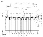
図1及び図3に示されるように、本実施の形態の半導体装置1の製造方法は、ウエハ2の第1主面2aの第2領域4にダイシング溝12を形成することを備える。複数の第1領域3に複数の半導体装置1をそれぞれ形成することの前または後に、ダイシング溝12が第2領域4に形成されてもよいし、複数の第1領域3に複数の半導体装置1をそれぞれ形成しながら、ダイシング溝12が第2領域4に形成されてもよい。ダイシング溝12は第2の方向(y方向)に沿って延在しており、かつ、複数の溝12a,12b,12c,12dを含む。   As shown in FIGS. 1 and 3, the manufacturing method of the semiconductor device 1 of the present embodiment includes forming a dicing groove 12 in the second region 4 of the first main surface 2 a of the wafer 2. Before or after forming the plurality of semiconductor devices 1 in the plurality of first regions 3, the dicing grooves 12 may be formed in the second region 4, or the plurality of semiconductor devices 1 may be formed in the plurality of first regions 3. The dicing groove 12 may be formed in the second region 4 while forming the respective layers. Dicing groove 12 extends in the second direction (y direction) and includes a plurality of grooves 12a, 12b, 12c, and 12d.

複数の溝12a,12b,12c,12dは、第1の方向(x方向)に沿って配列されており、かつ、第2の方向(y方向)に沿って延在している。一対の溝12a,12aは、第1の方向(x方向)における第2領域4の中心4cの最も近くに配置されている。溝12bは、溝12aに隣り合っており、かつ、溝12aに対して第2の領域の中心4cとは反対側にある。溝12cは、溝12bに隣り合っており、かつ、溝12bに対して第2の領域の中心4cとは反対側にある。溝12dは、溝12cに隣り合っており、かつ、溝12cに対して第2の領域の中心4cとは反対側にある。   The plurality of grooves 12a, 12b, 12c, 12d are arranged along a first direction (x direction) and extend along a second direction (y direction). The pair of grooves 12a is arranged closest to the center 4c of the second region 4 in the first direction (x direction). The groove 12b is adjacent to the groove 12a, and is on the opposite side of the groove 12a from the center 4c of the second region. The groove 12c is adjacent to the groove 12b, and is on the opposite side of the groove 12b from the center 4c of the second region. The groove 12d is adjacent to the groove 12c, and is on the opposite side of the groove 12c from the center 4c of the second region.

複数の溝12a,12b,12c,12dは、第1の方向(x方向)における第2領域4の両端4a,4bから、第1の方向(x方向)における第2領域4の中心4cに向かうにつれて、互いに隣り合う溝12a,12b,12c,12dの間の間隔D1,D2,D3,D4が減少するように形成されている。具体的には、溝12dと溝12cとの間の間隔D4は、溝12cと溝12bとの間の間隔D3よりも小さい。溝12cと溝12bとの間の間隔D3は、溝12bと溝12aとの間の間隔D2よりも小さい。溝12bと溝12aとの間の間隔D2は、第2領域4の中心4cに最も近い一対の溝12a,12aの間の間隔D1よりも小さい。 The plurality of grooves 12a, 12b, 12c, 12d extend from both ends 4a, 4b of the second region 4 in the first direction (x direction) to the center 4c of the second region 4 in the first direction (x direction). Accordingly, the distances D 1 , D 2 , D 3 , D 4 between the grooves 12a, 12b, 12c, 12d adjacent to each other are formed to decrease. Specifically, the distance D 4 between the groove 12d and the groove 12c is smaller than the distance D 3 between the grooves 12c and the groove 12b. Distance D between the grooves 12c and the groove 12b 3 is smaller than the distance D 2 between the groove 12b and the groove 12a. Interval D 2 between the groove 12b and the groove 12a is closest pair of grooves 12a in the center 4c of the second region 4 is smaller than the distance D 1 of the between 12a.

本実施の形態の半導体装置1の製造方法では、複数の溝12a,12b,12c,12dの幅T1,T2,T3,T4は、中心4cから両端4a,4bに向かうにつれて大きくなっている。具体的には、溝12bの幅T2は、第2領域4の中心4cに最も近い溝12aの幅T1よりも大きい。溝12cの幅T3は、溝12bの幅T2よりも大きい。溝12dの幅T4は、溝12cの幅T3よりも大きい。複数の溝12a,12b,12c,12dのうち第1の方向(x方向)における両端溝(溝12d)の各々の幅T4は、10μm以上である。複数の溝12a,12b,12c,12dは、例えば、第2領域4の中心4cに関して対称に形成されている。ダイシング溝12は、偶数個の溝12a,12b,12c,12dから構成されている。 In the method of manufacturing semiconductor device 1 of the present embodiment, widths T 1 , T 2 , T 3 , and T 4 of grooves 12a, 12b, 12c, and 12d increase from center 4c toward both ends 4a and 4b. ing. Specifically, the width T 2 of the grooves 12b is greater than the width T 1 of the nearest groove 12a in the center 4c of the second region 4. Width T 3 of the groove 12c is larger than the width T 2 of the grooves 12b. Width T 4 of the groove 12d is greater than the width T 3 of the groove 12c. A plurality of grooves 12a, 12b, 12c, each width T 4 of both ends grooves (grooves 12d) in a first direction of 12d (x direction) is 10μm or more. The plurality of grooves 12a, 12b, 12c, 12d are formed symmetrically with respect to the center 4c of the second region 4, for example. The dicing groove 12 includes an even number of grooves 12a, 12b, 12c, and 12d.

ダイシング溝12(複数の溝12a,12b,12c,12d)は、例えば、ウエハ2をエッチングすることによって形成される。ダイシング溝12(複数の溝12a,12b,12c,12d)は、複数の第1領域3に複数の半導体装置1をそれぞれ形成する際に複数の第1領域3に形成されるトレンチ34と一括して形成されてもよい。そのため、より少ない工程数で半導体装置1が製造され得る。   The dicing grooves 12 (the plurality of grooves 12a, 12b, 12c, 12d) are formed, for example, by etching the wafer 2. The dicing grooves 12 (the plurality of grooves 12a, 12b, 12c, and 12d) are collectively formed with the trenches 34 formed in the plurality of first regions 3 when the plurality of semiconductor devices 1 are formed in the plurality of first regions 3 respectively. May be formed. Therefore, the semiconductor device 1 can be manufactured with a smaller number of steps.

本実施の形態の半導体装置1の製造方法は、複数の溝12a,12b,12c,12dの表面に第1絶縁膜13を形成することを備える。第1絶縁膜13は、例えば、SiO2膜である。第1絶縁膜13は、例えば、複数の溝12a,12b,12c,12dの表面を熱酸化することによって形成される。第1絶縁膜13は、複数の第1領域3に複数の半導体装置1をそれぞれ形成する際に複数の第1領域3に形成される絶縁膜(例えば、ゲート絶縁膜35)と一括して形成されてもよい。そのため、より少ない工程数で半導体装置1が製造され得る。 The method for manufacturing the semiconductor device 1 according to the present embodiment includes forming the first insulating film 13 on the surfaces of the plurality of grooves 12a, 12b, 12c, and 12d. The first insulating film 13 is, for example, a SiO 2 film. The first insulating film 13 is formed, for example, by thermally oxidizing the surfaces of the plurality of grooves 12a, 12b, 12c, 12d. The first insulating film 13 is formed collectively with an insulating film (eg, a gate insulating film 35) formed in the plurality of first regions 3 when the plurality of semiconductor devices 1 are formed in the plurality of first regions 3 respectively. May be done. Therefore, the semiconductor device 1 can be manufactured with a smaller number of steps.

本実施の形態の半導体装置1の製造方法は、複数の溝12a,12b,12c,12d内に第1多結晶膜14を形成することを備える。第1多結晶膜14は、例えば、ポリシリコン膜である。第1多結晶膜14は、ウエハ2よりも機械的に脆弱である。第1多結晶膜14は、例えば、化学的気相成長法(CVD)または蒸着法を用いて形成される。第1多結晶膜14は、複数の第1領域3に複数の半導体装置1をそれぞれ形成する際に複数の第1領域3に形成される第2多結晶膜(例えば、ゲート電極36)と一括して形成されてもよい。そのため、より少ない工程数で半導体装置1が製造され得る。   The method for manufacturing the semiconductor device 1 of the present embodiment includes forming the first polycrystalline film 14 in the plurality of grooves 12a, 12b, 12c, 12d. The first polycrystalline film 14 is, for example, a polysilicon film. First polycrystalline film 14 is mechanically more fragile than wafer 2. The first polycrystalline film 14 is formed using, for example, a chemical vapor deposition (CVD) method or a vapor deposition method. The first polycrystalline film 14 is formed together with second polycrystalline films (eg, gate electrodes 36) formed in the plurality of first regions 3 when the plurality of semiconductor devices 1 are formed in the plurality of first regions 3 respectively. It may be formed as follows. Therefore, the semiconductor device 1 can be manufactured with a smaller number of steps.

本実施の形態の半導体装置1の製造方法は、ウエハ2の第1主面2aの第2領域4上に第2絶縁膜16を形成することを備える。第2絶縁膜16は、例えば、BPTEOS(Boro Phospho Tetra Ethyl Ortho Silicate glass)膜である。第2絶縁膜16は、例えば、化学的気相成長法(CVD)または蒸着法を用いて、第1主面2a上に形成される。第2絶縁膜16は、複数の第1領域3に複数の半導体装置1をそれぞれ形成する際に複数の第1領域3に形成される絶縁膜(例えば、層間絶縁膜37)と一括して形成されてもよい。そのため、より少ない工程数で半導体装置1が製造され得る。   The method for manufacturing semiconductor device 1 of the present embodiment includes forming second insulating film 16 on second region 4 of first main surface 2a of wafer 2. The second insulating film 16 is, for example, a BPTEOS (Boro Phospho Tetra Ethyl Ortho Silicate glass) film. The second insulating film 16 is formed on the first main surface 2a by using, for example, a chemical vapor deposition method (CVD) or a vapor deposition method. The second insulating film 16 is formed collectively with an insulating film (for example, an interlayer insulating film 37) formed in the plurality of first regions 3 when the plurality of semiconductor devices 1 are formed in the plurality of first regions 3 respectively. May be done. Therefore, the semiconductor device 1 can be manufactured with a smaller number of steps.

本実施の形態の半導体装置1の製造方法は、複数の第1領域3の各々の周縁部上に第1非晶質絶縁膜17を形成することを備える。複数の第1領域3の各々の周縁部は第2領域4(端4a,4b)に接している。第1非晶質絶縁膜17は、例えば、非晶質窒化シリコン膜または非晶質二酸化シリコン膜である。第1非晶質絶縁膜17は、例えば、化学的気相成長法(CVD)または蒸着法を用いて形成される。第1非晶質絶縁膜17は、複数の第1領域3に複数の半導体装置1をそれぞれ形成する際に複数の第1領域3に形成される非晶質絶縁膜(図示せず)と一括して形成されてもよい。   The method for manufacturing the semiconductor device 1 of the present embodiment includes forming the first amorphous insulating film 17 on each peripheral portion of the plurality of first regions 3. The periphery of each of the plurality of first regions 3 is in contact with the second region 4 (ends 4a and 4b). The first amorphous insulating film 17 is, for example, an amorphous silicon nitride film or an amorphous silicon dioxide film. The first amorphous insulating film 17 is formed by using, for example, a chemical vapor deposition (CVD) method or a vapor deposition method. The first amorphous insulating film 17 is formed together with an amorphous insulating film (not shown) formed in the plurality of first regions 3 when the plurality of semiconductor devices 1 are formed in the plurality of first regions 3. It may be formed as follows.

図3及び図4に示されるように、本実施の形態の半導体装置1の製造方法は、第2領域4にブレード20を押し当てながら、ダイシング溝12に沿ってブレード20をウエハ2に対して相対的に移動させることにより、ウエハ2を分割することを備える。ウエハ2の第1主面2aの平面視において、ブレード20の両側面20sは、複数の溝12a,12b,12c,12dのうち第1の方向(x方向)における両端溝(溝12d)にそれぞれ重なっている。第1の方向(x方向)におけるブレード20の中心20cは、第2領域4の中心4cに一致している。こうして、半導体装置1が得られる。   As shown in FIGS. 3 and 4, in the method of manufacturing the semiconductor device 1 of the present embodiment, the blade 20 is pressed against the wafer 2 along the dicing groove 12 while pressing the blade 20 against the second region 4. The method includes dividing the wafer 2 by relatively moving the wafer 2. In a plan view of the first main surface 2a of the wafer 2, both side surfaces 20s of the blade 20 are respectively positioned at both end grooves (grooves 12d) in the first direction (x direction) among the plurality of grooves 12a, 12b, 12c, and 12d. overlapping. The center 20c of the blade 20 in the first direction (x direction) coincides with the center 4c of the second region 4. Thus, the semiconductor device 1 is obtained.

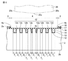
図5に示されるように、本実施の形態の第1変形例の半導体装置1の製造方法では、ダイシング溝12は、奇数個の溝12a,12b,12c,12dから構成されている。第1の方向(x方向)における溝12aの中心が第2領域4の中心4cに一致するように、溝12aが形成されている。   As shown in FIG. 5, in the method of manufacturing the semiconductor device 1 according to the first modification of the present embodiment, the dicing groove 12 includes an odd number of grooves 12a, 12b, 12c, and 12d. The groove 12a is formed such that the center of the groove 12a in the first direction (x direction) matches the center 4c of the second region 4.

図6に示されるように、本実施の形態の第2変形例の半導体装置1の製造方法は、ブレード20を用いてウエハ2を分割する前に、第1非晶質絶縁膜17上に第2非晶質絶縁膜18を形成することをさらに備える。第2非晶質絶縁膜18は、例えば、非晶質窒化シリコン膜または非晶質二酸化シリコン膜である。第2非晶質絶縁膜18は、第1非晶質絶縁膜17と同じ材料で構成されてもよいし、異なる材料で構成されてもよい。第2非晶質絶縁膜18は、例えば、化学的気相成長法(CVD)または蒸着法を用いて形成される。第2非晶質絶縁膜18は、複数の第1領域3に複数の半導体装置1をそれぞれ形成する際に複数の第1領域3に形成される非晶質絶縁膜(図示せず)と一括して形成されてもよい。   As shown in FIG. 6, in the method of manufacturing the semiconductor device 1 according to the second modification of the present embodiment, before the wafer 2 is divided using the blade 20, the first The method further includes forming the two amorphous insulating films 18. The second amorphous insulating film 18 is, for example, an amorphous silicon nitride film or an amorphous silicon dioxide film. The second amorphous insulating film 18 may be made of the same material as the first amorphous insulating film 17 or may be made of a different material. The second amorphous insulating film 18 is formed by using, for example, a chemical vapor deposition (CVD) method or an evaporation method. The second amorphous insulating film 18 is formed together with an amorphous insulating film (not shown) formed in the plurality of first regions 3 when the plurality of semiconductor devices 1 are formed in the plurality of first regions 3. It may be formed as follows.

本実施の形態の第3変形例の半導体装置1の製造方法は、ウエハ2の第1主面2aの第3領域5に第2ダイシング溝(図示せず)を形成することをさらに備える。第2ダイシング溝は第1の方向(x方向)に沿って延在しており、かつ、複数の第2溝(図示せず)を含む。複数の第2溝は、第2の方向(y方向)に沿って配列されており、かつ、第1の方向(x方向)に沿って延在している。第2ダイシング溝(複数の第2溝)は、ダイシング溝12(複数の溝12a,12b,12c,12d)と同じ構成を有している。   The method of manufacturing the semiconductor device 1 according to the third modification of the present embodiment further includes forming a second dicing groove (not shown) in the third region 5 of the first main surface 2a of the wafer 2. The second dicing groove extends along the first direction (x direction) and includes a plurality of second grooves (not shown). The plurality of second grooves are arranged along the second direction (y-direction) and extend along the first direction (x-direction). The second dicing groove (the plurality of second grooves) has the same configuration as the dicing groove 12 (the plurality of grooves 12a, 12b, 12c, 12d).

本実施の形態の半導体装置1の製造方法の効果を説明する。
本実施の形態の半導体装置1の製造方法は、ウエハ2の第1主面2aの複数の第1領域3に複数の半導体装置1をそれぞれ形成することを備える。複数の第1領域3は、第1の方向(x方向)と第1の方向(x方向)に交差する第2の方向(y方向)とに沿って配列されている。本実施の形態の半導体装置1の製造方法は、ウエハ2の第1主面2aの第2領域4にダイシング溝12を形成することをさらに備える。第2領域4は複数の第1領域3の間にあり、かつ、第2の方向(y方向)に沿って延在している。本実施の形態の半導体装置1の製造方法は、第2領域4にブレード20を押し当てながら、ダイシング溝12に沿ってブレード20をウエハ2に対して相対的に移動させることにより、ウエハ2を分割することを備える。ダイシング溝12は第2の方向(y方向)に沿って延在しており、かつ、複数の溝12a,12b,12c,12dを含む。複数の溝12a,12b,12c,12dは、第1の方向(x方向)に沿って配列されており、かつ、第2の方向(y方向)に沿って延在している。複数の溝12a,12b,12c,12dは、第1の方向(x方向)における第2領域4の両端4a,4bから、第1の方向(x方向)における第2領域4の中心4cに向かうにつれて、互いに隣り合う溝12a,12b,12c,12dの間の間隔D1,D2,D3,D4が減少するように形成されている。
The effect of the method for manufacturing the semiconductor device 1 of the present embodiment will be described.
The method for manufacturing the semiconductor device 1 according to the present embodiment includes forming the plurality of semiconductor devices 1 in the plurality of first regions 3 of the first main surface 2a of the wafer 2 respectively. The plurality of first regions 3 are arranged along a first direction (x direction) and a second direction (y direction) intersecting with the first direction (x direction). The method for manufacturing semiconductor device 1 of the present embodiment further includes forming dicing groove 12 in second region 4 of first main surface 2a of wafer 2. The second region 4 is between the plurality of first regions 3 and extends along the second direction (y direction). In the method of manufacturing the semiconductor device 1 according to the present embodiment, the wafer 2 is moved relative to the wafer 2 along the dicing groove 12 while pressing the blade 20 against the second region 4. Comprising splitting. Dicing groove 12 extends in the second direction (y direction) and includes a plurality of grooves 12a, 12b, 12c, and 12d. The plurality of grooves 12a, 12b, 12c, 12d are arranged along a first direction (x direction) and extend along a second direction (y direction). The plurality of grooves 12a, 12b, 12c, 12d extend from both ends 4a, 4b of the second region 4 in the first direction (x direction) to the center 4c of the second region 4 in the first direction (x direction). Accordingly, the gaps D 1 , D 2 , D 3 , D 4 between the adjacent grooves 12a, 12b, 12c, 12d are formed to decrease.

ウエハ2を分割する際、ブレード20はウエハ2に衝撃(機械的エネルギー)を加える。この衝撃は、ブレード20の中心20cに対応するウエハ2の第2領域4の中心4cにおいて最も大きい。複数の溝12a,12b,12c,12dは、第1の方向(x方向)における第2領域4の両端4a,4bから、第1の方向(x方向)における第2領域4の中心4cに向かうにつれて、互いに隣り合う溝12a,12b,12c,12dの間の間隔D1,D2,D3,D4が減少するように形成されている。ウエハ2の第2領域4は、第2領域4の中心4cにおいて最も脆い。ブレード20がウエハ2に加える衝撃が緩和されて、ウエハ2におけるチッピングの発生が減少され得る。さらに、複数の溝12a,12b,12c,12dは、各々、第1領域3に向けたチッピングの進行を阻止する、または、チッピングの進行方向を第1主面2aに向けて曲げる。こうして、半導体装置1が形成されているウエハ2の第1領域3にチッピングが到達することが抑制される。本実施の形態の半導体装置1の製造方法は、半導体装置1の収率を向上させることができる。 When dividing the wafer 2, the blade 20 applies an impact (mechanical energy) to the wafer 2. This impact is greatest at the center 4c of the second region 4 of the wafer 2 corresponding to the center 20c of the blade 20. The plurality of grooves 12a, 12b, 12c, 12d extend from both ends 4a, 4b of the second region 4 in the first direction (x direction) to the center 4c of the second region 4 in the first direction (x direction). Accordingly, the distances D 1 , D 2 , D 3 , D 4 between the grooves 12a, 12b, 12c, 12d adjacent to each other are formed to decrease. The second region 4 of the wafer 2 is the most fragile at the center 4c of the second region 4. The impact of the blade 20 on the wafer 2 is reduced, and the occurrence of chipping in the wafer 2 can be reduced. Further, each of the plurality of grooves 12a, 12b, 12c, and 12d prevents the progress of chipping toward the first region 3, or bends the direction of chipping toward the first main surface 2a. Thus, chipping is prevented from reaching the first region 3 of the wafer 2 on which the semiconductor device 1 is formed. The method for manufacturing the semiconductor device 1 according to the present embodiment can improve the yield of the semiconductor device 1.

また、複数の溝12a,12b,12c,12dは、ウエハ2の第1領域3にチッピングが到達することを抑制するため、第1の方向(x方向)における第2領域4の幅が減少され得る。1枚のウエハ2に、より多くの半導体装置1が形成され得る。1枚のウエハ2から得られる半導体装置1の収率は増加し、半導体装置1の製造コストは減少する。   In addition, the plurality of grooves 12a, 12b, 12c, and 12d reduce the width of the second region 4 in the first direction (x direction) in order to suppress chipping from reaching the first region 3 of the wafer 2. obtain. More semiconductor devices 1 can be formed on one wafer 2. The yield of the semiconductor device 1 obtained from one wafer 2 increases, and the manufacturing cost of the semiconductor device 1 decreases.

本実施の形態の半導体装置1の製造方法では、複数の溝12a,12b,12c,12dの幅T1,T2,T3,T4は、第2領域4の中心4cから両端4a,4bに向かうにつれて大きくなっている。第1の方向(x方向)における両端溝(溝12d)は、複数の溝12a,12b,12c,12dの中で最も大きい幅を有しており、第1領域3に向けたチッピングの進行を最も確実に阻止することができる。半導体装置1が形成されているウエハ2の第1領域3にチッピングが到達することが抑制される。本実施の形態の半導体装置1の製造方法は、半導体装置1の収率を向上させることができる。 In the method of manufacturing the semiconductor device 1 according to the present embodiment, the widths T 1 , T 2 , T 3 , and T 4 of the plurality of grooves 12 a, 12 b, 12 c, and 12 d are both ends 4 a and 4 b from the center 4 c of the second region 4. It is getting bigger toward. Both end grooves (grooves 12 d) in the first direction (x direction) have the largest width among the plurality of grooves 12 a, 12 b, 12 c, and 12 d, so that the chipping toward the first region 3 proceeds. It can be prevented most reliably. Chipping is prevented from reaching the first region 3 of the wafer 2 on which the semiconductor device 1 is formed. The method for manufacturing the semiconductor device 1 according to the present embodiment can improve the yield of the semiconductor device 1.

さらに、第1の方向(x方向)における両端溝(溝12d)は、複数の溝12a,12b,12c,12dの中で、最も大きい幅を有しているため、ブレード20の両側面20sと両端溝(溝12d)との間の位置合わせが容易になる。ブレード20を用いてウエハ2を分割する際に第1主面2aにバリが発生することが抑制され、かつ、半導体装置1がより短時間で製造され得る。   Further, since both end grooves (grooves 12d) in the first direction (x direction) have the largest width among the plurality of grooves 12a, 12b, 12c, and 12d, the both side surfaces 20s of the blade 20 are in contact with each other. Positioning between the grooves at both ends (grooves 12d) is facilitated. When dividing the wafer 2 using the blade 20, the generation of burrs on the first main surface 2a is suppressed, and the semiconductor device 1 can be manufactured in a shorter time.

本実施の形態の半導体装置1の製造方法は、ウエハ2の第1主面2aの複数の第1領域3に複数の半導体装置1をそれぞれ形成することを備える。複数の第1領域3は、第1の方向(x方向)と第1の方向(x方向)に交差する第2の方向(y方向)とに沿って配列されている。本実施の形態の半導体装置1の製造方法は、ウエハ2の第1主面2aの第2領域4にダイシング溝12を形成することをさらに備える。第2領域4は複数の第1領域3の間にあり、かつ、第2の方向(y方向)に沿って延在している。本実施の形態の半導体装置1の製造方法は、第2領域4にブレード20を押し当てながら、ダイシング溝12に沿ってブレード20をウエハ2に対して相対的に移動させることにより、ウエハ2を分割することを備える。ダイシング溝12は第2の方向(y方向)に沿って延在しており、かつ、複数の溝12a,12b,12c,12dを含む。複数の溝12a,12b,12c,12dは、第1の方向(x方向)に沿って配列されており、かつ、第2の方向(y方向)に沿って延在している。第1の方向(x方向)における複数の溝12a,12b,12c,12dの幅T1,T2,T3,T4は、第1の方向(x方向)における第2領域4の中心4cから、第1の方向(x方向)における第2領域4の両端4a,4bに向かうにつれて大きくなっている。 The method for manufacturing the semiconductor device 1 according to the present embodiment includes forming the plurality of semiconductor devices 1 in the plurality of first regions 3 of the first main surface 2a of the wafer 2 respectively. The plurality of first regions 3 are arranged along a first direction (x direction) and a second direction (y direction) intersecting with the first direction (x direction). The method for manufacturing semiconductor device 1 of the present embodiment further includes forming dicing groove 12 in second region 4 of first main surface 2a of wafer 2. The second region 4 is between the plurality of first regions 3 and extends along the second direction (y direction). In the method of manufacturing the semiconductor device 1 according to the present embodiment, the wafer 2 is moved relative to the wafer 2 along the dicing groove 12 while pressing the blade 20 against the second region 4. Comprising splitting. Dicing groove 12 extends in the second direction (y direction) and includes a plurality of grooves 12a, 12b, 12c, and 12d. The plurality of grooves 12a, 12b, 12c, 12d are arranged along a first direction (x direction) and extend along a second direction (y direction). A plurality of grooves 12a in the first direction (x-direction), 12b, 12c, the width T 1 of the 12d, T 2, T 3, T 4, the first direction center 4c of the second region 4 in the (x-direction) And becomes larger toward both ends 4a and 4b of the second region 4 in the first direction (x direction).

第1の方向(x方向)における両端溝(溝12d)は、複数の溝12a,12b,12c,12dの中で最も大きい幅を有しており、第1領域3に向けたチッピングの進行を最も確実に阻止することができる。さらに、複数の溝12a,12b,12c,12dのうち両端溝(溝12d)以外の溝12a,12b,12cは、ブレード20がウエハ2に加える衝撃を緩和し、ウエハ2におけるチッピングの発生を減少させる。半導体装置1が形成されているウエハ2の第1領域3にチッピングが到達することが抑制される。本実施の形態の半導体装置1の製造方法は、半導体装置1の収率を向上させることができる。   Both end grooves (grooves 12 d) in the first direction (x direction) have the largest width among the plurality of grooves 12 a, 12 b, 12 c, and 12 d, so that the chipping toward the first region 3 proceeds. It can be prevented most reliably. Further, the grooves 12a, 12b, 12c other than the two-end grooves (grooves 12d) out of the plurality of grooves 12a, 12b, 12c, 12d reduce the impact of the blade 20 on the wafer 2 and reduce the occurrence of chipping in the wafer 2. Let it. Chipping is prevented from reaching the first region 3 of the wafer 2 on which the semiconductor device 1 is formed. The method for manufacturing the semiconductor device 1 according to the present embodiment can improve the yield of the semiconductor device 1.

さらに、第1の方向(x方向)における両端溝(溝12d)は、複数の溝12a,12b,12c,12dの中で、最も大きい幅を有しているため、ブレード20の両側面20sと両端溝(溝12d)との間の位置合わせが容易になる。ブレード20を用いてウエハ2を分割する際に第1主面2aにバリが発生することが抑制され、かつ、半導体装置1がより短時間で製造され得る。   Further, since both end grooves (grooves 12d) in the first direction (x direction) have the largest width among the plurality of grooves 12a, 12b, 12c, and 12d, the both side surfaces 20s of the blade 20 are in contact with each other. Positioning between the grooves at both ends (grooves 12d) is facilitated. When dividing the wafer 2 using the blade 20, the generation of burrs on the first main surface 2a is suppressed, and the semiconductor device 1 can be manufactured in a shorter time.

本実施の形態の半導体装置1の製造方法では、ウエハ2の第1主面2aの平面視において、ブレード20の両側面20sは、複数の溝12a,12b,12c,12dのうち第1の方向(x方向)における両端溝(溝12d)にそれぞれ重なっている。そのため、ブレード20を用いてウエハ2を分割する際に第1主面2aにバリが発生することが抑制される。   In the method for manufacturing semiconductor device 1 of the present embodiment, both sides 20s of blade 20 are in the first direction among grooves 12a, 12b, 12c, and 12d in plan view of first main surface 2a of wafer 2. Each groove overlaps with both end grooves (groove 12d) in the (x direction). Therefore, when the wafer 2 is divided using the blade 20, generation of burrs on the first main surface 2 a is suppressed.

本実施の形態の半導体装置1の製造方法では、複数の溝12a,12b,12c,12dのうち第1の方向(x方向)における両端溝(溝12d)は、各々、10μm以上の幅T4を有している。そのため、ブレード20の両側面20sと両端溝(溝12d)との間の位置合わせが容易になる。ブレード20を用いてウエハ2を分割する際に第1主面2aにバリが発生することが抑制され、かつ、半導体装置1がより短時間で製造され得る。 In the manufacturing method of the semiconductor device 1 of this embodiment, a plurality of grooves 12a, 12b, 12c, both end grooves (grooves 12d) in a first direction (x-direction) of the 12d, respectively, the width T 4 10 [mu] m or more have. Therefore, alignment between the both side surfaces 20s of the blade 20 and both end grooves (grooves 12d) becomes easy. When dividing the wafer 2 using the blade 20, the generation of burrs on the first main surface 2a is suppressed, and the semiconductor device 1 can be manufactured in a shorter time.

本実施の形態の半導体装置1の製造方法では、複数の溝12a,12b,12c,12dは、複数の第1領域3に複数の半導体装置1をそれぞれ形成する際に複数の第1領域3に形成されるトレンチ(例えば、トレンチゲート構造を有するIGBTに形成されるトレンチ34)と一括して形成されてもよい。本実施の形態の半導体装置1の製造方法によれば、より少ない工程数で半導体装置1が製造され得る。   In the method of manufacturing the semiconductor device 1 according to the present embodiment, the plurality of grooves 12a, 12b, 12c, and 12d are formed in the plurality of first regions 3 when the plurality of semiconductor devices 1 are formed in the plurality of first regions 3, respectively. It may be formed together with the formed trench (for example, the trench 34 formed in the IGBT having the trench gate structure). According to the method of manufacturing semiconductor device 1 of the present embodiment, semiconductor device 1 can be manufactured with a smaller number of steps.

本実施の形態の半導体装置1の製造方法は、複数の第1領域3の各々の周縁部上に第1非晶質絶縁膜17を形成することをさらに備える。周縁部は第2領域4に接している。複数の第1領域3の各々の周縁部の厚さが増加し、複数の第1領域3の各々の周縁部の機械的強度が増加する。半導体装置1が形成されているウエハ2の第1領域3にチッピングが到達することがさらに抑制される。本実施の形態の半導体装置1の製造方法は、半導体装置1の収率を向上させることができる。   The method for manufacturing the semiconductor device 1 according to the present embodiment further includes forming the first amorphous insulating film 17 on the peripheral portion of each of the plurality of first regions 3. The peripheral portion is in contact with the second region 4. The thickness of each peripheral edge of the plurality of first regions 3 increases, and the mechanical strength of each peripheral edge of each of the plurality of first regions 3 increases. Chipping is further suppressed from reaching the first region 3 of the wafer 2 on which the semiconductor device 1 is formed. The method for manufacturing the semiconductor device 1 according to the present embodiment can improve the yield of the semiconductor device 1.

また、第1非晶質絶縁膜17は、複数の溝12a,12b,12c,12dとともに、ウエハ2の第1領域3にチッピングが到達することを抑制するため、第1の方向(x方向)におけるウエハ2の第2領域4の幅がさらに減少され得る。1枚のウエハ2に、より多くの半導体装置1が形成され得る。1枚のウエハ2から得られる半導体装置1の収率は増加し、半導体装置1の製造コストは減少する。   The first amorphous insulating film 17 is formed in the first direction (x direction) in order to prevent chipping from reaching the first region 3 of the wafer 2 together with the plurality of grooves 12a, 12b, 12c, and 12d. Can be further reduced. More semiconductor devices 1 can be formed on one wafer 2. The yield of the semiconductor device 1 obtained from one wafer 2 increases, and the manufacturing cost of the semiconductor device 1 decreases.

本実施の形態の半導体装置1の製造方法は、第1非晶質絶縁膜17上に第2非晶質絶縁膜18を形成することをさらに備える。複数の第1領域3の各々の周縁部の厚さが増加し、複数の第1領域3の各々の周縁部の機械的強度が増加する。半導体装置1が形成されているウエハ2の第1領域3にチッピングが到達することがさらに抑制される。本実施の形態の半導体装置1の製造方法は、半導体装置1の収率を向上させることができる。   The method for manufacturing the semiconductor device 1 of the present embodiment further includes forming a second amorphous insulating film 18 on the first amorphous insulating film 17. The thickness of each peripheral edge of the plurality of first regions 3 increases, and the mechanical strength of each peripheral edge of each of the plurality of first regions 3 increases. Chipping is further suppressed from reaching the first region 3 of the wafer 2 on which the semiconductor device 1 is formed. The method for manufacturing the semiconductor device 1 according to the present embodiment can improve the yield of the semiconductor device 1.

また、第2非晶質絶縁膜18は、複数の溝12a,12b,12c,12d及び第1非晶質絶縁膜17とともに、ウエハ2の第1領域3にチッピングが到達することを抑制するため、第1の方向(x方向)におけるウエハ2の第2領域4の幅がさらに減少され得る。1枚のウエハ2に、より多くの半導体装置1が形成され得る。1枚のウエハ2から得られる半導体装置1の収率は増加し、半導体装置1の製造コストは減少する。   Further, the second amorphous insulating film 18, together with the plurality of grooves 12 a, 12 b, 12 c, 12 d and the first amorphous insulating film 17, is for suppressing chipping from reaching the first region 3 of the wafer 2. The width of the second region 4 of the wafer 2 in the first direction (x direction) can be further reduced. More semiconductor devices 1 can be formed on one wafer 2. The yield of the semiconductor device 1 obtained from one wafer 2 increases, and the manufacturing cost of the semiconductor device 1 decreases.

実施の形態2.
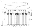
図1、図2及び図7から図9を参照して、実施の形態2の半導体装置1の製造方法を説明する。図7を参照して、本実施の形態の半導体装置1の製造方法は、実施の形態1の半導体装置1の製造方法と同様の工程を備え、同様の効果を奏するが、以下の点で主に異なる。本実施の形態の半導体装置1の製造方法では、複数の溝12a,12b,12c,12dは、互いに同じ幅T1,T2,T3,T4を有している。具体的には、溝12bの幅T2は、第2領域4の中心4cに最も近い溝12aの幅T1に等しい。溝12cの幅T3は、溝12bの幅T2に等しい。溝12dの幅T4は、溝12cの幅T3に等しい。
Embodiment 2 FIG.
The method of manufacturing the semiconductor device 1 according to the second embodiment will be described with reference to FIGS. Referring to FIG. 7, the method of manufacturing semiconductor device 1 of the present embodiment includes the same steps as the method of manufacturing semiconductor device 1 of the first embodiment, and achieves the same effects. Different. In the manufacturing method of the semiconductor device 1 of this embodiment, a plurality of grooves 12a, 12b, 12c, 12d have the same width T 1, T 2, T 3 , T 4 together. Specifically, the width T 2 of the grooves 12b is equal to the width T 1 of the nearest groove 12a in the center 4c of the second region 4. Width T 3 of the groove 12c is equal to the width T 2 of the grooves 12b. Width T 4 of the groove 12d is equal to the width T 3 of the groove 12c.

図8に示されるように、本実施の形態の第1変形例の半導体装置1の製造方法では、実施の形態1の第1変形例の半導体装置1の製造方法と同様に、ダイシング溝12は、奇数個の溝12a,12b,12c,12dから構成されている。第1の方向(x方向)における溝12aの中心が第2領域4の中心4cに一致するように、溝12aが形成されている。図9に示されるように、本実施の形態の第2変形例の半導体装置1の製造方法は、実施の形態1の第2変形例の半導体装置1の製造方法と同様に、ブレード20を用いてウエハ2を分割する前に、第1非晶質絶縁膜17上に第2非晶質絶縁膜18を形成することをさらに備える。   As shown in FIG. 8, in the method of manufacturing semiconductor device 1 of the first modification of the present embodiment, dicing groove 12 is formed similarly to the method of manufacturing semiconductor device 1 of the first modification of the first embodiment. , An odd number of grooves 12a, 12b, 12c, 12d. The groove 12a is formed such that the center of the groove 12a in the first direction (x direction) matches the center 4c of the second region 4. As shown in FIG. 9, the method of manufacturing the semiconductor device 1 of the second modification of the present embodiment uses the blade 20 similarly to the method of manufacturing the semiconductor device 1 of the second modification of the first embodiment. Forming a second amorphous insulating film on the first amorphous insulating film before the wafer is divided.

実施の形態3.
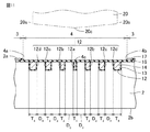
図1、図2及び図10から図12を参照して、実施の形態3の半導体装置1の製造方法を説明する。図10を参照して、本実施の形態の半導体装置1の製造方法は、実施の形態1の半導体装置1の製造方法と同様の工程を備え、同様の効果を奏するが、以下の点で主に異なる。本実施の形態の半導体装置1の製造方法では、互いに隣り合う溝12a,12b,12c,12dの間の間隔D1,D2,D3,D4が等しい。具体的には、溝12dと溝12cとの間の間隔D4は、溝12cと溝12bとの間の間隔D3に等しい。溝12cと溝12bとの間の間隔D3は、溝12bと溝12aとの間の間隔D2に等しい。溝12bと溝12aとの間の間隔D2は、第2領域4の中心4cに最も近い一対の溝12a,12aの間の間隔D1に等しい。
Embodiment 3 FIG.
A method of manufacturing the semiconductor device 1 according to the third embodiment will be described with reference to FIGS. 1, 2, and 10 to 12. Referring to FIG. 10, the method of manufacturing semiconductor device 1 of the present embodiment includes the same steps as the method of manufacturing semiconductor device 1 of the first embodiment, and achieves the same effects. Different. In the method for manufacturing the semiconductor device 1 of the present embodiment, the intervals D 1 , D 2 , D 3 , and D 4 between the grooves 12a, 12b, 12c, and 12d adjacent to each other are equal. Specifically, the distance D 4 between the groove 12d and the groove 12c is equal to the distance D 3 between the grooves 12c and the groove 12b. Distance D 3 between the grooves 12c and the groove 12b is equal to the distance D 2 between the groove 12b and the groove 12a. Interval D 2 between the groove 12b and the groove 12a is closest pair of grooves 12a in the center 4c of the second region 4, equal to the spacing D 1 of the between 12a.

図11に示されるように、本実施の形態の第1変形例の半導体装置1の製造方法では、実施の形態1の第1変形例の半導体装置1の製造方法と同様に、ダイシング溝12は、奇数個の溝12a,12b,12c,12dから構成されている。第1の方向(x方向)における溝12aの中心が第2領域4の中心4cに一致するように、溝12aが形成されている。図12に示されるように、本実施の形態の第2変形例の半導体装置1の製造方法は、実施の形態1の第2変形例の半導体装置1の製造方法と同様に、ブレード20を用いてウエハ2を分割する前に、第1非晶質絶縁膜17上に第2非晶質絶縁膜18を形成することをさらに備える。   As shown in FIG. 11, in the method of manufacturing semiconductor device 1 of the first modification of the present embodiment, dicing groove 12 is formed similarly to the method of manufacturing semiconductor device 1 of the first modification of the first embodiment. , An odd number of grooves 12a, 12b, 12c, 12d. The groove 12a is formed such that the center of the groove 12a in the first direction (x direction) matches the center 4c of the second region 4. As shown in FIG. 12, the method of manufacturing the semiconductor device 1 of the second modification of the present embodiment uses the blade 20 in the same manner as the method of manufacturing the semiconductor device 1 of the second modification of the first embodiment. Forming a second amorphous insulating film on the first amorphous insulating film before the wafer is divided.

今回開示された実施の形態1から実施の形態3はすべての点で例示であって制限的なものではないと考えられるべきである。本発明の範囲は、上記した説明ではなく特許請求の範囲によって示され、特許請求の範囲と均等の意味および範囲内でのすべての変更が含まれることを意図される。   The first to third embodiments disclosed this time are to be considered in all respects as illustrative and not restrictive. The scope of the present invention is defined by the terms of the claims, rather than the description above, and is intended to include any modifications within the scope and meaning equivalent to the terms of the claims.

1 半導体装置、2 ウエハ、2a 第1主面、2b 第2主面、3 第1領域、4 第2領域、4a,4b 端、4c 中心、5 第3領域、12 ダイシング溝、12a,12b,12c,12d 溝、13 第1絶縁膜、14 第1多結晶膜、16 第2絶縁膜、17 第1非晶質絶縁膜、18 第2非晶質絶縁膜、20 ブレード、20c 中心、20s 側面、30 n型ドリフト領域、31 p型ベース領域、31a 部分、32 n型エミッタ領域、33 p型コンタクト層、34 トレンチ、35 ゲート絶縁膜、36 ゲート電極、37 層間絶縁膜、38 エミッタ電極、39 コレクタ電極、40 n型バッファ領域、41 p型コレクタ層。   DESCRIPTION OF SYMBOLS 1 Semiconductor device, 2 wafer, 2a 1st main surface, 2b 2nd main surface, 3rd area, 4th area, 4a, 4b edge, 4c center, 5th area, 12 dicing groove, 12a, 12b, 12c, 12d groove, 13 first insulating film, 14 first polycrystalline film, 16 second insulating film, 17 first amorphous insulating film, 18 second amorphous insulating film, 20 blade, 20c center, 20s side surface , 30 n-type drift region, 31 p-type base region, 31 a portion, 32 n-type emitter region, 33 p-type contact layer, 34 trench, 35 gate insulating film, 36 gate electrode, 37 interlayer insulating film, 38 emitter electrode, 39 Collector electrode, 40 n-type buffer region, 41 p-type collector layer.

Claims (10)

ウエハの主面の複数の第1領域に複数の半導体装置をそれぞれ形成することを備え、前記複数の第1領域は、第1の方向と前記第1の方向に交差する第2の方向とに沿って配列されており、
前記ウエハの前記主面の第2領域にダイシング溝を形成することを備え、前記第2領域は前記複数の第1領域の間にあり、かつ、前記第2の方向に沿って延在しており、さらに、
前記第2領域にブレードを押し当てながら、前記ダイシング溝に沿って前記ブレードを前記ウエハに対して相対的に移動させることにより、前記ウエハを分割することを備え、
前記ダイシング溝は前記第2の方向に沿って延在しており、かつ、複数の溝を含み、
前記複数の溝は、前記第1の方向に沿って配列されており、かつ、前記第2の方向に沿って延在しており、
前記複数の溝は、前記第1の方向における前記第2領域の両端から前記第1の方向における前記第2領域の中心に向かうにつれて、互いに隣り合う前記溝の間の間隔が減少するように形成されている、半導体装置の製造方法。
Forming a plurality of semiconductor devices in a plurality of first regions on a main surface of the wafer, wherein the plurality of first regions are formed in a first direction and a second direction intersecting the first direction; Are arranged along
Forming a dicing groove in a second region of the main surface of the wafer, wherein the second region is between the plurality of first regions and extends along the second direction. And,
While pressing the blade against the second region, the wafer is divided along the dicing groove by moving the blade relative to the wafer,
The dicing groove extends along the second direction, and includes a plurality of grooves,
The plurality of grooves are arranged along the first direction, and extend along the second direction,
The plurality of grooves are formed such that an interval between the adjacent grooves decreases from both ends of the second region in the first direction toward a center of the second region in the first direction. Method for manufacturing a semiconductor device.
前記複数の溝の幅は、前記中心から前記両端に向かうにつれて大きくなっている、請求項1に記載の半導体装置の製造方法。   2. The method according to claim 1, wherein a width of the plurality of grooves increases from the center toward the ends. 3. ウエハの主面の複数の第1領域に複数の半導体装置をそれぞれ形成することを備え、前記複数の第1領域は、第1の方向と前記第1の方向に交差する第2の方向とに沿って配列されており、
前記ウエハの前記主面の第2領域にダイシング溝を形成することを備え、前記第2領域は前記複数の第1領域の間にあり、かつ、前記第2の方向に沿って延在しており、さらに、
前記第2領域にブレードを押し当てながら、前記ダイシング溝に沿って前記ブレードを前記ウエハに対して相対的に移動させることにより、前記ウエハを分割することを備え、
前記ダイシング溝は前記第2の方向に沿って延在しており、かつ、複数の溝を含み、
前記複数の溝は、前記第1の方向に沿って配列されており、かつ、前記第2の方向に沿って延在しており、
前記第1の方向における前記複数の溝の幅は、前記第1の方向における前記第2領域の中心から、前記第1の方向における前記第2領域の両端に向かうにつれて大きくなっている、半導体装置の製造方法。
Forming a plurality of semiconductor devices in a plurality of first regions on a main surface of the wafer, wherein the plurality of first regions are formed in a first direction and a second direction intersecting the first direction; Are arranged along
Forming a dicing groove in a second region of the main surface of the wafer, wherein the second region is between the plurality of first regions and extends along the second direction. And,
While pressing the blade against the second region, the wafer is divided along the dicing groove by moving the blade relative to the wafer,
The dicing groove extends along the second direction, and includes a plurality of grooves,
The plurality of grooves are arranged along the first direction, and extend along the second direction,
A width of the plurality of grooves in the first direction increases from a center of the second region in the first direction toward both ends of the second region in the first direction; Manufacturing method.
前記主面の平面視において、前記ブレードの両側面は、前記複数の溝のうち前記第1の方向における両端溝にそれぞれ重なっている、請求項1から請求項3のいずれか1項に記載の半導体装置の製造方法。   4. The device according to claim 1, wherein, in a plan view of the main surface, both side surfaces of the blade respectively overlap both end grooves in the first direction among the plurality of grooves. 5. A method for manufacturing a semiconductor device. 前記両端溝は、各々、10μm以上の幅を有している、請求項4に記載の半導体装置の製造方法。   The method for manufacturing a semiconductor device according to claim 4, wherein each of the two end grooves has a width of 10 μm or more. 前記複数の溝は、前記複数の第1領域に前記複数の半導体装置をそれぞれ形成する際に前記複数の第1領域に形成されるトレンチと一括して形成される、請求項1から請求項5のいずれか1項に記載の半導体装置の製造方法。   6. The plurality of trenches are formed together with trenches formed in the plurality of first regions when the plurality of semiconductor devices are formed in the plurality of first regions, respectively. 13. The method for manufacturing a semiconductor device according to claim 1. 前記複数の溝内に、第1多結晶膜を形成することをさらに備える、請求項1から請求項6のいずれか1項に記載の半導体装置の製造方法。   The method of manufacturing a semiconductor device according to claim 1, further comprising forming a first polycrystalline film in the plurality of grooves. 前記第1多結晶膜は、前記複数の第1領域に前記複数の半導体装置をそれぞれ形成する際に前記複数の第1領域に形成される第2多結晶膜と一括して形成される、請求項7に記載の半導体装置の製造方法。   The first polycrystalline film is formed together with a second polycrystalline film formed in the plurality of first regions when the plurality of semiconductor devices are formed in the plurality of first regions, respectively. Item 8. A method for manufacturing a semiconductor device according to item 7. 前記複数の第1領域の各々の周縁部上に第1非晶質絶縁膜を形成することをさらに備え、
前記周縁部は前記第2領域に接している、請求項1から請求項8のいずれか1項に記載の半導体装置の製造方法。
Further comprising forming a first amorphous insulating film on a peripheral portion of each of the plurality of first regions,
The method according to claim 1, wherein the peripheral portion is in contact with the second region.
前記第1非晶質絶縁膜上に第2非晶質絶縁膜を形成することをさらに備える、請求項9に記載の半導体装置の製造方法。
The method according to claim 9, further comprising forming a second amorphous insulating film on the first amorphous insulating film.
JP2018123889A 2018-06-29 2018-06-29 Manufacturing method of semiconductor devices Active JP6932109B2 (en)

Priority Applications (1)

Application Number Priority Date Filing Date Title
JP2018123889A JP6932109B2 (en) 2018-06-29 2018-06-29 Manufacturing method of semiconductor devices

Applications Claiming Priority (1)

Application Number Priority Date Filing Date Title
JP2018123889A JP6932109B2 (en) 2018-06-29 2018-06-29 Manufacturing method of semiconductor devices

Publications (2)

Publication Number Publication Date
JP2020004881A true JP2020004881A (en) 2020-01-09
JP6932109B2 JP6932109B2 (en) 2021-09-08

Family

ID=69100420

Family Applications (1)

Application Number Title Priority Date Filing Date
JP2018123889A Active JP6932109B2 (en) 2018-06-29 2018-06-29 Manufacturing method of semiconductor devices

Country Status (1)

Country Link
JP (1) JP6932109B2 (en)

Cited By (2)

* Cited by examiner, † Cited by third party
Publication number Priority date Publication date Assignee Title
JP2023109269A (en) * 2022-01-27 2023-08-08 三菱電機株式会社 SEMICONDUCTOR DEVICE, SEMICONDUCTOR DEVICE MANUFACTURING METHOD, AND POWER CONVERTER
JP2023147754A (en) * 2022-03-30 2023-10-13 株式会社豊田中央研究所 Semiconductor device manufacturing method and appearance inspection device for semiconductor devices

Citations (7)

* Cited by examiner, † Cited by third party
Publication number Priority date Publication date Assignee Title
JPH065701A (en) * 1992-06-23 1994-01-14 Fujitsu Ltd Manufacture of semiconductor device
JP2000252266A (en) * 1999-03-04 2000-09-14 Toshiba Corp Semiconductor device
JP2004055852A (en) * 2002-07-19 2004-02-19 Ricoh Co Ltd Semiconductor device and manufacturing method thereof
JP2005064231A (en) * 2003-08-12 2005-03-10 Disco Abrasive Syst Ltd How to divide a plate
JP2011119324A (en) * 2009-12-01 2011-06-16 Fujitsu Semiconductor Ltd Semiconductor device and method of manufacturing the same
JP2011192954A (en) * 2010-02-22 2011-09-29 Sanken Electric Co Ltd Semiconductor wafer and method of manufacturing semiconductor device
JP2016164942A (en) * 2015-03-06 2016-09-08 ラピスセミコンダクタ株式会社 Manufacturing method of semiconductor device and semiconductor laminate structure

Patent Citations (7)

* Cited by examiner, † Cited by third party
Publication number Priority date Publication date Assignee Title
JPH065701A (en) * 1992-06-23 1994-01-14 Fujitsu Ltd Manufacture of semiconductor device
JP2000252266A (en) * 1999-03-04 2000-09-14 Toshiba Corp Semiconductor device
JP2004055852A (en) * 2002-07-19 2004-02-19 Ricoh Co Ltd Semiconductor device and manufacturing method thereof
JP2005064231A (en) * 2003-08-12 2005-03-10 Disco Abrasive Syst Ltd How to divide a plate
JP2011119324A (en) * 2009-12-01 2011-06-16 Fujitsu Semiconductor Ltd Semiconductor device and method of manufacturing the same
JP2011192954A (en) * 2010-02-22 2011-09-29 Sanken Electric Co Ltd Semiconductor wafer and method of manufacturing semiconductor device
JP2016164942A (en) * 2015-03-06 2016-09-08 ラピスセミコンダクタ株式会社 Manufacturing method of semiconductor device and semiconductor laminate structure

Cited By (4)

* Cited by examiner, † Cited by third party
Publication number Priority date Publication date Assignee Title
JP2023109269A (en) * 2022-01-27 2023-08-08 三菱電機株式会社 SEMICONDUCTOR DEVICE, SEMICONDUCTOR DEVICE MANUFACTURING METHOD, AND POWER CONVERTER
JP7721220B2 (en) 2022-01-27 2025-08-12 三菱電機株式会社 Semiconductor device, semiconductor device manufacturing method, and power conversion device
JP2023147754A (en) * 2022-03-30 2023-10-13 株式会社豊田中央研究所 Semiconductor device manufacturing method and appearance inspection device for semiconductor devices
JP7796572B2 (en) 2022-03-30 2026-01-09 株式会社豊田中央研究所 Semiconductor device manufacturing method and visual inspection device for semiconductor device

Also Published As

Publication number Publication date
JP6932109B2 (en) 2021-09-08

Similar Documents

Publication Publication Date Title
JP5799046B2 (en) Semiconductor device
JP6284314B2 (en) Semiconductor device
JP6728953B2 (en) Semiconductor device and manufacturing method thereof
US11043582B2 (en) Semiconductor device
CN107180855B (en) Semiconductor device with a plurality of semiconductor chips
CN102254827B (en) Manufacture the method for super-junction semiconductor device
JP2023153392A (en) semiconductor equipment
JP5498107B2 (en) Semiconductor device and manufacturing method thereof
JP2012204529A (en) Semiconductor device and method of manufacturing the same
JP6616878B2 (en) Semiconductor device
WO2021210293A1 (en) Semiconductor device and method for manufacturing semiconductor device
JP7487756B2 (en) Semiconductor device and method for manufacturing the same
CN115376917A (en) Reverse blocking IGBT
JP2016039170A (en) Semiconductor device
US10236368B2 (en) Semiconductor device and method for manufacturing the same
JP6932109B2 (en) Manufacturing method of semiconductor devices
JP7319754B2 (en) semiconductor equipment
JP5446297B2 (en) Manufacturing method of semiconductor device
JP2016174027A (en) Semiconductor device
WO2021049351A1 (en) Semiconductor device
CN117855259A (en) Semiconductor device and method for manufacturing the same
JP7471250B2 (en) Semiconductor Device
JP2023056697A (en) Semiconductor device and its manufacturing method
JP7069646B2 (en) Semiconductor device
JP7763356B2 (en) METHOD FOR MANUFACTURING A SEMICONDUCTOR DEVICE AND SEMICONDUCTOR DEVICE - Patent application

Legal Events

Date Code Title Description
A621 Written request for application examination

Free format text: JAPANESE INTERMEDIATE CODE: A621

Effective date: 20200702

A977 Report on retrieval

Free format text: JAPANESE INTERMEDIATE CODE: A971007

Effective date: 20210707

TRDD Decision of grant or rejection written
A01 Written decision to grant a patent or to grant a registration (utility model)

Free format text: JAPANESE INTERMEDIATE CODE: A01

Effective date: 20210720

A61 First payment of annual fees (during grant procedure)

Free format text: JAPANESE INTERMEDIATE CODE: A61

Effective date: 20210817

R150 Certificate of patent or registration of utility model

Ref document number: 6932109

Country of ref document: JP

Free format text: JAPANESE INTERMEDIATE CODE: R150

R250 Receipt of annual fees

Free format text: JAPANESE INTERMEDIATE CODE: R250

R250 Receipt of annual fees

Free format text: JAPANESE INTERMEDIATE CODE: R250