JP2020004890A - Method and apparatus for cutting bonded substrates - Google Patents
Method and apparatus for cutting bonded substrates Download PDFInfo
- Publication number
- JP2020004890A JP2020004890A JP2018124059A JP2018124059A JP2020004890A JP 2020004890 A JP2020004890 A JP 2020004890A JP 2018124059 A JP2018124059 A JP 2018124059A JP 2018124059 A JP2018124059 A JP 2018124059A JP 2020004890 A JP2020004890 A JP 2020004890A
- Authority
- JP
- Japan
- Prior art keywords
- substrate
- scribe line
- laser
- processing
- cutting
- Prior art date
- Legal status (The legal status is an assumption and is not a legal conclusion. Google has not performed a legal analysis and makes no representation as to the accuracy of the status listed.)
- Pending
Links
- 239000000758 substrate Substances 0.000 title claims abstract description 124
- 238000000034 method Methods 0.000 title claims abstract description 20
- 230000001678 irradiating effect Effects 0.000 claims description 5
- 230000003287 optical effect Effects 0.000 description 15
- 230000005540 biological transmission Effects 0.000 description 13
- 238000010586 diagram Methods 0.000 description 6
- 239000004973 liquid crystal related substance Substances 0.000 description 5
- 230000015572 biosynthetic process Effects 0.000 description 4
- 239000000463 material Substances 0.000 description 4
- 230000003028 elevating effect Effects 0.000 description 3
- 239000011521 glass Substances 0.000 description 3
- 238000003825 pressing Methods 0.000 description 3
- 239000000565 sealant Substances 0.000 description 2
- 238000009751 slip forming Methods 0.000 description 2
- 239000000919 ceramic Substances 0.000 description 1
- 238000004891 communication Methods 0.000 description 1
- 238000012986 modification Methods 0.000 description 1
- 230000004048 modification Effects 0.000 description 1
- 238000003672 processing method Methods 0.000 description 1
- 239000004065 semiconductor Substances 0.000 description 1
- 238000001179 sorption measurement Methods 0.000 description 1
- 239000010409 thin film Substances 0.000 description 1
Images

Landscapes
- Laser Beam Processing (AREA)
- Re-Forming, After-Treatment, Cutting And Transporting Of Glass Products (AREA)
- Dicing (AREA)
- Liquid Crystal (AREA)
- Perforating, Stamping-Out Or Severing By Means Other Than Cutting (AREA)
- Processing Of Stones Or Stones Resemblance Materials (AREA)
Abstract
Description
本発明は、基板の分断方法及び分断装置に関する。 The present invention relates to a substrate cutting method and a substrate cutting device.
ガラス基板をスクライブ加工する方法として、レーザ加工が知られている。レーザ加工では、例えば、赤外線ピコ秒レーザが用いられている。この場合、レーザがパルスによる内部加工を平面方向に断続的に行って複数のレーザフィラメントを形成することで、スクライブラインを形成する方法が知られている(例えば、特許文献1を参照)。
特許文献1に示す技術では、収束レーザビームは、基板内にフィラメントを作り出すように選択されたエネルギー及びパルス持続時間を有するパルスで構成される。そして、複数のフィラメントによって、スクライブラインが形成される。
As a method for scribing a glass substrate, laser processing is known. In laser processing, for example, an infrared picosecond laser is used. In this case, there is known a method of forming a scribe line by forming a plurality of laser filaments by intermittently performing internal processing by a laser in a planar direction (for example, see Patent Document 1).
In the technique disclosed in US Pat. No. 6,037,097, a focused laser beam is composed of pulses having an energy and a pulse duration selected to create a filament in a substrate. Then, a scribe line is formed by the plurality of filaments.
特に、対象が貼り合わせ基板の場合は、2枚の基板をそれぞれレーザ光照射によってスクライブラインを形成する。貼り合わせ基板とは、例えば、薄膜トランジスタ(TFT)が形成された基板と、カラーフィルタ(CF)が形成された基板とをシール材を介して貼り合わされたマザー基板である。このマザー基板が分断されることにより個々の液晶パネルが取得される。 In particular, when the target is a bonded substrate, a scribe line is formed on each of the two substrates by laser light irradiation. The bonded substrate is, for example, a mother substrate obtained by bonding a substrate on which a thin film transistor (TFT) is formed and a substrate on which a color filter (CF) is formed via a sealant. By dividing the mother substrate, individual liquid crystal panels are obtained.
貼り合わせ基板の場合、スクライブラインの加工方法には、スクライブライン同士を平面視において一致させるジャストカット加工と、スクライブライン同士を平面視においてずらすオフセット加工とがある。
必要に応じてジャスト加工とオフセット加工とは切り換えることになるが、従来では、切り換えのたびに伝送光学系の位置を変更する必要があった。しかし、そのような変更は工程が増えて、煩雑になる。
In the case of a bonded substrate, scribe line processing methods include a just cut process for matching the scribe lines in plan view and an offset process for shifting the scribe lines in plan view.
Switching between just processing and offset processing is performed as necessary. Conventionally, however, it has been necessary to change the position of the transmission optical system every time switching is performed. However, such a change requires additional steps and is complicated.
本発明の目的は、貼り合わせ基板の分断方法及び分断装置において、スクライブラインの加工自由度を向上させることにある。 An object of the present invention is to improve the degree of freedom in processing a scribe line in a method and an apparatus for cutting a bonded substrate.
以下に、課題を解決するための手段として複数の態様を説明する。これら態様は、必要に応じて任意に組み合せることができる。 Hereinafter, a plurality of modes will be described as means for solving the problems. These embodiments can be arbitrarily combined as needed.
本発明の一見地に係る貼り合わせ基板の分断方法は、基板の第1基板と第2基板とを有する貼り合わせ基板を分断する方法であって、下記のステップを備えている。
◎第1基板に第1スクライブラインを形成する第1レーザ光照射ステップ
◎空間光位相変調によって、第1基板の第1スクライブラインと平面視で同じ第1位置または異なる第2位置に、第2基板に第2スクライブラインを形成する第2レーザ光照射ステップ
◎第2レーザ光照射ステップにおけるレーザ光照射位置を第1位置と第2位置とで変更する照射位置変更ステップ
◎第1基板と第2基板に力を加えることで、第1スクライブラインと第2スクライブラインに沿ってそれぞれ第1基板と第2基板を分断する分断ステップ
この分断方法では、空間光位相変調を用いることで、第1スクライブラインと第2スクライブラインを一致させることと、ずらすこととを容易に切り換えられる。したがって、スクライブラインを加工する自由度が向上する。
A method for cutting a bonded substrate according to one aspect of the present invention is a method for cutting a bonded substrate having a first substrate and a second substrate, and includes the following steps.
◎ A first laser beam irradiation step of forming a first scribe line on the first substrate ◎ A second laser beam is placed at the same first position or a different second position in plan view as the first scribe line of the first substrate by spatial light phase modulation. A second laser light irradiation step of forming a second scribe line on the substrate; an irradiation position changing step of changing a laser light irradiation position in the second laser light irradiation step between a first position and a second position; A dividing step of dividing the first substrate and the second substrate along the first scribe line and the second scribe line by applying a force to the substrate. In this dividing method, the first scribe is performed by using spatial light phase modulation. It is easy to switch between matching and shifting the line and the second scribe line. Therefore, the degree of freedom in processing the scribe line is improved.
本発明の他の見地に係る貼り合わせ基板の分断装置は、レーザ装置と、基板分断装置と、を備えている。
レーザ装置は、
第1基板に第1スクライブラインを形成する第1レーザ光照射ステップと、
空間光位相変調によって、第1基板の第1スクライブラインと平面視で同じ第1位置または異なる第2位置に、第2基板に第2スクライブラインを形成する第2レーザ光照射ステップと、
第2レーザ光照射ステップにおけるレーザ光照射位置を第1位置と第2位置とで変更する照射位置変更ステップと、を実行する。
基板分断装置は、第1基板と第2基板に力を加えることで、第1スクライブラインと第2スクライブラインに沿ってそれぞれ第1基板と第2基板を分断する分断ステップを実行する。
この分断装置では、空間光位相変調を用いることで、第1スクライブラインと第2スクライブラインを一致させることと、ずらすこととを容易に切り換えられる。したがって、スクライブラインを加工する自由度が向上する。
A bonded substrate cutting device according to another aspect of the present invention includes a laser device and a substrate cutting device.
The laser device
A first laser beam irradiation step of forming a first scribe line on the first substrate;
A second laser beam irradiation step of forming a second scribe line on the second substrate at the same first position or a different second position in plan view as the first scribe line of the first substrate by spatial light phase modulation;
An irradiation position changing step of changing a laser light irradiation position in the second laser light irradiation step between the first position and the second position.
The substrate cutting device executes a cutting step of cutting the first substrate and the second substrate along the first scribe line and the second scribe line by applying a force to the first substrate and the second substrate.
In this dividing device, by using spatial light phase modulation, it is possible to easily switch between matching and shifting the first scribe line and the second scribe line. Therefore, the degree of freedom in processing the scribe line is improved.
本発明に係る貼り合わせ基板の分断方法及び分断装置では、スクライブライン加工の自由度が向上する。 According to the method and the apparatus for cutting a bonded substrate according to the present invention, the degree of freedom of scribe line processing is improved.
1.第1実施形態
(1)全体構成
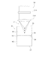
図1及び図2を用いて、レーザ加工装置1の全体構成を説明する。図1は、第1実施形態のレーザ加工装置の模式図である。図2は、空間光位相変調器の模式的動作説明図である。
1. First Embodiment (1) Overall Configuration The overall configuration of a laser processing apparatus 1 will be described with reference to FIGS. FIG. 1 is a schematic view of the laser processing apparatus according to the first embodiment. FIG. 2 is a schematic diagram illustrating the operation of the spatial light phase modulator.
レーザ加工装置1は、貼り合わせ基板W(以下、「基板W」)にスクライブラインを形成する装置である。基板Wは、第1基板W1と、第2基板W2とを有している。基板Wは、例えば、液晶ガラス基板である。
図2に示すように、第1基板W1と第2基板W2は、シール材40によって貼り合わされている。第1基板W1は外側面35と内側面36を有している。第2基板W2は外側面37と内側面38とを有している。内側面36と内側面38の間にシール材40が配置されている。
The laser processing apparatus 1 is an apparatus that forms a scribe line on a bonded substrate W (hereinafter, “substrate W”). The substrate W has a first substrate W1 and a second substrate W2. The substrate W is, for example, a liquid crystal glass substrate.
As shown in FIG. 2, the first substrate W1 and the second substrate W2 are bonded together by a
レーザ加工装置1は、第1レーザ装置3Aを有している。第1レーザ装置3Aは、第1基板W1に第1スクライブラインS1(図3、図4)を形成する装置である。 The laser processing device 1 has a first laser device 3A. The first laser device 3A is a device that forms a first scribe line S1 (FIGS. 3 and 4) on a first substrate W1.
第1レーザ装置3Aは、第1レーザ発振器15Aと、第1レーザ制御部17Aとを有している。第1レーザ発振器15Aは、例えば、波長340〜1100nmのピコ秒レーザである。第1レーザ制御部17Aは、第1レーザ発振器15Aの駆動及びレーザパワーを制御できる。
レーザ加工装置1は、第1伝送光学系5Aを有している。第1伝送光学系5Aは、第1レーザ装置3Aから出射されたレーザ光を変調する第1空間光位相変調器21Aを有している。第1空間光位相変調器21Aは、例えば透過型であり、透過型の空間光移送変調器(SLM:Spatial Light Modulator)であってもよい。また透過型の空間光移送変調器に代えて反射型液晶(LCOS:Liquid Crystal on Silicon)の空間光位相変調器などの反射型の空間光移送変調器を使用してもよい。第1空間光位相変調器21Aは、レーザ光を変調すると共に、下方に第1レーザ光L1を照射する。第1伝送光学系5Aは、第1空間光位相変調器21Aの下方に、第1集光レンズ23Aを有している。
The first laser device 3A has a
The laser processing device 1 has a first transmission
レーザ加工装置1は、第2レーザ装置3Bを備えている。第2レーザ装置3Bは、第2基板W2に第2スクライブラインS2(図3、図4)を形成する装置である。
第2レーザ装置3Bは、第2レーザ発振器15Bと、第2レーザ制御部17Bとを有している。第2レーザ発振器15Bは、例えば、波長340〜1100nmのピコ秒レーザである。第2レーザ制御部17Bは第2レーザ発振器15Bの駆動及びレーザパワーを制御できる。
レーザ加工装置1は、第2伝送光学系5Bを有している。第2伝送光学系5Bは、第2レーザ装置3Bから出射されたレーザ光を変調する第2空間光位相変調器21Bを有している。第2空間光位相変調器21Bは、第1空間光位相変調器21Aと同じく、SLMであってもよい。第2空間光位相変調器21Bは、レーザ光を変調すると共に、上方に第2レーザ光L2を照射する。第2伝送光学系5Bは、第2空間光位相変調器21Bの上方に、第2集光レンズ23Bを有している。
The laser processing device 1 includes a second laser device 3B. The second laser device 3B is a device that forms a second scribe line S2 (FIGS. 3 and 4) on the second substrate W2.
The second laser device 3B has a
The laser processing device 1 has a second transmission
レーザ加工装置1は、駆動部25を有している。駆動部25は、第1空間光位相変調器21A及び第2空間光位相変調器21Bにおける各画素電極に所定電圧を印加し、液晶層に所定の変調パターンを表示させ、これにより、レーザ光を第1空間光位相変調器21A及び第2空間光位相変調器21Bで所望に変調させる。ここで、液晶層に表示される変調パターンは、例えば、加工痕を形成しようとする位置、照射するレーザ光の波長、加工対象物の材料、及び第1伝送光学系5A及び第2伝送光学系5Bや加工対象物の屈折率等に基づいて予め導出され、制御部9に記憶されている。
この結果、図2に示すように、第1空間光位相変調器21A及び第2空間光位相変調器21Bは、任意の多数のビームを形成することができ、多数のビームによる同時加工が可能になる。
The laser processing device 1 has a
As a result, as shown in FIG. 2, the first spatial
レーザ加工装置1は、基板Wを保持して駆動する駆動装置7を有している。駆動装置7は、駆動装置操作部13によって移動される。駆動装置操作部13は、駆動装置7を水平方向に移動させる。
The laser processing device 1 has a
レーザ加工装置1は、制御部9を備えている。制御部9は、プロセッサ(例えば、CPU)と、記憶装置(例えば、ROM、RAM、HDD、SSDなど)と、各種インターフェース(例えば、A/Dコンバータ、D/Aコンバータ、通信インターフェースなど)を有するコンピュータシステムである。制御部9は、記憶部(記憶装置の記憶領域の一部又は全部に対応)に保存されたプログラムを実行することで、各種制御動作を行う。
制御部9は、単一のプロセッサで構成されていてもよいが、各制御のために独立した複数のプロセッサから構成されていてもよい。
The laser processing device 1 includes a
The
制御部9は、第1レーザ制御部17A及び第2レーザ制御部17Bを制御できる。制御部9は、駆動部25を制御できる。制御部9は、駆動装置操作部13を制御できる。
制御部9には、図示しないが、基板Wの大きさ、形状及び位置を検出するセンサ、各装置の状態を検出するためのセンサ及びスイッチ、並びに情報入力装置が接続されている。
The
Although not shown, a sensor for detecting the size, shape and position of the substrate W, sensors and switches for detecting the state of each device, and an information input device are connected to the
(2)スクライブ加工方法
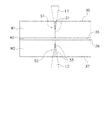
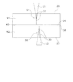
図3及び図4を用いて、レーザ加工装置1によるスクライブ加工方法を説明する。図3及び図4は、スクライブライン形成工程における基板の模式的断面である。
(2) Scribing Method A scribing method using the laser processing apparatus 1 will be described with reference to FIGS. 3 and 4 are schematic cross sections of the substrate in a scribe line forming step.
(2−1)ジャストカット加工
(a)第1レーザ光照射ステップ
第1基板W1側から第1レーザ光L1を照射することで、第1スクライブラインS1を形成する。具体的には、第1基板W1内部に光軸に沿って形成された複数の第1加工痕31が、平面方向に(紙面直交方向に)連続して形成される。第1加工痕31の厚み方向の形成位置は、第1基板W1の外側面35と内側面36との間である。
この実施形態では、第1スクライブラインのS1の平面視の1箇所では、複数の第1加工痕31は厚み方向に同時に形成される。
(2-1) Just Cut Processing (a) First Laser Light Irradiation Step The first scribe line S1 is formed by irradiating the first laser light L1 from the first substrate W1 side. Specifically, a plurality of first processing traces 31 formed along the optical axis inside the first substrate W1 are continuously formed in a plane direction (in a direction orthogonal to the paper surface). The formation position of the
In this embodiment, a plurality of first processing traces 31 are simultaneously formed in the thickness direction at one location of the first scribe line S1 in plan view.
(b)第2レーザ光照射ステップ
第2基板W2側から第2レーザ光L2を照射することで、第2スクライブラインS2を形成する。具体的には、図3に示すように、第2基板W2内部に光軸に沿って形成された複数の第2加工痕33が、第1加工痕31と一致する位置になるように、平面方向に(紙面直交方向に)連続して形成される。第2加工痕33の厚み方向の形成位置は、第2基板W2の内側面38と外側面37との間である。
この実施形態では、第2スクライブラインのS2の平面視の1箇所では、複数の第2加工痕33は厚み方向に同時に形成される。
(B) Second Laser Light Irradiation Step The second scribe line S2 is formed by irradiating the second laser light L2 from the second substrate W2 side. Specifically, as shown in FIG. 3, the plurality of second processing marks 33 formed along the optical axis inside the second substrate W <b> 2 are positioned on the plane so that the second processing marks 33 coincide with the first processing marks 31. It is formed continuously in the direction (in the direction perpendicular to the paper surface). The formation position of the
In this embodiment, at one location of the second scribe line S2 in plan view, the plurality of second processing marks 33 are formed simultaneously in the thickness direction.
(2−2)オフセットカット加工
(a)第1レーザ光照射ステップ
第1基板W1側から第1レーザ光L1を照射することで、第1スクライブラインS1を形成する。具体的には、第1基板W1内部に光軸に沿って形成された複数の第1加工痕31が、平面方向に(紙面直交方向に)連続して形成される。第1加工痕31の厚み方向の形成位置は、第1基板W1の外側面35と内側面36との間である。
(2-2) Offset cut processing (a) First laser light irradiation step The first scribe line S1 is formed by irradiating the first laser light L1 from the first substrate W1 side. Specifically, a plurality of first processing traces 31 formed along the optical axis inside the first substrate W1 are continuously formed in a plane direction (in a direction orthogonal to the paper surface). The formation position of the
(b)第2レーザ光照射ステップ
第2基板W2側から第2レーザ光L2を照射することで、第2スクライブラインS2を形成する。具体的には、図4に示すように、第2基板W2内部に光軸に沿って形成された複数の第2加工痕33が、第1加工痕31からずれた位置で平行になるように、平面方向に(紙面直交方向に)連続して形成される。第2加工痕33の厚み方向の形成位置は、第2基板W2の内側面38と外側面37との間である。
(B) Second Laser Light Irradiation Step The second scribe line S2 is formed by irradiating the second laser light L2 from the second substrate W2 side. Specifically, as shown in FIG. 4, the plurality of second processing marks 33 formed along the optical axis inside the second substrate W2 are parallel to each other at positions shifted from the first processing marks 31. Are formed continuously in the plane direction (in the direction perpendicular to the paper surface). The formation position of the
上記に説明したジャストカット加工とオフセット加工とを切り換えるときに、第2レーザ光照射ステップにおけるレーザ光照射位置がジャスト位置とオフセット位置とで変更される。具体的には、駆動部25が第2空間光位相変調器21Bを制御して、レーザ光照射位置を変更する。
この分断方法では、空間光位相変調を用いることで、第1スクライブラインS1と第2スクライブラインS2を一致させることと、ずらすこととを容易に切り換えられる。したがって、スクライブラインを加工する自由度が向上する。
When switching between the just-cut processing and the offset processing described above, the laser light irradiation position in the second laser light irradiation step is changed between the just position and the offset position. Specifically, the
In this dividing method, by using spatial light phase modulation, it is possible to easily switch between matching and shifting the first scribe line S1 and the second scribe line S2. Therefore, the degree of freedom in processing the scribe line is improved.
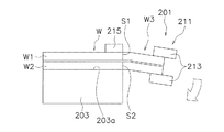
(3)基板分断装置
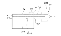
図5及び図6を用いて、基板分断装置201を説明する。図5及び図6は、基板分断装置の構成及び動作を説明する模式図である。なお、基板分断装置201は、レーザ加工装置1の制御部9によって制御されてもよいし、他の制御部によって制御されてもよい。
基板分断装置201は、スクライブラインが形成された基板から端材を分割除去することで製品を切り出す装置である。
(3) Board Cutting Apparatus The
The
基板分断装置201は、保持テーブル203を有している。保持テーブル203は、水平な吸着面203aを有しており、そこには加工対象となる基板Wが載置される。保持テーブル203の吸着面203aには、基板Wを安定保持する多数のエア吸着孔(図示せず)が設けられている。
保持テーブル203は、特に、基板Wの製品部分を吸着固定する吸着台である。第2スクライブラインS2が保持テーブル203の縁部に一致するように、基板Wは保持テーブル203に置かれる。
The
The holding table 203 is an adsorption table for adsorbing and fixing the product portion of the substrate W, in particular. The substrate W is placed on the holding table 203 such that the second scribe line S2 coincides with the edge of the holding table 203.
基板分断装置201は、チャック機構211を有している。チャック機構211は、保持テーブル203の吸着面203aからはみ出した基板Wの一端である端材W3を掴むように把持する装置である。
チャック機構211は、チャック部材213を有している。チャック部材213は、開閉自在に構成されている。
チャック機構211は、チャック部材213を駆動するための把持動作機構(図示せず)を有している。
基板分断装置201は、基板Wの製品部分(第1及び第2スクライブラインS1、S2を挟んで端材W3と反対側の部分)を上側から押さえて固定するための押圧機構215をさらに有している。
The
The
The
The
基板分断装置201は、回動機構(図示せず)を有している。回動機構は、チャック部材213が紙面直交方向に延びる軸を支点として所定角度だけ回動できるように、チャック部材213を保持している。回動機構は、例えば、回転モータを有している。
基板分断装置201は、昇降機構(図示せず)を有している。昇降機構は、チャック部材213及び回動機構を昇降させるための装置である。昇降機構は、例えば、圧力シリンダを有している。
The
The
基板分断装置201は、図5に示すように、チャック部材213によって端材W3を把持する。
次に、基板分断装置201は、図6に示すように、チャック部材213を傾けることで、端材W3を製品から切り離す。このとき、押圧機構215は、基板Wの製品部分を保持テーブル203との間で挟むことで、その部分を保持テーブル203から浮かないようにしている。
この結果、第1基板W1の第1スクライブラインS1と第2基板W2の第2スクライブラインS2に沿って、分断が行われる。
As shown in FIG. 5, the
Next, as shown in FIG. 6, the
As a result, the cutting is performed along the first scribe line S1 of the first substrate W1 and the second scribe line S2 of the second substrate W2.
2.他の実施形態
以上、本発明の一実施形態について説明したが、本発明は上記実施形態に限定されるものではなく、発明の要旨を逸脱しない範囲で種々の変更が可能である。特に、本明細書に書かれた複数の実施形態及び変形例は必要に応じて任意に組み合せ可能である。
基板は、ガラス、半導体ウェハ、セラミックス等の脆性材料基板であればよく、特に限定されない。
前記実施形態では基板分断装置は基板の端材を除去する装置であったが、他の基板分断装置であってもよい。
2. Other Embodiments An embodiment of the present invention has been described above, but the present invention is not limited to the above embodiment, and various changes can be made without departing from the gist of the invention. In particular, a plurality of embodiments and modifications described in this specification can be arbitrarily combined as needed.
The substrate is not particularly limited as long as it is a substrate made of a brittle material such as glass, a semiconductor wafer, and ceramics.
In the above-described embodiment, the substrate cutting device is a device for removing offcuts of the substrate, but may be another substrate cutting device.
本発明は、レーザ装置を用いたパルスによる基板の内部加工を平面方向に断続的に行うことでスクライブラインを形成する方法及び装置に広く適用できる。 INDUSTRIAL APPLICATION This invention can be widely applied to the method and apparatus which form a scribe line by performing internal processing of a board | substrate by the pulse using a laser apparatus intermittently in a plane direction.
1 :レーザ加工装置
3A :第1レーザ装置
3B :第2レーザ装置
5A :第1伝送光学系
5B :第2伝送光学系
7 :駆動装置
9 :制御部
13 :駆動装置操作部
15A :第1レーザ発振器
15B :第2レーザ発振器
17A :第1レーザ制御部
17B :第2レーザ制御部
21A :第1空間光位相変調器
21B :第2空間光位相変調器
25 :駆動部
S1 :第1スクライブライン
S2 :第2スクライブライン
W :貼り合わせ基板
W1 :第1基板
W2 :第2基板
W3 :端材
1: laser processing device 3A: first laser device 3B:
Claims (2)
前記第1基板に第1スクライブラインを形成する第1レーザ光照射ステップと、
空間光位相変調によって、前記第1基板の前記第1スクライブラインと平面視で同じ第1位置または異なる第2位置に、前記第2基板に第2スクライブラインを形成する第2レーザ光照射ステップと、
前記第2レーザ光照射ステップにおけるレーザ光照射位置を前記第1位置と前記第2位置とで変更する照射位置変更ステップと、
前記第1基板と前記第2基板に力を加えることで、前記第1スクライブラインと前記第2スクライブラインに沿ってそれぞれ前記第1基板と前記第2基板を分断する分断ステップと、
を備えている、貼り合わせ基板の分断方法。 A method for cutting a bonded substrate having a first substrate and a second substrate,
A first laser beam irradiation step of forming a first scribe line on the first substrate;
A second laser beam irradiation step of forming a second scribe line on the second substrate at the same first position or a different second position in plan view as the first scribe line of the first substrate by spatial light phase modulation; ,
An irradiation position changing step of changing a laser light irradiation position in the second laser light irradiation step between the first position and the second position;
A dividing step of dividing the first substrate and the second substrate along the first scribe line and the second scribe line by applying a force to the first substrate and the second substrate,
A method for cutting a bonded substrate, comprising:
前記第1基板に第1スクライブラインを形成する第1レーザ光照射ステップと;空間光位相変調によって、前記第1基板の前記第1スクライブラインと平面視で同じ第1位置または異なる第2位置に、前記第2基板に第2スクライブラインを形成する第2レーザ光照射ステップと;前記第2レーザ光照射ステップにおけるレーザ光照射位置を前記第1位置と前記第2位置とで変更する照射位置変更ステップと;を実行するレーザ装置と、
前記第1基板と前記第2基板に力を加えることで、前記第1スクライブラインと前記第2スクライブラインに沿ってそれぞれ前記第1基板と前記第2基板を分断する分断ステップを実行する基板分断装置と、
を備えた貼り合わせ基板の分断装置。 An apparatus for cutting a bonded substrate having a first substrate and a second substrate,
A first laser beam irradiating step for forming a first scribe line on the first substrate; and a second position different from the first scribe line on the first substrate in plan view by the spatial light phase modulation. A second laser light irradiation step of forming a second scribe line on the second substrate; and an irradiation position change for changing a laser light irradiation position in the second laser light irradiation step between the first position and the second position. A laser device for performing steps;
By applying a force to the first substrate and the second substrate, a substrate dividing step for performing a dividing step of dividing the first substrate and the second substrate along the first scribe line and the second scribe line, respectively. Equipment and
For cutting a bonded substrate.
Priority Applications (4)
| Application Number | Priority Date | Filing Date | Title |
|---|---|---|---|
| JP2018124059A JP2020004890A (en) | 2018-06-29 | 2018-06-29 | Method and apparatus for cutting bonded substrates |
| KR1020190075716A KR20200002633A (en) | 2018-06-29 | 2019-06-25 | Method and apparatus for dividing laminated substrate |
| TW108122485A TW202000357A (en) | 2018-06-29 | 2019-06-27 | Method and device for dividing laminated substrate to facilitate an operation of dividing the laminated substrate along the scribe line |
| CN201910567295.3A CN110722271A (en) | 2018-06-29 | 2019-06-27 | Method and apparatus for dividing bonded substrate |
Applications Claiming Priority (1)
| Application Number | Priority Date | Filing Date | Title |
|---|---|---|---|
| JP2018124059A JP2020004890A (en) | 2018-06-29 | 2018-06-29 | Method and apparatus for cutting bonded substrates |
Publications (1)
| Publication Number | Publication Date |
|---|---|
| JP2020004890A true JP2020004890A (en) | 2020-01-09 |
Family
ID=69100422
Family Applications (1)
| Application Number | Title | Priority Date | Filing Date |
|---|---|---|---|
| JP2018124059A Pending JP2020004890A (en) | 2018-06-29 | 2018-06-29 | Method and apparatus for cutting bonded substrates |
Country Status (1)
| Country | Link |
|---|---|
| JP (1) | JP2020004890A (en) |
Cited By (1)
| Publication number | Priority date | Publication date | Assignee | Title |
|---|---|---|---|---|
| JPWO2022186188A1 (en) * | 2021-03-02 | 2022-09-09 |
-
2018
- 2018-06-29 JP JP2018124059A patent/JP2020004890A/en active Pending
Cited By (1)
| Publication number | Priority date | Publication date | Assignee | Title |
|---|---|---|---|---|
| JPWO2022186188A1 (en) * | 2021-03-02 | 2022-09-09 |
Similar Documents
| Publication | Publication Date | Title |
|---|---|---|
| JP2020004889A (en) | Substrate cutting method and substrate cutting device | |
| TW498006B (en) | Laser cutting method, laser cutting apparatus, and method and apparatus for manufacturing liquid crystal device | |
| US10322526B2 (en) | Laser processing method | |
| TWI413565B (en) | Method of cutting substrate | |
| CN110722271A (en) | Method and apparatus for dividing bonded substrate | |
| JP5398332B2 (en) | Method and apparatus for manufacturing semiconductor wafer | |
| WO2007125799A1 (en) | Laser processing method and laser processing apparatus | |
| TWI862553B (en) | Composite material cutting method | |
| WO2015182558A1 (en) | Method for manufacturing glass substrate and electronic device | |
| JP2020004890A (en) | Method and apparatus for cutting bonded substrates | |
| JP2002293560A5 (en) | ||
| JP2005338281A (en) | Thin film device manufacturing method and glass substrate bonding method | |
| JP2020001072A (en) | Method and apparatus for cutting bonded substrates | |
| CN103842305B (en) | The laser processing device of glass substrate | |
| JP2020082153A (en) | Laser processing device | |
| JP2009190943A (en) | Substrate cutting apparatus, substrate cutting method, and substrate manufactured using the method | |
| KR102633196B1 (en) | Scribing apparatus and scribing method | |
| JP2020164358A (en) | Partial punching method and partial punching device for laminated substrate | |
| JP2019139182A (en) | Method for producing liquid crystal panel | |
| CN111230312A (en) | Laser processing apparatus | |
| CN107953034A (en) | The processing method of adhesive substrates | |
| JP2020001081A (en) | Laser processing method of substrate, and laser processing device | |
| CN111230313A (en) | Laser processing apparatus | |
| JP2020082154A (en) | Laser processing device | |
| JPWO2019131525A1 (en) | Scribe processing method and scribe processing equipment |