JP2020004983A - フレキシブルプリント配線板 - Google Patents
フレキシブルプリント配線板 Download PDFInfo
- Publication number
- JP2020004983A JP2020004983A JP2019146277A JP2019146277A JP2020004983A JP 2020004983 A JP2020004983 A JP 2020004983A JP 2019146277 A JP2019146277 A JP 2019146277A JP 2019146277 A JP2019146277 A JP 2019146277A JP 2020004983 A JP2020004983 A JP 2020004983A
- Authority
- JP
- Japan
- Prior art keywords
- fuse
- fuse portion
- flexible printed
- wiring board
- printed wiring
- Prior art date
- Legal status (The legal status is an assumption and is not a legal conclusion. Google has not performed a legal analysis and makes no representation as to the accuracy of the status listed.)
- Granted
Links
Images

Classifications
-
- H—ELECTRICITY
- H05—ELECTRIC TECHNIQUES NOT OTHERWISE PROVIDED FOR
- H05K—PRINTED CIRCUITS; CASINGS OR CONSTRUCTIONAL DETAILS OF ELECTRIC APPARATUS; MANUFACTURE OF ASSEMBLAGES OF ELECTRICAL COMPONENTS
- H05K1/00—Printed circuits
- H05K1/02—Details
- H05K1/0286—Programmable, customizable or modifiable circuits
- H05K1/0293—Individual printed conductors which are adapted for modification, e.g. fusable or breakable conductors, printed switches
-
- H—ELECTRICITY
- H01—ELECTRIC ELEMENTS
- H01H—ELECTRIC SWITCHES; RELAYS; SELECTORS; EMERGENCY PROTECTIVE DEVICES
- H01H85/00—Protective devices in which the current flows through a part of fusible material and this current is interrupted by displacement of the fusible material when this current becomes excessive
- H01H85/02—Details
- H01H85/0241—Structural association of a fuse and another component or apparatus
-
- H—ELECTRICITY
- H01—ELECTRIC ELEMENTS
- H01H—ELECTRIC SWITCHES; RELAYS; SELECTORS; EMERGENCY PROTECTIVE DEVICES
- H01H85/00—Protective devices in which the current flows through a part of fusible material and this current is interrupted by displacement of the fusible material when this current becomes excessive
- H01H85/02—Details
- H01H85/04—Fuses, i.e. expendable parts of the protective device, e.g. cartridges
- H01H85/041—Fuses, i.e. expendable parts of the protective device, e.g. cartridges characterised by the type
- H01H85/046—Fuses formed as printed circuits
-
- H—ELECTRICITY
- H05—ELECTRIC TECHNIQUES NOT OTHERWISE PROVIDED FOR
- H05K—PRINTED CIRCUITS; CASINGS OR CONSTRUCTIONAL DETAILS OF ELECTRIC APPARATUS; MANUFACTURE OF ASSEMBLAGES OF ELECTRICAL COMPONENTS
- H05K1/00—Printed circuits
- H05K1/02—Details
- H05K1/0213—Electrical arrangements not otherwise provided for
- H05K1/0254—High voltage adaptations; Electrical insulation details; Overvoltage or electrostatic discharge protection ; Arrangements for regulating voltages or for using plural voltages
- H05K1/0257—Overvoltage protection
-
- H—ELECTRICITY
- H05—ELECTRIC TECHNIQUES NOT OTHERWISE PROVIDED FOR
- H05K—PRINTED CIRCUITS; CASINGS OR CONSTRUCTIONAL DETAILS OF ELECTRIC APPARATUS; MANUFACTURE OF ASSEMBLAGES OF ELECTRICAL COMPONENTS
- H05K1/00—Printed circuits
- H05K1/02—Details
- H05K1/0277—Bendability or stretchability details
- H05K1/028—Bending or folding regions of flexible printed circuits
-
- H—ELECTRICITY
- H01—ELECTRIC ELEMENTS
- H01H—ELECTRIC SWITCHES; RELAYS; SELECTORS; EMERGENCY PROTECTIVE DEVICES
- H01H85/00—Protective devices in which the current flows through a part of fusible material and this current is interrupted by displacement of the fusible material when this current becomes excessive
- H01H85/02—Details
- H01H85/0241—Structural association of a fuse and another component or apparatus
- H01H2085/0275—Structural association with a printed circuit board
-
- H—ELECTRICITY
- H01—ELECTRIC ELEMENTS
- H01H—ELECTRIC SWITCHES; RELAYS; SELECTORS; EMERGENCY PROTECTIVE DEVICES
- H01H69/00—Apparatus or processes for the manufacture of emergency protective devices
- H01H69/02—Manufacture of fuses
- H01H69/022—Manufacture of fuses of printed circuit fuses
-
- H—ELECTRICITY
- H01—ELECTRIC ELEMENTS
- H01H—ELECTRIC SWITCHES; RELAYS; SELECTORS; EMERGENCY PROTECTIVE DEVICES
- H01H85/00—Protective devices in which the current flows through a part of fusible material and this current is interrupted by displacement of the fusible material when this current becomes excessive
- H01H85/02—Details
- H01H85/04—Fuses, i.e. expendable parts of the protective device, e.g. cartridges
- H01H85/05—Component parts thereof
- H01H85/055—Fusible members
- H01H85/08—Fusible members characterised by the shape or form of the fusible member
- H01H85/10—Fusible members characterised by the shape or form of the fusible member with constriction for localised fusing
-
- H—ELECTRICITY
- H05—ELECTRIC TECHNIQUES NOT OTHERWISE PROVIDED FOR
- H05K—PRINTED CIRCUITS; CASINGS OR CONSTRUCTIONAL DETAILS OF ELECTRIC APPARATUS; MANUFACTURE OF ASSEMBLAGES OF ELECTRICAL COMPONENTS
- H05K1/00—Printed circuits
- H05K1/02—Details
- H05K1/0213—Electrical arrangements not otherwise provided for
- H05K1/0254—High voltage adaptations; Electrical insulation details; Overvoltage or electrostatic discharge protection ; Arrangements for regulating voltages or for using plural voltages
- H05K1/0256—Electrical insulation details, e.g. around high voltage areas
-
- H—ELECTRICITY
- H05—ELECTRIC TECHNIQUES NOT OTHERWISE PROVIDED FOR
- H05K—PRINTED CIRCUITS; CASINGS OR CONSTRUCTIONAL DETAILS OF ELECTRIC APPARATUS; MANUFACTURE OF ASSEMBLAGES OF ELECTRICAL COMPONENTS
- H05K1/00—Printed circuits
- H05K1/02—Details
- H05K1/03—Use of materials for the substrate
- H05K1/0393—Flexible materials
-
- H—ELECTRICITY
- H05—ELECTRIC TECHNIQUES NOT OTHERWISE PROVIDED FOR
- H05K—PRINTED CIRCUITS; CASINGS OR CONSTRUCTIONAL DETAILS OF ELECTRIC APPARATUS; MANUFACTURE OF ASSEMBLAGES OF ELECTRICAL COMPONENTS
- H05K2201/00—Indexing scheme relating to printed circuits covered by H05K1/00
- H05K2201/09—Shape and layout
- H05K2201/09009—Substrate related
- H05K2201/09063—Holes or slots in insulating substrate not used for electrical connections
-
- H—ELECTRICITY
- H05—ELECTRIC TECHNIQUES NOT OTHERWISE PROVIDED FOR
- H05K—PRINTED CIRCUITS; CASINGS OR CONSTRUCTIONAL DETAILS OF ELECTRIC APPARATUS; MANUFACTURE OF ASSEMBLAGES OF ELECTRICAL COMPONENTS
- H05K2201/00—Indexing scheme relating to printed circuits covered by H05K1/00
- H05K2201/09—Shape and layout
- H05K2201/09209—Shape and layout details of conductors
- H05K2201/09654—Shape and layout details of conductors covering at least two types of conductors provided for in H05K2201/09218 - H05K2201/095
- H05K2201/09727—Varying width along a single conductor; Conductors or pads having different widths
-
- H—ELECTRICITY
- H05—ELECTRIC TECHNIQUES NOT OTHERWISE PROVIDED FOR
- H05K—PRINTED CIRCUITS; CASINGS OR CONSTRUCTIONAL DETAILS OF ELECTRIC APPARATUS; MANUFACTURE OF ASSEMBLAGES OF ELECTRICAL COMPONENTS
- H05K2201/00—Indexing scheme relating to printed circuits covered by H05K1/00
- H05K2201/10—Details of components or other objects attached to or integrated in a printed circuit board
- H05K2201/10007—Types of components
- H05K2201/10181—Fuse
-
- H—ELECTRICITY
- H05—ELECTRIC TECHNIQUES NOT OTHERWISE PROVIDED FOR
- H05K—PRINTED CIRCUITS; CASINGS OR CONSTRUCTIONAL DETAILS OF ELECTRIC APPARATUS; MANUFACTURE OF ASSEMBLAGES OF ELECTRICAL COMPONENTS
- H05K2203/00—Indexing scheme relating to apparatus or processes for manufacturing printed circuits covered by H05K3/00
- H05K2203/06—Lamination
- H05K2203/068—Features of the lamination press or of the lamination process, e.g. using special separator sheets
-
- H—ELECTRICITY
- H05—ELECTRIC TECHNIQUES NOT OTHERWISE PROVIDED FOR
- H05K—PRINTED CIRCUITS; CASINGS OR CONSTRUCTIONAL DETAILS OF ELECTRIC APPARATUS; MANUFACTURE OF ASSEMBLAGES OF ELECTRICAL COMPONENTS
- H05K2203/00—Indexing scheme relating to apparatus or processes for manufacturing printed circuits covered by H05K3/00
- H05K2203/10—Using electric, magnetic and electromagnetic fields; Using laser light
- H05K2203/107—Using laser light
-
- H—ELECTRICITY
- H05—ELECTRIC TECHNIQUES NOT OTHERWISE PROVIDED FOR
- H05K—PRINTED CIRCUITS; CASINGS OR CONSTRUCTIONAL DETAILS OF ELECTRIC APPARATUS; MANUFACTURE OF ASSEMBLAGES OF ELECTRICAL COMPONENTS
- H05K3/00—Apparatus or processes for manufacturing printed circuits
- H05K3/0011—Working of insulating substrates or insulating layers
- H05K3/0017—Etching of the substrate by chemical or physical means
- H05K3/0026—Etching of the substrate by chemical or physical means by laser ablation
-
- H—ELECTRICITY
- H05—ELECTRIC TECHNIQUES NOT OTHERWISE PROVIDED FOR
- H05K—PRINTED CIRCUITS; CASINGS OR CONSTRUCTIONAL DETAILS OF ELECTRIC APPARATUS; MANUFACTURE OF ASSEMBLAGES OF ELECTRICAL COMPONENTS
- H05K3/00—Apparatus or processes for manufacturing printed circuits
- H05K3/0011—Working of insulating substrates or insulating layers
- H05K3/0044—Mechanical working of the substrate, e.g. drilling or punching
- H05K3/005—Punching of holes
-
- H—ELECTRICITY
- H05—ELECTRIC TECHNIQUES NOT OTHERWISE PROVIDED FOR
- H05K—PRINTED CIRCUITS; CASINGS OR CONSTRUCTIONAL DETAILS OF ELECTRIC APPARATUS; MANUFACTURE OF ASSEMBLAGES OF ELECTRICAL COMPONENTS
- H05K3/00—Apparatus or processes for manufacturing printed circuits
- H05K3/02—Apparatus or processes for manufacturing printed circuits in which the conductive material is applied to the surface of the insulating support and is thereafter removed from such areas of the surface which are not intended for current conducting or shielding
- H05K3/027—Apparatus or processes for manufacturing printed circuits in which the conductive material is applied to the surface of the insulating support and is thereafter removed from such areas of the surface which are not intended for current conducting or shielding the conductive material being removed by irradiation, e.g. by photons, alpha or beta particles
-
- H—ELECTRICITY
- H05—ELECTRIC TECHNIQUES NOT OTHERWISE PROVIDED FOR
- H05K—PRINTED CIRCUITS; CASINGS OR CONSTRUCTIONAL DETAILS OF ELECTRIC APPARATUS; MANUFACTURE OF ASSEMBLAGES OF ELECTRICAL COMPONENTS
- H05K3/00—Apparatus or processes for manufacturing printed circuits
- H05K3/02—Apparatus or processes for manufacturing printed circuits in which the conductive material is applied to the surface of the insulating support and is thereafter removed from such areas of the surface which are not intended for current conducting or shielding
- H05K3/06—Apparatus or processes for manufacturing printed circuits in which the conductive material is applied to the surface of the insulating support and is thereafter removed from such areas of the surface which are not intended for current conducting or shielding the conductive material being removed chemically or electrolytically, e.g. by photo-etch process
- H05K3/061—Etching masks
- H05K3/064—Photoresists
Landscapes
- Engineering & Computer Science (AREA)
- Microelectronics & Electronic Packaging (AREA)
- Power Engineering (AREA)
- Parts Printed On Printed Circuit Boards (AREA)
- Structure Of Printed Boards (AREA)
- Fuses (AREA)
- Manufacturing & Machinery (AREA)
- Thermistors And Varistors (AREA)
Abstract
Description
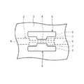
本発明の一態様に係るフレキシブルプリント配線板は、絶縁性を有するベースフィルムと、このベースフィルムの一方の面側に積層される導電パターンとを備え、この導電パターンが、回路の一部を構成し、他の部分より断面積が小さい1又は複数のヒューズ部を有するフレキシブルプリント配線板であって、平面視で上記ヒューズ部の左右両側のうち少なくとも一方側に表裏に貫通する1又は複数の開口部を備える。
以下、本発明に係るフレキシブルプリント配線板の実施形態について図面を参照しつつ詳説する。
図1及び2に示す本発明の一実施形態のフレキシブルプリント配線板は、絶縁性を有するベースフィルム1と、このベースフィルム1の一方の面側に積層される導電パターン2とを備える。また、当該フレキシブルプリント配線板は、ベースフィルム1及び導電パターン2の一方の面側を覆うよう積層される絶縁層3を備える。
ベースフィルム1は、導電パターン2を支持する部材であって、当該フレキシブルプリント配線板の強度を担保する構造材である。
導電パターン2は、層状の導体を少なくとも部分的に回路を構成するようパターニングして形成される。この導電パターン2は、電路となる配線部6と、この配線部6の一部分の幅を減じることにより他の部分よりも断面積を小さくしたヒューズ部4とを有する。また、導電パターン2は、図示しないが、例えば電子部品の実装のためのランド、配線接続のため端子部等を有してもよい。
絶縁層3は、ベースフィルム1及び導電パターン2を含む積層体の一方の面側に被覆されている。この絶縁層3は、主に導電パターン2が他の部材等と接触して損傷することや短絡することを防止する。
ヒューズ部4は、配線部6の一部分の幅を減じることにより、配線部6の他の部分よりも断面積が小さいことで単位長さあたりの電気抵抗が大きく、過電流が流れるとジュール熱により加熱して溶断するよう形成されている。つまり、ヒューズ部4は、前後の回路部より線幅が小さく形成されている。
一対の開口部5は、平面視でヒューズ部4を流れる電流の向きに垂直な方向でヒューズ部4の両側に形成されている。また、一対の開口部5は、ヒューズ部4の長さ方向の中心を軸として左右対称に形成されている。また、開口部5は、当該フレキシブルプリント配線板が応力集中によって破断し易くなることを避けるために、角部を面取りした形状とすることが好ましい。
当該フレキシブルプリント配線板は、ベースフィルム1の一方の面側に積層した導体層のパターニングによりヒューズ部4を有する導電パターン2を形成する工程と、ベースフィルム1及び導電パターン2の積層体の一方の面側に絶縁層3を積層する工程と、ベースフィルム1、導電パターン2及び絶縁層3の積層体に開口部を形成する工程とを備える方法によって製造することができる。
上記導電パターン形成工程では、例えばフォトリソグラフィによりレジストパターンを形成して導体層をエッチングする公知の方法を用いることができる。なお、ベースフィルム1と導電パターン2を形成する導体層との積層は、接着剤を用いる方法、熱圧着する方法、ベースフィルム1上に例えば蒸着、メッキ等によって導体層を積層する方法などを用いることができる。
上記絶縁層積層工程では、絶縁層3として、例えば絶縁フィルムの裏面に接着剤層を有するカバーレイをベースフィルム1及び導電パターン2の積層体の一方の面側に積層する。ヒューズ部4の両側においてベースフィルム1と絶縁層3とを確実に接着するために、真空熱圧着装置等を用いることが好ましい。
上記開口部形成工程では、例えばパンチ及びダイを用いる打ち抜きや、レーザー加工等により、ヒューズ部4の両側に開口部5を形成する。
上述のように、当該フレキシブルプリント配線板は、複数の開口部5を備えることによって、ベースフィルム1及び絶縁層3のヒューズ部4から熱が伝導し得る近傍領域の体積、ひいては熱容量を低減し、ヒューズ部4からの放熱による電流遮断の遅れを低減する。これにより、ベースフィルム1及び絶縁層3に伝達される熱量を低減し、過電流を比較的確実に遮断することができる。
今回開示された実施の形態は全ての点で例示であって制限的なものではないと考えられるべきである。本発明の範囲は、上記実施形態の構成に限定されるものではなく、特許請求の範囲によって示され、特許請求の範囲と均等の意味及び範囲内での全ての変更が含まれることが意図される。
2 導電パターン
3 絶縁層
4 ヒューズ部
5 開口部
6 配線部
7 凸部
8 基部
Claims (6)
- 絶縁性を有するベースフィルムと、
前記ベースフィルムの一方の面側に積層される導電パターンと、
前記ベースフィルム及び前記導電パターンの前記一方の面側を覆うように積層される絶縁層と、を備え、
前記導電パターンが、回路の一部を構成し、他の部分より断面積が小さい1又は複数のヒューズ部を有するフレキシブルプリント配線板であって、
平面視で前記ヒューズ部の左右両側のうち少なくとも一方側に表裏に貫通する1又は複数の開口部を備え、
前記ヒューズ部の側縁から前記開口部までの間隔が最短の部分が、平面視で前記ヒューズ部の側縁のうち中央領域にのみ配されているフレキシブルプリント配線板。 - 平面視で前記ヒューズ部の側縁のうち前記中央領域にのみ前記開口部を備える請求項1に記載のフレキシブルプリント配線板。
- 前記ヒューズ部の長さ方向両端からそれぞれ前記ヒューズ部の全長の30%を除く領域にのみ前記開口部を有する請求項1または請求項2に記載のフレキシブルプリント配線板。
- 前記開口部と前記ヒューズ部との間に、前記ベースフィルムと前記絶縁層との積層構造を有する請求項1から請求項3のいずれか1項に記載のフレキシブルプリント配線板。
- 前記ヒューズ部の側縁から前記開口部までの間隔が最短の部分が、前記ヒューズ部の側縁と平行である請求項1から請求項4のいずれか1項に記載のフレキシブルプリント配線板。
- 前記ヒューズ部の線幅は、前記導電パターンのうち前記ヒューズ部の両端と接続された部分よりも小さくされており、
前記ヒューズ部の側縁から前記開口部までの間隔が最短の部分は、平面視で、前記ヒューズ部の両端と接続された前記導電パターンの側縁を結ぶ線よりも前記ヒューズ部側に入り込んでいる請求項1から請求項5のいずれか1項に記載のフレキシブルプリント配線板。
Priority Applications (1)
| Application Number | Priority Date | Filing Date | Title |
|---|---|---|---|
| JP2020086589A JP6950039B2 (ja) | 2015-06-24 | 2020-05-18 | フレキシブルプリント配線板 |
Applications Claiming Priority (2)
| Application Number | Priority Date | Filing Date | Title |
|---|---|---|---|
| JP2015127097 | 2015-06-24 | ||
| JP2015127097 | 2015-06-24 |
Related Parent Applications (1)
| Application Number | Title | Priority Date | Filing Date |
|---|---|---|---|
| JP2015208436A Division JP2017011253A (ja) | 2015-06-24 | 2015-10-22 | フレキシブルプリント配線板 |
Related Child Applications (1)
| Application Number | Title | Priority Date | Filing Date |
|---|---|---|---|
| JP2020086589A Division JP6950039B2 (ja) | 2015-06-24 | 2020-05-18 | フレキシブルプリント配線板 |
Publications (2)
| Publication Number | Publication Date |
|---|---|
| JP2020004983A true JP2020004983A (ja) | 2020-01-09 |
| JP6839238B2 JP6839238B2 (ja) | 2021-03-03 |
Family
ID=57764499
Family Applications (3)
| Application Number | Title | Priority Date | Filing Date |
|---|---|---|---|
| JP2015208436A Pending JP2017011253A (ja) | 2015-06-24 | 2015-10-22 | フレキシブルプリント配線板 |
| JP2019146277A Active JP6839238B2 (ja) | 2015-06-24 | 2019-08-08 | フレキシブルプリント配線板 |
| JP2020086589A Active JP6950039B2 (ja) | 2015-06-24 | 2020-05-18 | フレキシブルプリント配線板 |
Family Applications Before (1)
| Application Number | Title | Priority Date | Filing Date |
|---|---|---|---|
| JP2015208436A Pending JP2017011253A (ja) | 2015-06-24 | 2015-10-22 | フレキシブルプリント配線板 |
Family Applications After (1)
| Application Number | Title | Priority Date | Filing Date |
|---|---|---|---|
| JP2020086589A Active JP6950039B2 (ja) | 2015-06-24 | 2020-05-18 | フレキシブルプリント配線板 |
Country Status (3)
| Country | Link |
|---|---|
| US (1) | US10653007B2 (ja) |
| JP (3) | JP2017011253A (ja) |
| CN (1) | CN107710884B (ja) |
Families Citing this family (9)
| Publication number | Priority date | Publication date | Assignee | Title |
|---|---|---|---|---|
| DE102016220058A1 (de) * | 2016-10-14 | 2018-04-19 | Continental Automotive Gmbh | Schaltungsanordnung mit einer Schmelzsicherung, Kraftfahrzeug und Verfahren zum Herstellen der Schaltungsanordnung |
| CN108288573B (zh) * | 2018-03-13 | 2020-05-19 | 俞东 | Pcb基体熔断器 |
| US12294114B2 (en) * | 2018-07-10 | 2025-05-06 | Sanyo Electric Co., Ltd. | Flexible flat cable including protective element in middle of conductive wire covered by insulating sheet, battery module having the same, and method for manufacturing the same |
| DE202019103280U1 (de) * | 2019-06-12 | 2020-09-16 | Tridonic Gmbh & Co Kg | Leiterplatte mit innerer Leiterbahnsicherung |
| JP7025376B2 (ja) | 2019-06-17 | 2022-02-24 | 矢崎総業株式会社 | バスバモジュール |
| JP6887696B2 (ja) * | 2019-11-12 | 2021-06-16 | ジンヨングローバル カンパニーリミテッド | ヒューズ素子、フレキシブル配線基板及びバッテリーパック |
| JP7564995B2 (ja) | 2021-02-22 | 2024-10-10 | 株式会社オートネットワーク技術研究所 | 配線モジュール |
| JP7501425B2 (ja) * | 2021-03-30 | 2024-06-18 | 株式会社オートネットワーク技術研究所 | ヒューズ素子 |
| JP7629801B2 (ja) * | 2021-05-20 | 2025-02-14 | メクテック株式会社 | プリント基板 |
Citations (13)
| Publication number | Priority date | Publication date | Assignee | Title |
|---|---|---|---|---|
| JPS5314125U (ja) * | 1976-07-19 | 1978-02-06 | ||
| JPS5388193A (en) * | 1977-01-12 | 1978-08-03 | Philips Nv | Supporting body having pattern of electroconductive fine filament |
| JPS55108777U (ja) * | 1979-01-24 | 1980-07-30 | ||
| JPS55120063U (ja) * | 1979-02-19 | 1980-08-25 | ||
| JPS55152078U (ja) * | 1979-04-16 | 1980-11-01 | ||
| JPS58134853U (ja) * | 1982-03-08 | 1983-09-10 | マツダ株式会社 | プリント配線フユ−ズ |
| JPS633174U (ja) * | 1986-06-24 | 1988-01-11 | ||
| JPH05159691A (ja) * | 1991-12-02 | 1993-06-25 | Okaya Electric Ind Co Ltd | ヒューズ抵抗器の最小遮断電流調整方法 |
| EP1045625A1 (en) * | 1999-04-14 | 2000-10-18 | Helvar Oy Ab | A foil fuse made on a circuit board |
| WO2001059799A1 (de) * | 2000-02-10 | 2001-08-16 | Vosslon-Schwabe Electronik Gmbh | Leiterplattensicherung mit erhöhter sicherheit |
| JP2003173730A (ja) * | 2001-12-06 | 2003-06-20 | Tama Electric Co Ltd | ヒューズ抵抗 |
| EP2429267A1 (de) * | 2010-09-08 | 2012-03-14 | Vossloh-Schwabe Deutschland GmbH | Mehrlagige Leiterplatte mit Leiterplattensicherung |
| JP2012164758A (ja) * | 2011-02-04 | 2012-08-30 | Denso Corp | 電子制御装置 |
Family Cites Families (13)
| Publication number | Priority date | Publication date | Assignee | Title |
|---|---|---|---|---|
| JPS53109058U (ja) * | 1977-02-08 | 1978-09-01 | ||
| FR2394711A1 (fr) * | 1977-03-04 | 1979-01-12 | Glaenzer Spicer Sa | Perfectionnements aux joints homocinetiques de type " tripode " |
| US4296398A (en) * | 1978-12-18 | 1981-10-20 | Mcgalliard James D | Printed circuit fuse assembly |
| US4203781A (en) * | 1978-12-27 | 1980-05-20 | Bell Telephone Laboratories, Incorporated | Laser deformation of semiconductor junctions |
| JPS55103979U (ja) * | 1979-01-12 | 1980-07-19 | ||
| JPS55108776U (ja) * | 1979-01-24 | 1980-07-30 | ||
| JPS55168951U (ja) * | 1979-05-18 | 1980-12-04 | ||
| JPS58134853A (ja) * | 1982-01-28 | 1983-08-11 | 東洋製罐株式会社 | 側面継目を有する容器及びその製法 |
| US5196819A (en) * | 1991-02-28 | 1993-03-23 | Rock Ltd. Partnership | Printed circuits containing fuse elements and the method of making this circuit |
| US5923239A (en) * | 1997-12-02 | 1999-07-13 | Littelfuse, Inc. | Printed circuit board assembly having an integrated fusible link |
| JP2007317990A (ja) * | 2006-05-29 | 2007-12-06 | Fujikura Ltd | フレキシブルプリント配線板 |
| US7663204B2 (en) * | 2007-04-27 | 2010-02-16 | Powertech Technology Inc. | Substrate for multi-chip stacking, multi-chip stack package utilizing the substrate and its applications |
| US8971006B2 (en) | 2011-02-04 | 2015-03-03 | Denso Corporation | Electronic control device including interrupt wire |
-
2015
- 2015-10-22 JP JP2015208436A patent/JP2017011253A/ja active Pending
-
2016
- 2016-06-22 CN CN201680036855.7A patent/CN107710884B/zh active Active
- 2016-06-22 US US15/738,301 patent/US10653007B2/en active Active
-
2019
- 2019-08-08 JP JP2019146277A patent/JP6839238B2/ja active Active
-
2020
- 2020-05-18 JP JP2020086589A patent/JP6950039B2/ja active Active
Patent Citations (13)
| Publication number | Priority date | Publication date | Assignee | Title |
|---|---|---|---|---|
| JPS5314125U (ja) * | 1976-07-19 | 1978-02-06 | ||
| JPS5388193A (en) * | 1977-01-12 | 1978-08-03 | Philips Nv | Supporting body having pattern of electroconductive fine filament |
| JPS55108777U (ja) * | 1979-01-24 | 1980-07-30 | ||
| JPS55120063U (ja) * | 1979-02-19 | 1980-08-25 | ||
| JPS55152078U (ja) * | 1979-04-16 | 1980-11-01 | ||
| JPS58134853U (ja) * | 1982-03-08 | 1983-09-10 | マツダ株式会社 | プリント配線フユ−ズ |
| JPS633174U (ja) * | 1986-06-24 | 1988-01-11 | ||
| JPH05159691A (ja) * | 1991-12-02 | 1993-06-25 | Okaya Electric Ind Co Ltd | ヒューズ抵抗器の最小遮断電流調整方法 |
| EP1045625A1 (en) * | 1999-04-14 | 2000-10-18 | Helvar Oy Ab | A foil fuse made on a circuit board |
| WO2001059799A1 (de) * | 2000-02-10 | 2001-08-16 | Vosslon-Schwabe Electronik Gmbh | Leiterplattensicherung mit erhöhter sicherheit |
| JP2003173730A (ja) * | 2001-12-06 | 2003-06-20 | Tama Electric Co Ltd | ヒューズ抵抗 |
| EP2429267A1 (de) * | 2010-09-08 | 2012-03-14 | Vossloh-Schwabe Deutschland GmbH | Mehrlagige Leiterplatte mit Leiterplattensicherung |
| JP2012164758A (ja) * | 2011-02-04 | 2012-08-30 | Denso Corp | 電子制御装置 |
Also Published As
| Publication number | Publication date |
|---|---|
| US10653007B2 (en) | 2020-05-12 |
| JP6839238B2 (ja) | 2021-03-03 |
| CN107710884B (zh) | 2021-01-01 |
| CN107710884A (zh) | 2018-02-16 |
| JP6950039B2 (ja) | 2021-10-13 |
| US20180192511A1 (en) | 2018-07-05 |
| JP2020120140A (ja) | 2020-08-06 |
| JP2017011253A (ja) | 2017-01-12 |
Similar Documents
| Publication | Publication Date | Title |
|---|---|---|
| JP6950039B2 (ja) | フレキシブルプリント配線板 | |
| KR102254469B1 (ko) | 전력 전자 회로의 냉각 | |
| JP6453720B2 (ja) | フレキシブルプリント配線板 | |
| JP2017204525A (ja) | フレキシブルプリント配線板及び電子部品 | |
| JP6659253B2 (ja) | フレキシブルプリント配線板及びフレキシブルプリント配線板の製造方法 | |
| TW200911064A (en) | Connection structure between printed circuit board and electronic component | |
| US9852868B2 (en) | Chip fuse and manufacturing method therefor | |
| WO2018028213A1 (zh) | 一种含多功能铝箔的led灯带线路板模组及制造方法 | |
| CN108353499B (zh) | 基板及基板的制造方法 | |
| US9801283B2 (en) | Method of producing electronic components | |
| JP2015035281A (ja) | 保護素子、及びこれを用いた保護回路基板 | |
| KR20150037306A (ko) | 경연성 인쇄회로기판 | |
| JP6231324B2 (ja) | 保護回路基板 | |
| US9142949B2 (en) | PTC device | |
| US20170086297A1 (en) | Electronic device | |
| JP5672381B2 (ja) | 多層配線板 | |
| WO2016208613A1 (ja) | フレキシブルプリント配線板 | |
| CN108353508A (zh) | 基板及基板的制造方法 | |
| CN104658726A (zh) | 过电流保护元件及其保护电路板 | |
| JP2015002033A (ja) | フラットケーブルおよびその製造方法 | |
| JP2018207082A (ja) | リジッドフレキシブル配線板およびその製造方法 | |
| JP2022178360A (ja) | プリント基板 | |
| WO2017109882A1 (ja) | 基板及び基板の製造方法 | |
| JP6617505B2 (ja) | フラットケーブル接続構造体 | |
| US20130314201A1 (en) | Over-current protection fuses |
Legal Events
| Date | Code | Title | Description |
|---|---|---|---|
| A621 | Written request for application examination |
Free format text: JAPANESE INTERMEDIATE CODE: A621 Effective date: 20190808 |
|
| A871 | Explanation of circumstances concerning accelerated examination |
Free format text: JAPANESE INTERMEDIATE CODE: A871 Effective date: 20190808 |
|
| A975 | Report on accelerated examination |
Free format text: JAPANESE INTERMEDIATE CODE: A971005 Effective date: 20191205 |
|
| A131 | Notification of reasons for refusal |
Free format text: JAPANESE INTERMEDIATE CODE: A131 Effective date: 20191210 |
|
| A521 | Request for written amendment filed |
Free format text: JAPANESE INTERMEDIATE CODE: A523 Effective date: 20200131 |
|
| A02 | Decision of refusal |
Free format text: JAPANESE INTERMEDIATE CODE: A02 Effective date: 20200218 |
|
| C60 | Trial request (containing other claim documents, opposition documents) |
Free format text: JAPANESE INTERMEDIATE CODE: C60 Effective date: 20200518 |
|
| C22 | Notice of designation (change) of administrative judge |
Free format text: JAPANESE INTERMEDIATE CODE: C22 Effective date: 20201020 |
|
| C23 | Notice of termination of proceedings |
Free format text: JAPANESE INTERMEDIATE CODE: C23 Effective date: 20201217 |
|
| C03 | Trial/appeal decision taken |
Free format text: JAPANESE INTERMEDIATE CODE: C03 Effective date: 20210121 |
|
| C30A | Notification sent |
Free format text: JAPANESE INTERMEDIATE CODE: C3012 Effective date: 20210121 |
|
| A61 | First payment of annual fees (during grant procedure) |
Free format text: JAPANESE INTERMEDIATE CODE: A61 Effective date: 20210212 |
|
| R150 | Certificate of patent or registration of utility model |
Ref document number: 6839238 Country of ref document: JP Free format text: JAPANESE INTERMEDIATE CODE: R150 |
|
| R250 | Receipt of annual fees |
Free format text: JAPANESE INTERMEDIATE CODE: R250 |
|
| R250 | Receipt of annual fees |
Free format text: JAPANESE INTERMEDIATE CODE: R250 |
|
| R250 | Receipt of annual fees |
Free format text: JAPANESE INTERMEDIATE CODE: R250 |