JP2020006282A - 基板処理装置および基板処理方法 - Google Patents
基板処理装置および基板処理方法 Download PDFInfo
- Publication number
- JP2020006282A JP2020006282A JP2018126654A JP2018126654A JP2020006282A JP 2020006282 A JP2020006282 A JP 2020006282A JP 2018126654 A JP2018126654 A JP 2018126654A JP 2018126654 A JP2018126654 A JP 2018126654A JP 2020006282 A JP2020006282 A JP 2020006282A
- Authority
- JP
- Japan
- Prior art keywords
- substrate
- floating
- nozzle
- processing apparatus
- measuring device
- Prior art date
- Legal status (The legal status is an assumption and is not a legal conclusion. Google has not performed a legal analysis and makes no representation as to the accuracy of the status listed.)
- Granted
Links
Images





Classifications
-
- H—ELECTRICITY
- H10—SEMICONDUCTOR DEVICES; ELECTRIC SOLID-STATE DEVICES NOT OTHERWISE PROVIDED FOR
- H10P—GENERIC PROCESSES OR APPARATUS FOR THE MANUFACTURE OR TREATMENT OF DEVICES COVERED BY CLASS H10
- H10P72/00—Handling or holding of wafers, substrates or devices during manufacture or treatment thereof
- H10P72/04—Apparatus for manufacture or treatment
- H10P72/0448—Apparatus for applying a liquid, a resin, an ink or the like
-
- H—ELECTRICITY
- H10—SEMICONDUCTOR DEVICES; ELECTRIC SOLID-STATE DEVICES NOT OTHERWISE PROVIDED FOR
- H10P—GENERIC PROCESSES OR APPARATUS FOR THE MANUFACTURE OR TREATMENT OF DEVICES COVERED BY CLASS H10
- H10P70/00—Cleaning of wafers, substrates or parts of devices
- H10P70/10—Cleaning before device manufacture, i.e. Begin-Of-Line process
- H10P70/15—Cleaning before device manufacture, i.e. Begin-Of-Line process by wet cleaning only
-
- H—ELECTRICITY
- H10—SEMICONDUCTOR DEVICES; ELECTRIC SOLID-STATE DEVICES NOT OTHERWISE PROVIDED FOR
- H10P—GENERIC PROCESSES OR APPARATUS FOR THE MANUFACTURE OR TREATMENT OF DEVICES COVERED BY CLASS H10
- H10P72/00—Handling or holding of wafers, substrates or devices during manufacture or treatment thereof
- H10P72/04—Apparatus for manufacture or treatment
- H10P72/0402—Apparatus for fluid treatment
- H10P72/0406—Apparatus for fluid treatment for cleaning followed by drying, rinsing, stripping, blasting or the like
- H10P72/0411—Apparatus for fluid treatment for cleaning followed by drying, rinsing, stripping, blasting or the like for wet cleaning or washing
- H10P72/0414—Apparatus for fluid treatment for cleaning followed by drying, rinsing, stripping, blasting or the like for wet cleaning or washing using mainly spraying means, e.g. nozzles
-
- H—ELECTRICITY
- H10—SEMICONDUCTOR DEVICES; ELECTRIC SOLID-STATE DEVICES NOT OTHERWISE PROVIDED FOR
- H10P—GENERIC PROCESSES OR APPARATUS FOR THE MANUFACTURE OR TREATMENT OF DEVICES COVERED BY CLASS H10
- H10P72/00—Handling or holding of wafers, substrates or devices during manufacture or treatment thereof
- H10P72/06—Apparatus for monitoring, sorting, marking, testing or measuring
- H10P72/0606—Position monitoring, e.g. misposition detection or presence detection
-
- H—ELECTRICITY
- H10—SEMICONDUCTOR DEVICES; ELECTRIC SOLID-STATE DEVICES NOT OTHERWISE PROVIDED FOR
- H10P—GENERIC PROCESSES OR APPARATUS FOR THE MANUFACTURE OR TREATMENT OF DEVICES COVERED BY CLASS H10
- H10P72/00—Handling or holding of wafers, substrates or devices during manufacture or treatment thereof
- H10P72/06—Apparatus for monitoring, sorting, marking, testing or measuring
- H10P72/0612—Production flow monitoring, e.g. for increasing throughput
-
- H—ELECTRICITY
- H10—SEMICONDUCTOR DEVICES; ELECTRIC SOLID-STATE DEVICES NOT OTHERWISE PROVIDED FOR
- H10P—GENERIC PROCESSES OR APPARATUS FOR THE MANUFACTURE OR TREATMENT OF DEVICES COVERED BY CLASS H10
- H10P72/00—Handling or holding of wafers, substrates or devices during manufacture or treatment thereof
- H10P72/30—Handling or holding of wafers, substrates or devices during manufacture or treatment thereof for conveying, e.g. between different workstations
- H10P72/32—Handling or holding of wafers, substrates or devices during manufacture or treatment thereof for conveying, e.g. between different workstations between different workstations
- H10P72/3208—Changing the direction of the conveying path
-
- H—ELECTRICITY
- H10—SEMICONDUCTOR DEVICES; ELECTRIC SOLID-STATE DEVICES NOT OTHERWISE PROVIDED FOR
- H10P—GENERIC PROCESSES OR APPARATUS FOR THE MANUFACTURE OR TREATMENT OF DEVICES COVERED BY CLASS H10
- H10P72/00—Handling or holding of wafers, substrates or devices during manufacture or treatment thereof
- H10P72/30—Handling or holding of wafers, substrates or devices during manufacture or treatment thereof for conveying, e.g. between different workstations
- H10P72/33—Handling or holding of wafers, substrates or devices during manufacture or treatment thereof for conveying, e.g. between different workstations into and out of processing chamber
- H10P72/3306—Horizontal transfer of a single workpiece
-
- H—ELECTRICITY
- H10—SEMICONDUCTOR DEVICES; ELECTRIC SOLID-STATE DEVICES NOT OTHERWISE PROVIDED FOR
- H10P—GENERIC PROCESSES OR APPARATUS FOR THE MANUFACTURE OR TREATMENT OF DEVICES COVERED BY CLASS H10
- H10P72/00—Handling or holding of wafers, substrates or devices during manufacture or treatment thereof
- H10P72/30—Handling or holding of wafers, substrates or devices during manufacture or treatment thereof for conveying, e.g. between different workstations
- H10P72/36—Handling or holding of wafers, substrates or devices during manufacture or treatment thereof for conveying, e.g. between different workstations using air tracks
-
- H—ELECTRICITY
- H10—SEMICONDUCTOR DEVICES; ELECTRIC SOLID-STATE DEVICES NOT OTHERWISE PROVIDED FOR
- H10P—GENERIC PROCESSES OR APPARATUS FOR THE MANUFACTURE OR TREATMENT OF DEVICES COVERED BY CLASS H10
- H10P72/00—Handling or holding of wafers, substrates or devices during manufacture or treatment thereof
- H10P72/70—Handling or holding of wafers, substrates or devices during manufacture or treatment thereof for supporting or gripping
- H10P72/76—Handling or holding of wafers, substrates or devices during manufacture or treatment thereof for supporting or gripping using mechanical means, e.g. clamps or pinches
- H10P72/7604—Handling or holding of wafers, substrates or devices during manufacture or treatment thereof for supporting or gripping using mechanical means, e.g. clamps or pinches the wafers being placed on a susceptor, stage or support
- H10P72/7612—Handling or holding of wafers, substrates or devices during manufacture or treatment thereof for supporting or gripping using mechanical means, e.g. clamps or pinches the wafers being placed on a susceptor, stage or support characterised by lifting arrangements, e.g. lift pins
-
- H—ELECTRICITY
- H10—SEMICONDUCTOR DEVICES; ELECTRIC SOLID-STATE DEVICES NOT OTHERWISE PROVIDED FOR
- H10P—GENERIC PROCESSES OR APPARATUS FOR THE MANUFACTURE OR TREATMENT OF DEVICES COVERED BY CLASS H10
- H10P74/00—Testing or measuring during manufacture or treatment of wafers, substrates or devices
- H10P74/23—Testing or measuring during manufacture or treatment of wafers, substrates or devices characterised by multiple measurements, corrections, marking or sorting processes
- H10P74/238—Testing or measuring during manufacture or treatment of wafers, substrates or devices characterised by multiple measurements, corrections, marking or sorting processes comprising acting in response to an ongoing measurement without interruption of processing, e.g. endpoint detection or in-situ thickness measurement
Landscapes
- Coating Apparatus (AREA)
- Application Of Or Painting With Fluid Materials (AREA)
- Exposure Of Semiconductors, Excluding Electron Or Ion Beam Exposure (AREA)
Abstract
Description
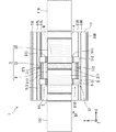
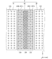
図1は、実施形態の基板処理装置の一例である塗布装置1の全体構成を模式的に示す側面図である。図2は、実施形態の塗布装置1を鉛直方向上側から見た概略平面図である。図3は、実施形態の塗布機構6を除いた塗布装置1を示す概略平面図である。図4は、図2に示すA−A線に沿う位置における塗布装置1の概略断面図である。図5は、実施形態の浮上ステージ部3の一部を示す概略平面図である。
図6は、ノズル支持体601および測定ユニット70を示す概略平面図である。図7は、ノズル61、測定ユニット70及び緩衝部80を示す概略側面図である。図8は、ノズル61、測定ユニット70及び緩衝部80を示す概略正面図である。
図7および図8に示すように、ノズル支持体601の−X側の側面における中央部には、緩衝部80が取り付けられている。緩衝部80は、Y軸方向(第2方向D2)に延びる板状の部材であり、YZ平面に平行に配置されている。緩衝部80は、吐出口611(ノズル61の下端部)と第1方向D1に重なる位置に設けられている。
塗布装置1は、塗布ステージ32による基板Wの鉛直位置の分布を取得する検査(以下、鉛直位置測定処理とも称する。)を行う。上述したように、塗布ステージ32において、吸引口322hは、雰囲気の吸引を行うため、異物を吸引する場合がある。この場合、吸引口322hに詰まりが起こることによって、浮上基板Wの浮上高さが不足するなど、浮上高さに異常が発生する可能性がある。鉛直位置測定処理は、このような浮上高さの異常を検出するために行われる。鉛直位置測定処理は、塗布装置1における基板Wの製造スケジュールに応じて、適宜のタイミングで行われるとよい。例えば、ロットの先頭基板、毎日の先頭基板、毎日午後の先頭基板を塗布処理するタイミングで行われてもよいし、すべての基板Wについて塗布処理するタイミングで行われてもよい。
以上、実施形態について説明してきたが、本発明は上記のようなものに限定されるものではなく、様々な変形が可能である。
3 浮上ステージ部(浮上機構)
31 入口浮上ステージ
32 塗布ステージ
321h 噴出口
322h 吸引口
33 出口浮上ステージ
5 搬送機構
6 塗布機構
601 ノズル支持体
61 ノズル
611 吐出口
63 ノズル移動機構
70 測定ユニット
72 測定器
72a 投光部
72b 受光部
74 連結具
76 測定器移動部
80 緩衝部
9 制御ユニット
D1 第1方向
D2 第2方向
L11 塗布位置
L13 予備吐出位置
L14 洗浄位置
ML1,ML2 位置
S11 搬入工程
S12,S12a 測定工程
S13 搬出工程
S14 塗布工程
W 基板、浮上基板
Wf 上面(第1主面)
Claims (9)
- 第1主面及び第2主面を有する基板を処理する基板処理装置であって、
前記第1主面が鉛直方向の上向きの基板に浮上力を付与する浮上機構と、
前記浮上力が付与されている前記基板である浮上基板を水平方向である第1方向に移動させる搬送機構と、
前記第1方向に直交する水平方向である第2方向に延びる吐出口を有し、前記浮上基板の前記第1主面に向けて処理液を前記吐出口から吐出可能なノズルと、
前記浮上基板の鉛直位置を測定する測定器と、
前記測定器を前記第2方向に移動させる測定器移動部と、
を備える、基板処理装置。 - 請求項1の基板処理装置であって、
前記測定器移動部は、前記測定器を前記第2方向及び前記第1方向の上流側及び下流側に移動させる、基板処理装置。 - 請求項2の基板処理装置であって、
前記ノズルに対して前記第1方向の上流側の位置であって、少なくとも前記ノズルの前記吐出口の先端部と水平方向に重なる位置に設けられる緩衝部、
をさらに備える、基板処理装置。 - 請求項3の基板処理装置であって、
前記測定器移動機構は、前記測定器を、前記ノズルからの前記処理液が前記浮上基板に付着する水平位置である付着水平位置における前記浮上基板の鉛直位置を測定可能な位置から、前記ノズルが前記処理液を吐出するときの前記緩衝部の水平位置における前記浮上基板の鉛直位置を測定可能な位置までの間で前記第2方向に移動させる、基板処理装置。 - 請求項1から請求項4のいずれか1項の基板処理装置であって、
前記第2方向の異なる位置で前記浮上基板の鉛直位置を測定する複数の前記測定器を有する、基板処理装置。 - 請求項5の基板処理装置であって、
前記複数の測定器を連結する連結具、
をさらに備え、
前記測定器移動部は、前記連結具を前記第2方向に移動させる、基板処理装置。 - 請求項1から請求項6のいずれか1項の基板処理装置であって、
前記浮上機構は、
水平面を有するステージと、
前記水平面に設けられ、前記鉛直方向の上側に向けてエアを噴出する複数の噴出口と、
前記水平面に設けられ、前記鉛直方向の上側のエアを吸引する複数の吸引口と、
を含む、基板処理装置。 - 請求項1から請求項7のいずれか1項の基板処理装置であって、
前記測定器移動機構は、前記浮上基板の前記第1方向下流側の端部が前記ステージの前記第1方向下流側の縁部に配された状態で、前記測定器を前記第2方向に移動させる、基板処理装置。 - 第1主面及び第2主面を有する基板を処理する基板処理方法であって、
(a)前記第1主面が鉛直方向の上向きの基板に浮上力を付与する工程と、
(b)前記工程(a)によって浮上力が付与されている前記基板である浮上基板を水平方向である第1方向に移動させる工程と、
(c)前記浮上基板の鉛直位置を測定する測定器を、前記第1方向に直交する水平方向である第2方向に移動させることにより、前記浮上基板における前記第2方向の複数点における鉛直位置を測定する工程と、
を含む、基板処理方法。
Priority Applications (4)
| Application Number | Priority Date | Filing Date | Title |
|---|---|---|---|
| JP2018126654A JP6722723B2 (ja) | 2018-07-03 | 2018-07-03 | 基板処理装置および基板処理方法 |
| TW108120913A TWI760621B (zh) | 2018-07-03 | 2019-06-17 | 基板處理裝置及基板處理方法 |
| KR1020190078889A KR102525265B1 (ko) | 2018-07-03 | 2019-07-01 | 기판 처리 장치 및 기판 처리 방법 |
| CN201910595463.XA CN110676192B (zh) | 2018-07-03 | 2019-07-03 | 基板处理装置和基板处理方法 |
Applications Claiming Priority (1)
| Application Number | Priority Date | Filing Date | Title |
|---|---|---|---|
| JP2018126654A JP6722723B2 (ja) | 2018-07-03 | 2018-07-03 | 基板処理装置および基板処理方法 |
Publications (2)
| Publication Number | Publication Date |
|---|---|
| JP2020006282A true JP2020006282A (ja) | 2020-01-16 |
| JP6722723B2 JP6722723B2 (ja) | 2020-07-15 |
Family
ID=69068874
Family Applications (1)
| Application Number | Title | Priority Date | Filing Date |
|---|---|---|---|
| JP2018126654A Active JP6722723B2 (ja) | 2018-07-03 | 2018-07-03 | 基板処理装置および基板処理方法 |
Country Status (4)
| Country | Link |
|---|---|
| JP (1) | JP6722723B2 (ja) |
| KR (1) | KR102525265B1 (ja) |
| CN (1) | CN110676192B (ja) |
| TW (1) | TWI760621B (ja) |
Cited By (1)
| Publication number | Priority date | Publication date | Assignee | Title |
|---|---|---|---|---|
| CN115739522A (zh) * | 2021-09-02 | 2023-03-07 | 株式会社斯库林集团 | 基板处理装置及基板处理方法 |
Families Citing this family (1)
| Publication number | Priority date | Publication date | Assignee | Title |
|---|---|---|---|---|
| KR102805961B1 (ko) * | 2022-11-01 | 2025-05-12 | 세메스 주식회사 | 약액 토출 장치 및 약액 토출 장치의 부상량 측정 방법 |
Citations (4)
| Publication number | Priority date | Publication date | Assignee | Title |
|---|---|---|---|---|
| JP2005228881A (ja) * | 2004-02-12 | 2005-08-25 | Tokyo Electron Ltd | 浮上式基板搬送処理方法及びその装置 |
| JP2006297317A (ja) * | 2005-04-22 | 2006-11-02 | Dainippon Printing Co Ltd | 塗工方法 |
| JP2012134419A (ja) * | 2010-12-24 | 2012-07-12 | Tokyo Ohka Kogyo Co Ltd | 塗布装置及び塗布方法 |
| JP2018043200A (ja) * | 2016-09-15 | 2018-03-22 | 株式会社Screenホールディングス | 塗布装置および塗布方法 |
Family Cites Families (9)
| Publication number | Priority date | Publication date | Assignee | Title |
|---|---|---|---|---|
| JP2007204278A (ja) * | 2006-02-02 | 2007-08-16 | Asahi Kosan Kk | 基板浮上搬送装置 |
| JP4942589B2 (ja) * | 2007-08-30 | 2012-05-30 | 東京応化工業株式会社 | 塗布装置及び塗布方法 |
| JP2009237485A (ja) * | 2008-03-28 | 2009-10-15 | Nec Lcd Technologies Ltd | 現像装置及び現像方法 |
| JP2010034309A (ja) * | 2008-07-29 | 2010-02-12 | Dainippon Screen Mfg Co Ltd | 塗布装置および基板処理システム |
| KR101175284B1 (ko) * | 2009-09-15 | 2012-08-21 | 주식회사 탑 엔지니어링 | 페이스트 디스펜서 및 그 제어방법 |
| JP5486030B2 (ja) | 2012-02-15 | 2014-05-07 | 東京エレクトロン株式会社 | 塗布装置 |
| JP6146029B2 (ja) * | 2013-01-31 | 2017-06-14 | 三星ダイヤモンド工業株式会社 | 形状測定装置および撮像装置 |
| CN103383468B (zh) * | 2013-06-28 | 2016-07-06 | 京东方科技集团股份有限公司 | 封框胶涂布设备的检测系统及检测方法、封框胶涂布机 |
| WO2015158390A1 (en) * | 2014-04-17 | 2015-10-22 | Applied Materials, Inc. | Carrier for substrates |
-
2018
- 2018-07-03 JP JP2018126654A patent/JP6722723B2/ja active Active
-
2019
- 2019-06-17 TW TW108120913A patent/TWI760621B/zh active
- 2019-07-01 KR KR1020190078889A patent/KR102525265B1/ko active Active
- 2019-07-03 CN CN201910595463.XA patent/CN110676192B/zh active Active
Patent Citations (4)
| Publication number | Priority date | Publication date | Assignee | Title |
|---|---|---|---|---|
| JP2005228881A (ja) * | 2004-02-12 | 2005-08-25 | Tokyo Electron Ltd | 浮上式基板搬送処理方法及びその装置 |
| JP2006297317A (ja) * | 2005-04-22 | 2006-11-02 | Dainippon Printing Co Ltd | 塗工方法 |
| JP2012134419A (ja) * | 2010-12-24 | 2012-07-12 | Tokyo Ohka Kogyo Co Ltd | 塗布装置及び塗布方法 |
| JP2018043200A (ja) * | 2016-09-15 | 2018-03-22 | 株式会社Screenホールディングス | 塗布装置および塗布方法 |
Cited By (2)
| Publication number | Priority date | Publication date | Assignee | Title |
|---|---|---|---|---|
| CN115739522A (zh) * | 2021-09-02 | 2023-03-07 | 株式会社斯库林集团 | 基板处理装置及基板处理方法 |
| CN115739522B (zh) * | 2021-09-02 | 2024-09-27 | 株式会社斯库林集团 | 基板处理装置及基板处理方法 |
Also Published As
| Publication number | Publication date |
|---|---|
| JP6722723B2 (ja) | 2020-07-15 |
| TW202012291A (zh) | 2020-04-01 |
| CN110676192A (zh) | 2020-01-10 |
| TWI760621B (zh) | 2022-04-11 |
| CN110676192B (zh) | 2024-08-27 |
| KR20200004260A (ko) | 2020-01-13 |
| KR102525265B1 (ko) | 2023-04-24 |
Similar Documents
| Publication | Publication Date | Title |
|---|---|---|
| KR101299816B1 (ko) | 도포 방법 및 도포 장치 | |
| JP5346643B2 (ja) | 基板塗布装置および基板塗布方法 | |
| CN108305843B (zh) | 基板处理装置及基板处理装置的异常状况检测方法 | |
| JP2010232472A (ja) | 基板搬送装置および基板処理装置 | |
| TWI670788B (zh) | 基板處理裝置 | |
| JP5303129B2 (ja) | 塗布装置及び塗布方法 | |
| KR20120116880A (ko) | 도포장치 | |
| JP2018043200A (ja) | 塗布装置および塗布方法 | |
| KR102525265B1 (ko) | 기판 처리 장치 및 기판 처리 방법 | |
| CN108305847B (zh) | 基板搬运装置、基板搬运方法以及基板处理装置 | |
| JP6817986B2 (ja) | ステージ測定治具、塗布装置およびステージ測定方法 | |
| JP2018143942A (ja) | 塗布装置および塗布方法 | |
| JP2011082230A (ja) | 基板塗布装置 | |
| JP6737649B2 (ja) | 塗布装置および塗布方法 | |
| JP2009022822A (ja) | 塗布装置及び塗布方法 | |
| KR102474713B1 (ko) | 기판 처리 장치 및 기판 처리 방법 | |
| JP2018147977A (ja) | 浮上量算出装置、塗布装置および塗布方法 | |
| JP2019161144A (ja) | 基板処理装置および基板処理装置の異状検知方法 |
Legal Events
| Date | Code | Title | Description |
|---|---|---|---|
| A621 | Written request for application examination |
Free format text: JAPANESE INTERMEDIATE CODE: A621 Effective date: 20190401 |
|
| A977 | Report on retrieval |
Free format text: JAPANESE INTERMEDIATE CODE: A971007 Effective date: 20200316 |
|
| A131 | Notification of reasons for refusal |
Free format text: JAPANESE INTERMEDIATE CODE: A131 Effective date: 20200324 |
|
| A521 | Request for written amendment filed |
Free format text: JAPANESE INTERMEDIATE CODE: A523 Effective date: 20200519 |
|
| TRDD | Decision of grant or rejection written | ||
| A01 | Written decision to grant a patent or to grant a registration (utility model) |
Free format text: JAPANESE INTERMEDIATE CODE: A01 Effective date: 20200602 |
|
| A61 | First payment of annual fees (during grant procedure) |
Free format text: JAPANESE INTERMEDIATE CODE: A61 Effective date: 20200622 |
|
| R150 | Certificate of patent or registration of utility model |
Ref document number: 6722723 Country of ref document: JP Free format text: JAPANESE INTERMEDIATE CODE: R150 |
|
| R250 | Receipt of annual fees |
Free format text: JAPANESE INTERMEDIATE CODE: R250 |
|
| R250 | Receipt of annual fees |
Free format text: JAPANESE INTERMEDIATE CODE: R250 |
|
| R250 | Receipt of annual fees |
Free format text: JAPANESE INTERMEDIATE CODE: R250 |