JP2020006540A - Image forming device - Google Patents
Image forming device Download PDFInfo
- Publication number
- JP2020006540A JP2020006540A JP2018127904A JP2018127904A JP2020006540A JP 2020006540 A JP2020006540 A JP 2020006540A JP 2018127904 A JP2018127904 A JP 2018127904A JP 2018127904 A JP2018127904 A JP 2018127904A JP 2020006540 A JP2020006540 A JP 2020006540A
- Authority
- JP
- Japan
- Prior art keywords
- latent image
- light
- light emitting
- line position
- image line
- Prior art date
- Legal status (The legal status is an assumption and is not a legal conclusion. Google has not performed a legal analysis and makes no representation as to the accuracy of the status listed.)
- Pending
Links
Images



Landscapes
- Facsimile Scanning Arrangements (AREA)
- Fax Reproducing Arrangements (AREA)
- Laser Beam Printer (AREA)
- Exposure Or Original Feeding In Electrophotography (AREA)
- Control Or Security For Electrophotography (AREA)
Abstract
【課題】 複数の光源素子の発光量のバラツキに起因する濃度ムラを適切に抑制する。【解決手段】 露光装置2aは、発光素子アレイで複数の光線を発光させて感光体ドラム1aに照射して静電潜像を形成する。露光装置2aは、実潜像ライン位置で光線を主走査方向に走査しつつ照射して実潜像ライン位置で静電潜像を形成するとともに、2つの実潜像ライン位置で光線を主走査方向に走査しつつ照射して2つの実潜像ライン位置の間の虚潜像ライン位置で静電潜像を形成する。そして、コントローラー31は、上述の発光素子アレイにおける複数の発光素子を順番に発光させて発光光量を測定し、その複数の発光素子について測定された発光光量に基づいて、虚潜像ライン位置での濃度ムラが抑制されるように、虚潜像ライン位置で静電潜像を形成する際の発光素子の1ドットあたりの発光時間を個別的に補正する。【選択図】 図2PROBLEM TO BE SOLVED: To appropriately suppress density unevenness due to variations in light emission amounts of a plurality of light source elements. An exposure device 2a forms a electrostatic latent image by causing a light emitting element array to emit a plurality of light rays and irradiating the light ray on a photosensitive drum 1a. The exposure device 2a irradiates the light beam while scanning the light beam in the main scanning direction at the real latent image line position to form an electrostatic latent image at the real latent image line position, and also performs the main scanning light beam at the two real latent image line positions. Irradiate while scanning in the direction to form an electrostatic latent image at a virtual latent image line position between two real latent image line positions. Then, the controller 31 sequentially causes the plurality of light emitting elements in the light emitting element array to emit light to measure the amount of emitted light, and based on the amount of emitted light measured for the plurality of light emitting elements, the virtual latent image line position The light emission time per dot of the light emitting element when the electrostatic latent image is formed at the virtual latent image line position is individually corrected so that the density unevenness is suppressed. [Selection diagram]
Description
本発明は、画像形成装置に関するものである。 The present invention relates to an image forming apparatus.
画像形成装置において、露光装置におけるポリゴンミラーの面倒れに起因して、レーザー光線の走査位置に周期的なジッターが発生し、走査位置間のピッチが変動することがある。走査位置間のピッチが変動すると、副走査方向の濃度ムラや色ズレが発生する。そこで、ある画像形成装置は、複数の光源を使用して、露光光量分布のピークをシフトさせたり、発光光源を選択することで、濃度ムラや色ズレを抑制している(例えば特許文献1,2参照)。また、別の画像形成装置では、ジッターに合わせて露光光量を変化させることで、濃度ムラを抑制している(例えば特許文献3参照)。
In an image forming apparatus, a periodic jitter may occur at a scanning position of a laser beam due to a surface tilt of a polygon mirror in an exposure apparatus, and a pitch between scanning positions may fluctuate. When the pitch between the scanning positions fluctuates, density unevenness and color shift in the sub-scanning direction occur. Therefore, some image forming apparatuses use a plurality of light sources to shift the peak of the exposure light amount distribution or select a light emitting light source to suppress density unevenness and color shift (for example,
他方、ある画像形成装置では、擬似高解像度化の手段として、インターリーブ走査方式が採用され、実潜像ライン位置で物理的にレーザー光線を走査し、2つの実潜像ライン位置の間における虚潜像ライン位置で、静電潜像を形成している。つまり、虚潜像ライン位置では物理的にレーザー光線を走査せずに、虚潜像ライン位置での静電潜像が形成される。 On the other hand, an image forming apparatus employs an interleaved scanning method as a means for increasing the pseudo-resolution, in which a laser beam is physically scanned at a real latent image line position, and a virtual latent image between two real latent image line positions is formed. An electrostatic latent image is formed at the line position. That is, an electrostatic latent image is formed at the virtual latent image line position without physically scanning the laser beam at the virtual latent image line position.
上述のようにしてジッターに合わせて露光光量を変化させることで、実潜像ライン位置での濃度ムラは抑制できるが、インターリーブ走査方式の虚潜像ライン位置での濃度には複数の実潜像ライン位置での露光光量が関与しているため、虚潜像ライン位置での濃度ムラは、上述の方法では適切に抑制されない可能性がある。また、上述のように複数の光源を使用して濃度ムラを抑制する場合、光源のコスト、ひいては画像形成装置のコストが高くなってしまう。 By changing the exposure light amount in accordance with the jitter as described above, the density unevenness at the actual latent image line position can be suppressed. Since the amount of exposure light at the line position is involved, the density unevenness at the virtual latent image line position may not be appropriately suppressed by the above method. Further, when the density unevenness is suppressed by using a plurality of light sources as described above, the cost of the light source, and eventually the cost of the image forming apparatus, increase.
しかしながら、上述のレーザー光線の光源として複数の光源素子のアレイを備えたマルチビーム光源を使用する場合、複数の光源素子の発光量のバラツキがあっても、実潜像ライン位置は変動しないが、インターリーブ走査方式の虚潜像ライン位置での濃度には複数の実潜像ライン位置での露光光量が関与しているため、複数の光源素子の発光量のバラツキに起因して虚潜像ライン位置が変動してしまい、虚潜像ライン位置の変動に起因する濃度ムラが発生する可能性がある。 However, when a multi-beam light source having an array of a plurality of light source elements is used as the light source of the above-mentioned laser beam, the actual latent image line position does not fluctuate even if the light emission amount of the plurality of light source elements fluctuates, but the interleaving is performed. Since the exposure amount at a plurality of real latent image line positions is related to the density at the virtual latent image line position in the scanning method, the virtual latent image line position may be reduced due to the variation in the light emission amount of a plurality of light source elements. It may fluctuate, and density unevenness may occur due to the fluctuation of the virtual latent image line position.
本発明は、上記の問題に鑑みてなされたものであり、複数の光源素子の発光量のバラツキに起因する濃度ムラを適切に抑制する画像形成装置を得ることを目的とする。 The present invention has been made in view of the above problems, and has as its object to provide an image forming apparatus that appropriately suppresses density unevenness caused by variations in the amount of light emitted from a plurality of light source elements.
本発明に係る画像形成装置は、感光体ドラムと、発光素子アレイで複数の光線を発光させて前記感光体ドラムに照射して静電潜像を形成する露光装置と、前記静電潜像にトナーを付着させてトナー像を生成する現像装置と、前記露光装置を制御するコントローラーとを備える。前記露光装置は、実潜像ライン位置で前記光線を主走査方向に走査しつつ照射して実潜像ライン位置で前記静電潜像を形成するとともに、2つの実潜像ライン位置で前記光線を主走査方向に走査しつつ照射して前記2つの実潜像ライン位置の間の虚潜像ライン位置で前記静電潜像を形成する。前記コントローラーは、前記発光素子アレイにおける複数の発光素子を順番に発光させて発光光量を測定し、前記複数の発光素子について測定された前記発光光量に基づいて、前記虚潜像ライン位置での濃度ムラが抑制されるように、前記虚潜像ライン位置で前記静電潜像を形成する際の前記発光素子の1ドットあたりの発光時間を個別的に補正する。 An image forming apparatus according to the present invention includes a photosensitive drum, an exposure device that emits a plurality of light beams by a light emitting element array and irradiates the photosensitive drum to form an electrostatic latent image. The image forming apparatus includes a developing device that generates a toner image by attaching toner, and a controller that controls the exposure device. The exposure device irradiates the light beam while scanning it in the main scanning direction at the actual latent image line position to form the electrostatic latent image at the actual latent image line position, and at the two actual latent image line positions, Is irradiated while scanning in the main scanning direction to form the electrostatic latent image at a virtual latent image line position between the two real latent image line positions. The controller measures the amount of emitted light by sequentially emitting light from the plurality of light emitting elements in the light emitting element array, and, based on the amount of emitted light measured for the plurality of light emitting elements, the density at the position of the virtual latent image line. The light emission time per dot of the light emitting element when forming the electrostatic latent image at the virtual latent image line position is individually corrected so that unevenness is suppressed.
本発明によれば、複数の光源素子の発光量のバラツキに起因する濃度ムラを適切に抑制する画像形成装置が得られる。 According to the present invention, it is possible to obtain an image forming apparatus that appropriately suppresses density unevenness caused by variations in the light emission amounts of a plurality of light source elements.
本発明の上記又は他の目的、特徴および優位性は、添付の図面とともに以下の詳細な説明から更に明らかになる。 The above and other objects, features and advantages of the present invention will become more apparent from the following detailed description in conjunction with the accompanying drawings.
以下、図に基づいて本発明の実施の形態を説明する。 Hereinafter, an embodiment of the present invention will be described with reference to the drawings.
図1は、本発明の実施の形態に係る画像形成装置の機械的な内部構成の一部を示す側面図である。図1に示す画像形成装置は、プリンター、ファクシミリ装置、複写機、複合機などといった、電子写真方式の印刷機能を有する装置である。 FIG. 1 is a side view showing a part of a mechanical internal configuration of an image forming apparatus according to an embodiment of the present invention. The image forming apparatus illustrated in FIG. 1 is an apparatus having an electrophotographic printing function, such as a printer, a facsimile machine, a copier, and a multifunction peripheral.
この実施の形態の画像形成装置は、タンデム方式のカラー現像装置を有する。このカラー現像装置は、感光体ドラム1a〜1d、露光装置2a〜2dおよび現像装置3a〜3dを有する。感光体ドラム1a〜1dは、シアン、マゼンタ、イエローおよびブラックの4色の感光体である。
The image forming apparatus of this embodiment has a tandem type color developing device. This color developing device has
露光装置2a〜2dは、レーザー光線を感光体ドラム1a〜1dに照射して静電潜像を形成する。露光装置2a〜2dは、レーザー光線の光源であるレーザーダイオード、そのレーザー光線を感光体ドラム1a〜1dへ導く光学素子(レンズ、ミラー、ポリゴンミラーなど)を有する。
The
各露光装置2a〜2dは、発光素子アレイで複数の光線を発光させて感光体ドラムに照射して静電潜像を形成する。
Each of the
さらに、感光体ドラム1a〜1dの周囲には、スコロトロン等の帯電器、クリーニング装置、除電器などが配置されている。クリーニング装置は、1次転写後に、感光体ドラム1a〜1d上の残留トナーを除去し、除電器は、1次転写後に、感光体ドラム1a〜1dを除電する。
Further, a charger such as a scorotron, a cleaning device, a static eliminator, and the like are arranged around the
現像装置3a〜3dには、シアン、マゼンタ、イエローおよびブラックの4色のトナーが充填されているトナーカートリッジがそれぞれ装着され、トナーカートリッジからトナーが供給され、キャリアとともに現像剤を構成する。現像装置3a〜3dは、そのトナーを感光体ドラム1a〜1d上の静電潜像に付着させてトナー像を形成する。
To the developing
このように、各現像装置3a〜3dは、感光体ドラム1a〜1d上の静電潜像にトナーを付着させてトナー像を生成する。
As described above, each of the developing
感光体ドラム1a、露光装置2a、および現像装置3aにより、マゼンタの現像が行われ、感光体ドラム1b、露光装置2b、および現像装置3bにより、シアンの現像が行われ、感光体ドラム1c、露光装置2c、および現像装置3cにより、イエローの現像が行われ、感光体ドラム1d、露光装置2d、および現像装置3dにより、ブラックの現像が行われる。
Magenta development is performed by the
中間転写ベルト4は、感光体ドラム1a〜1dに接触し、感光体ドラム1a〜1d上のトナー画像を1次転写される環状の像担持体である。中間転写ベルト4は、駆動ローラー5に張架され、駆動ローラー5からの駆動力によって、感光体ドラム1dとの接触位置から感光体ドラム1aとの接触位置への方向へ周回していく。
The
転写ローラー6は、搬送されてくる用紙を中間転写ベルト4に接触させ、中間転写ベルト4上のトナー画像を用紙に2次転写する。なお、トナー画像を転写された用紙は、定着器9へ搬送され、トナー画像が用紙へ定着される。
The transfer roller 6 brings the conveyed sheet into contact with the
ローラー7は、クリーニングブラシを有し、クリーニングブラシを中間転写ベルト4に接触させ、用紙へのトナー画像の転写後に中間転写ベルト4に残ったトナーを除去する。
The roller 7 has a cleaning brush, contacts the cleaning brush with the
センサー8は、現像されたトナー像の濃度を測定する光学式センサーであって、中間転写ベルト4に光線を照射し、その反射光を検出する。例えば、各種調整の際、センサー8は、中間転写ベルト4の所定箇所に光線を照射しその反射光を検出し、その所定箇所を通過するパッチ画像(均一濃度の所定形状のトナー画像)に応じた電気信号を出力する。
The
レジストローラー10は、給紙トレイなどから1次給紙で搬送されてくる用紙を一時停止させ、2次給紙タイミングでその用紙を中間転写ベルト4および転写ローラー6による転写位置へ搬送する。2次給紙タイミングは、その用紙上の指定された位置に中間転写ベルト4上のトナー画像が転写されるように指定される。レジストセンサー11は、レジストローラー10の近傍に設置され、用紙がレジストローラー10(レジストレーション位置)へ到達したことを光学的に検出するセンサーである。
The
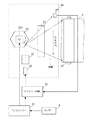
図2は、図1における露光装置2aの構成およびその周辺の電子回路の構成の一例を示す図である。なお、図2に示す露光装置は、感光体ドラム1a用の露光装置2aであり、感光体ドラム1b〜1d用の露光装置2b〜2dも同様の構成を有する。
FIG. 2 is a diagram showing an example of the configuration of the
図2において、光源21は、レーザー光線を出射する光源である。光学系22は、光源21からポリゴンミラー23までの間、および/またはポリゴンミラー23から感光体ドラム1aおよびPDセンサー24までの間に配置された各種レンズ群である。光学系22には、fθレンズなどが使用される。
In FIG. 2, a
光源21は、複数のレーザー光線を出射する発光素子アレイを備える。この実施の形態では、この発光素子アレイは、モノリシックレーザーダイオードアレイである。
The
また、ポリゴンミラー23は、感光体ドラム1aの軸に対して垂直な軸を有し、その軸に垂直な断面が多角形であり、その側面がミラーとなっている素子である。ポリゴンミラー23は、その軸を中心に回転し、光源21から出射したレーザー光線を感光体ドラム1aの軸方向(主走査方向)に沿って走査する。ポリゴンモーターユニット23aは、コントローラー31からの制御信号に従ってポリゴンミラー23を回転させる。
The
また、PDセンサー24は、主走査同期信号を生成するためにポリゴンミラー23により走査されているレーザー光線を所定位置で受光するセンサーである。PDセンサー24は、光が入射すると、光量に応じた出力電圧を誘起する。PDセンサー24は、光が走査される線上の所定の位置に配置され、光のスポットがその位置を通過するタイミングを検出し、そのタイミングで形成されるパルスを主走査同期信号として出力する。
The PD sensor 24 is a sensor that receives a laser beam scanned by the
コントローラー31は、ASIC(Application Specific Integrated Circuit)やコンピューターなどを備え、当該画像形成装置の内部装置の制御やデータ処理などを行い、露光装置2a(光源21、ドライバー回路32など)を制御し、画像形成のためにレーザー光線で感光体ドラム1aを露光する。
The
ドライバー回路32は、光源21を制御してレーザー光線を出射させる回路である。ドライバー回路32は、主走査同期信号に同期して形成すべき画像に応じたパターンでレーザー光線によって露光されるように光源21を制御する。ドライバー回路32は、コントローラー31からの制御信号に従って、光源21の複数の発光素子に対してそれぞれ個別的に発光制御(発光のオンオフ)を行う。
The
図3は、擬似高解像度化技術を説明する図である。図3に示すように、露光装置2aは、擬似高解像度化技術を使用して静電潜像を形成する。具体的には、この露光装置2aは、実潜像ライン位置でレーザー光線を照射して実潜像ライン位置で静電潜像を形成するとともに、2つの実潜像ライン位置でレーザー光線を照射してその2つの実潜像ライン位置の間の虚潜像ライン位置で静電潜像を形成する。なお、実潜像ライン位置のレーザー光線の光量(強度または照射時間)を調整することで、実潜像ライン位置でトナー像が現像されずに、虚潜像ライン位置でトナー像が現像されるようにすることができる。
FIG. 3 is a diagram illustrating a pseudo high resolution technique. As shown in FIG. 3, the
さらに、コントローラー31は、光源21の発光素子アレイにおける複数の発光素子を順番に発光させて発光光量を測定し、その複数の発光素子について測定された発光光量に基づいて、虚潜像ライン位置での濃度ムラが抑制されるように発光素子の1ドットあたりの発光時間を個別的に補正する。
Further, the
図4は、図2における光源21が2つの発光素子を備えるアレイである場合の2つの発光素子の発光光量差のない場合の実潜像ライン位置および虚潜像ライン位置のピッチを説明する図である。図5は、図2における光源21が2つの発光素子を備える場合の2つの発光素子の発光光量差のある場合の実潜像ライン位置および虚潜像ライン位置のピッチを説明する図である。
FIG. 4 is a diagram for explaining pitches of a real latent image line position and a virtual latent image line position when there is no difference between the light emission amounts of the two light emitting elements when the
発光光量差がない場合、図4に示すように、実潜像ライン位置および虚潜像ライン位置のピッチは均一になっているが、例えば図5に示すように、発光光量差がある場合(例えば図5に示すように、第1発光素子の発光光量が第2発光素子の発光光量より低い場合)、実潜像ライン位置と隣接する実潜像ライン位置とのピッチの一方が狭くなり他方が広くなる。 When there is no difference in the amount of emitted light, as shown in FIG. 4, the pitch between the actual latent image line position and the position of the imaginary latent image line are uniform, but, for example, as shown in FIG. For example, as shown in FIG. 5, when the amount of light emitted from the first light emitting element is lower than the amount of light emitted from the second light emitting element), one of the pitches between the actual latent image line position and the adjacent actual latent image line position becomes narrower, and the other. Becomes wider.
コントローラー31は、発光光量の低い発光素子の1ドットあたりの発光時間を、発光光量の高い発光素子の発光時間より長くして、両者の発光光量を互いに近づける。
The
なお、1ドット(1画素)あたり発光時間(時間長)は、例えば8ビットの信号でコントローラー31によりドライバー回路32により指定され、256段階で調整可能となっている。
The light emission time (time length) per dot (one pixel) is specified by the
具体的には、コントローラー31は、(a)上述の複数の発光素子から1つずつ発光素子を選択し、(b)選択した発光素子の発光時間(つまり、発光光量)を変化させて静電潜像を形成させ、形成された静電潜像に対応するトナー像の濃度をセンサー8に測定させ、測定した濃度から発光光量を特定し、(c)その複数の発光素子に対応して測定された発光光量および対応する発光時間に基づいて、虚潜像ライン位置での濃度ムラが抑制されるように、虚潜像ライン位置で静電潜像を形成する際の発光素子の1ドットあたりの発光時間を個別的に補正する。
Specifically, the
例えば、コントローラー31は、測定された濃度が所定濃度となる発光時間を各発光素子について特定し、特定した発光時間の比率を特定し、その比率に基づいて、(a)発光光量の低い発光素子の発光時間を長くすることにより、(b)発光光量の高い発光素子の発光時間を短くすることにより、あるいは(c)その両方を行うことにより、その複数の発光素子の発光光量を、互いに一致するように可能な限り近づける。
For example, the
また、コントローラー31は、(a)虚潜像ライン位置で静電潜像を形成せずに実潜像ライン位置で静電潜像を形成して、実潜像ライン位置によるトナー像の濃度をセンサー8に測定させ、(b)実潜像ライン位置で静電潜像を形成せずに虚潜像ライン位置で静電潜像を形成して、虚潜像ライン位置によるトナー像の濃度をセンサー8に測定させ、(c)ある1つの濃度指定値(画像データにおけるある1つの画素値)に対して、実潜像ライン位置によるトナー像の濃度と虚潜像ライン位置によるトナー像の濃度とが一致するように、(c1)虚潜像ライン位置で静電潜像を形成する際の発光素子の1ドットあたりの発光時間または(c2)実潜像ライン位置で静電潜像を形成する際の発光素子の1ドットあたりの発光時間を個別的に補正する。
The
次に、上記画像形成装置の動作について説明する。図6は、図1および図2に示す画像形成装置の動作について説明するフローチャートである。 Next, the operation of the image forming apparatus will be described. FIG. 6 is a flowchart illustrating the operation of the image forming apparatus illustrated in FIGS. 1 and 2.
調整の際に、まず、コントローラー31は、上述のように、(a)実潜像ライン位置によるトナー像(パッチ画像)の濃度をセンサー8に測定させ、(b)虚潜像ライン位置によるトナー像(パッチ画像)の濃度をセンサー8に測定させ、(c)実潜像ライン位置によるトナー像の濃度と虚潜像ライン位置によるトナー像の濃度とが一致するように、(c1)虚潜像ライン位置で静電潜像を形成する際の発光素子の1ドットあたりの発光時間または(c2)実潜像ライン位置で静電潜像を形成する際の発光素子の1ドットあたりの発光時間を個別的に補正する(ステップS1)。
At the time of the adjustment, first, as described above, the
次に、コントローラー31は、光源21の複数の発光素子から1つの発光素子を選択し(ステップS2)、選択した発光素子のみを使用して、選択した発光素子の発光時間を変化させつつ、パッチ画像に対応して発光素子を発光させる(ステップS3)。コントローラー31は、各発光時間でのパッチ画像のトナー濃度をセンサー8で測定し、トナー濃度が所定濃度となる発光時間を特定する(ステップS4)。
Next, the
そして、コントローラー31は、光源21のすべての発光素子の発光特性(つまり、トナー濃度が所定濃度となる発光時間)を特定したか否かを判定し(ステップS5)、発光特性を特定していない発光素子があれば、ステップS2に戻り、発光特性を特定していない発光素子を1つ選択し(ステップS2)、同様の処理を実行する。
Then, the
このようにして、コントローラー31は、すべての発光素子の発光特性を特定すると、上述のようにして、発光素子の発光時間を個別的に補正する(ステップS6)。
After specifying the light emission characteristics of all the light emitting elements in this way, the
以上のように、上記実施の形態によれば、露光装置2a〜2dは、発光素子アレイで複数の光線を発光させて感光体ドラム1a〜1dに照射して静電潜像を形成する。さらに、露光装置2a〜2dは、実潜像ライン位置で光線を主走査方向に走査しつつ照射して実潜像ライン位置で静電潜像を形成するとともに、2つの実潜像ライン位置で光線を主走査方向に走査しつつ照射して2つの実潜像ライン位置の間の虚潜像ライン位置で静電潜像を形成する。そして、コントローラー31は、上述の発光素子アレイにおける複数の発光素子を順番に発光させて発光光量を測定し、その複数の発光素子について測定された発光光量に基づいて、虚潜像ライン位置での濃度ムラが抑制されるように、虚潜像ライン位置で静電潜像を形成する際の発光素子の1ドットあたりの発光時間を個別的に補正する。
As described above, according to the above embodiment, the
これにより、光源21における複数の光源素子の発光量のバラツキに起因する濃度ムラが適切に抑制される。
Thereby, the density unevenness due to the variation in the light emission amount of the plurality of light source elements in the
なお、上述の実施の形態に対する様々な変更および修正については、当業者には明らかである。そのような変更および修正は、その主題の趣旨および範囲から離れることなく、かつ、意図された利点を弱めることなく行われてもよい。つまり、そのような変更および修正が請求の範囲に含まれることを意図している。 Various changes and modifications to the above-described embodiment will be apparent to those skilled in the art. Such changes and modifications may be made without departing from the spirit and scope of the subject matter and without diminishing its intended advantages. That is, such changes and modifications are intended to be included in the scope of the claims.
例えば、上記実施の形態では、トナー濃度をセンサー8で測定することで上述の発光光量を測定しているが、ビームスプリッターなどの光学素子で発光光線の一部を所定割合で分岐させ、分岐した発光光線の一部をフォトダイオードなどの受光素子で受光してその受光光量を測定することで、上述の発光光量を測定するようにしてもよい。
For example, in the above-described embodiment, the above-described light emission amount is measured by measuring the toner concentration with the
また、上記実施の形態において、ステップS6での調整後にステップS1と同様の処理を行って、実潜像ライン位置によるトナー像の濃度と虚潜像ライン位置によるトナー像の濃度とが一致するように、実潜像ライン位置で静電潜像を形成する際の発光素子の1ドットあたりの発光時間を個別的に補正するようにしてもよい。 In the above embodiment, after the adjustment in step S6, the same processing as in step S1 is performed so that the toner image density based on the actual latent image line position matches the toner image density based on the imaginary latent image line position. Alternatively, the light emission time per dot of the light emitting element when forming an electrostatic latent image at the actual latent image line position may be individually corrected.
本発明は、例えば、電子写真方式の画像形成装置に適用可能である。 The present invention is applicable to, for example, an electrophotographic image forming apparatus.
1a〜1d 感光体ドラム
2a〜2d 露光装置
3a〜3d 現像装置
31 コントローラー
1a-
Claims (4)
発光素子アレイで複数の光線を発光させて前記感光体ドラムに照射して静電潜像を形成する露光装置と、
前記静電潜像にトナーを付着させてトナー像を生成する現像装置と、
前記露光装置を制御するコントローラーとを備え、
前記露光装置は、実潜像ライン位置で前記光線を主走査方向に走査しつつ照射して実潜像ライン位置で前記静電潜像を形成するとともに、2つの実潜像ライン位置で前記光線を主走査方向に走査しつつ照射して前記2つの実潜像ライン位置の間の虚潜像ライン位置で前記静電潜像を形成し、
前記コントローラーは、前記発光素子アレイにおける複数の発光素子を順番に発光させて発光光量を測定し、前記複数の発光素子について測定された前記発光光量に基づいて、前記虚潜像ライン位置での濃度ムラが抑制されるように、虚潜像ライン位置で前記静電潜像を形成する際の前記発光素子の1ドットあたりの発光時間を個別的に補正すること、
を特徴とする画像形成装置。 A photosensitive drum,
An exposure apparatus that forms a latent electrostatic image by irradiating the photosensitive drum with a plurality of light rays emitted by a light emitting element array,
A developing device that generates a toner image by attaching toner to the electrostatic latent image;
A controller for controlling the exposure apparatus,
The exposure device irradiates the light beam while scanning it in the main scanning direction at the actual latent image line position to form the electrostatic latent image at the actual latent image line position, and the light beam at the two actual latent image line positions. Irradiating while scanning in the main scanning direction to form the electrostatic latent image at a virtual latent image line position between the two real latent image line positions,
The controller measures the amount of emitted light by sequentially emitting light from the plurality of light emitting elements in the light emitting element array, and, based on the amount of emitted light measured for the plurality of light emitting elements, the density at the position of the virtual latent image line. Individually correcting the light emission time per dot of the light emitting element when forming the electrostatic latent image at the virtual latent image line position so that unevenness is suppressed;
An image forming apparatus comprising:
前記コントローラーは、(a)前記複数の発光素子から1つずつ発光素子を選択し、(b)選択した前記発光素子の前記発光時間を変化させて前記静電潜像を形成させ、形成された前記静電潜像に対応する前記トナー像の濃度を前記センサーに測定させ、測定した前記濃度から前記発光光量を特定し、(c)前記複数の発光素子に対応して測定された前記発光光量および前記発光時間に基づいて、前記虚潜像ライン位置での濃度ムラが抑制されるように、前記虚潜像ライン位置で前記静電潜像を形成する際の前記発光素子の1ドットあたりの発光時間を個別的に補正すること、
を特徴とする請求項1記載の画像形成装置。 Further comprising a sensor for measuring the density of the toner image,
The controller is configured to (a) select one light emitting element from the plurality of light emitting elements one by one, and (b) change the light emission time of the selected light emitting element to form the electrostatic latent image. Causing the sensor to measure the density of the toner image corresponding to the electrostatic latent image; identifying the amount of emitted light from the measured density; and (c) determining the amount of emitted light corresponding to the plurality of light emitting elements. And based on the light emission time, so that the density unevenness at the virtual latent image line position is suppressed, so that the light emitting element per dot of the light emitting element when forming the electrostatic latent image at the virtual latent image line position Correcting the emission time individually,
The image forming apparatus according to claim 1, wherein:
Priority Applications (1)
| Application Number | Priority Date | Filing Date | Title |
|---|---|---|---|
| JP2018127904A JP2020006540A (en) | 2018-07-04 | 2018-07-04 | Image forming device |
Applications Claiming Priority (1)
| Application Number | Priority Date | Filing Date | Title |
|---|---|---|---|
| JP2018127904A JP2020006540A (en) | 2018-07-04 | 2018-07-04 | Image forming device |
Publications (1)
| Publication Number | Publication Date |
|---|---|
| JP2020006540A true JP2020006540A (en) | 2020-01-16 |
Family
ID=69150180
Family Applications (1)
| Application Number | Title | Priority Date | Filing Date |
|---|---|---|---|
| JP2018127904A Pending JP2020006540A (en) | 2018-07-04 | 2018-07-04 | Image forming device |
Country Status (1)
| Country | Link |
|---|---|
| JP (1) | JP2020006540A (en) |
Cited By (1)
| Publication number | Priority date | Publication date | Assignee | Title |
|---|---|---|---|---|
| US20220091533A1 (en) * | 2020-09-24 | 2022-03-24 | Fujifilm Business Innovation Corp. | Light emitting device and image forming apparatus |
-
2018
- 2018-07-04 JP JP2018127904A patent/JP2020006540A/en active Pending
Cited By (2)
| Publication number | Priority date | Publication date | Assignee | Title |
|---|---|---|---|---|
| US20220091533A1 (en) * | 2020-09-24 | 2022-03-24 | Fujifilm Business Innovation Corp. | Light emitting device and image forming apparatus |
| US11762309B2 (en) * | 2020-09-24 | 2023-09-19 | Fujifilm Business Innovation Corp. | Light emitting device and image forming apparatus |
Similar Documents
| Publication | Publication Date | Title |
|---|---|---|
| JP2016173489A (en) | Image forming apparatus and image forming method | |
| US8582997B2 (en) | Image forming apparatus | |
| US8836748B2 (en) | Optical unit, light scanning device, and image forming apparatus | |
| JP6031228B2 (en) | Light beam detection circuit, light beam scanning unit, and image forming apparatus | |
| US8421835B2 (en) | Exposure device capable of stabilizing density of image formed by multiple exposure and image forming apparatus equipped with the exposure device | |
| JP5679919B2 (en) | Exposure apparatus and image forming apparatus | |
| JP5713932B2 (en) | Image forming apparatus | |
| JP2013163308A (en) | Image forming apparatus and image forming method | |
| JP6864852B2 (en) | Image forming device | |
| JP5543404B2 (en) | Image forming apparatus | |
| JP2013076728A (en) | Image forming apparatus | |
| US11099498B2 (en) | Image forming apparatus | |
| JP6091404B2 (en) | Image forming apparatus | |
| JP5918119B2 (en) | Image forming apparatus | |
| JP2020118854A (en) | Image forming apparatus | |
| JP6091408B2 (en) | Image forming apparatus | |
| JP5713820B2 (en) | Exposure apparatus and image forming apparatus | |
| JP2019191383A (en) | Image forming apparatus | |
| JP2024164860A (en) | Image forming device | |
| JP2007322745A (en) | Image forming apparatus | |
| JP2023025609A (en) | Image forming apparatus | |
| JP2015058561A (en) | Image forming apparatus and image forming method | |
| JP6165112B2 (en) | Image forming apparatus | |
| JP2001113749A (en) | Image forming apparatus | |
| JP4998378B2 (en) | Laser scanning optical device |