JP2020008444A - Wiring open detection circuit - Google Patents
Wiring open detection circuit Download PDFInfo
- Publication number
- JP2020008444A JP2020008444A JP2018130394A JP2018130394A JP2020008444A JP 2020008444 A JP2020008444 A JP 2020008444A JP 2018130394 A JP2018130394 A JP 2018130394A JP 2018130394 A JP2018130394 A JP 2018130394A JP 2020008444 A JP2020008444 A JP 2020008444A
- Authority
- JP
- Japan
- Prior art keywords
- wiring
- open
- terminal
- test bus
- diode
- Prior art date
- Legal status (The legal status is an assumption and is not a legal conclusion. Google has not performed a legal analysis and makes no representation as to the accuracy of the status listed.)
- Granted
Links
Images


Classifications
-
- G—PHYSICS
- G01—MEASURING; TESTING
- G01R—MEASURING ELECTRIC VARIABLES; MEASURING MAGNETIC VARIABLES
- G01R31/00—Arrangements for testing electric properties; Arrangements for locating electric faults; Arrangements for electrical testing characterised by what is being tested not provided for elsewhere
- G01R31/50—Testing of electric apparatus, lines, cables or components for short-circuits, continuity, leakage current or incorrect line connections
- G01R31/66—Testing of connections, e.g. of plugs or non-disconnectable joints
- G01R31/67—Testing the correctness of wire connections in electric apparatus or circuits
-
- G—PHYSICS
- G01—MEASURING; TESTING
- G01R—MEASURING ELECTRIC VARIABLES; MEASURING MAGNETIC VARIABLES
- G01R31/00—Arrangements for testing electric properties; Arrangements for locating electric faults; Arrangements for electrical testing characterised by what is being tested not provided for elsewhere
- G01R31/28—Testing of electronic circuits, e.g. by signal tracer
- G01R31/2851—Testing of integrated circuits [IC]
- G01R31/2884—Testing of integrated circuits [IC] using dedicated test connectors, test elements or test circuits on the IC under test
-
- G—PHYSICS
- G01—MEASURING; TESTING
- G01R—MEASURING ELECTRIC VARIABLES; MEASURING MAGNETIC VARIABLES
- G01R31/00—Arrangements for testing electric properties; Arrangements for locating electric faults; Arrangements for electrical testing characterised by what is being tested not provided for elsewhere
- G01R31/50—Testing of electric apparatus, lines, cables or components for short-circuits, continuity, leakage current or incorrect line connections
- G01R31/54—Testing for continuity
Landscapes
- Engineering & Computer Science (AREA)
- Physics & Mathematics (AREA)
- General Physics & Mathematics (AREA)
- Computer Hardware Design (AREA)
- Microelectronics & Electronic Packaging (AREA)
- General Engineering & Computer Science (AREA)
- Tests Of Electronic Circuits (AREA)
- Semiconductor Integrated Circuits (AREA)
- Testing Of Short-Circuits, Discontinuities, Leakage, Or Incorrect Line Connections (AREA)
Abstract
【課題】複数の配線のオープン検出を簡略な構成を用いて実行する。
【解決手段】一つの実施形態によれば、配線オープン検出回路は、信号処理回路、端子、ダイオード、テストバス、オープン判定回路を含む。信号処理回路は、第1配線の一端に接続され、信号処理した信号を第1配線に出力する。端子は、第1配線の他端に接続される。ダイオードは、一端が端子に接続される。テストバスは、一端がダイオードの他端に接続される。オープン判定回路は、テストバスの他端に接続され、テストバスを介してダイオードの他端に第1電圧を印加し、第1配線に流れる電流の変化を検出して第1配線がオープンか否かを判定する。
【選択図】図1An open detection of a plurality of wirings is performed using a simple configuration.
According to one embodiment, a wiring open detection circuit includes a signal processing circuit, a terminal, a diode, a test bus, and an open determination circuit. The signal processing circuit is connected to one end of the first wiring, and outputs a signal subjected to signal processing to the first wiring. The terminal is connected to the other end of the first wiring. One end of the diode is connected to the terminal. One end of the test bus is connected to the other end of the diode. The open determination circuit is connected to the other end of the test bus, applies a first voltage to the other end of the diode via the test bus, detects a change in current flowing through the first wiring, and determines whether the first wiring is open. Is determined.
[Selection diagram] Fig. 1
Description
本発明の実施形態は、配線オープン検出回路に関する。 Embodiments of the present invention relate to a wiring open detection circuit.
近年、半導体集積回路では、多数の機能を取り込んでシステム化及び高集積化、半導体集積回路を多数用いてマルチチップパッケージ化やマルチチップモジュール化等が進行している。半導体集積回路の配線数の多数本化や配線の長距離化、半導体集積回路チップ間を接続する配線の長距離化も進展している。 2. Description of the Related Art In recent years, in semiconductor integrated circuits, systemization and high integration by incorporating a large number of functions, multi-chip packaging and multi-chip modules using a large number of semiconductor integrated circuits have been advanced. Increasing the number of wires in semiconductor integrated circuits, increasing the length of wires, and increasing the length of wires connecting between semiconductor integrated circuit chips are also progressing.
このため、半導体集積回路では、配線のオープンやショートを検出するのは大変重要となっている。これらの配線のオープンやショート検出する方法として、例えば光信号や電気信号等を用いた不良解析装置が多用されている。不良解析装置を用いた場合、解析の事前準備、解析対応ソフト等が必要となり、簡略な構成で迅速な不良解析が困難であるという問題点がある。 For this reason, in a semiconductor integrated circuit, it is very important to detect an open or short circuit of a wiring. As a method of detecting the open or short of these wirings, for example, a failure analyzer using an optical signal, an electric signal, or the like is often used. When a failure analysis device is used, advance preparation for analysis, analysis support software, and the like are required, and there is a problem that it is difficult to quickly perform failure analysis with a simple configuration.
本発明は、複数の配線のオープン検出を簡略な構成を用いて実行することができる配線オープン検出回路を提供することにある。 An object of the present invention is to provide a wiring open detection circuit that can execute open detection of a plurality of wirings using a simple configuration.
一つの実施形態によれば、配線オープン検出回路は、信号処理回路、端子、ダイオード、テストバス、オープン判定回路を含む。信号処理回路は、 第1配線の一端に接続され、信号処理した信号を第1配線に出力する。端子は、第1配線の他端に接続される。ダイオードは、一端が端子に接続される。テストバスは、一端がダイオードの他端に接続される。オープン判定回路は、テストバスの他端に接続され、テストバスを介してダイオードの他端に第1電圧を印加し、第1配線に流れる電流の変化を検出して第1配線がオープンか否かを判定する。 According to one embodiment, the wiring open detection circuit includes a signal processing circuit, a terminal, a diode, a test bus, and an open determination circuit. The signal processing circuit is connected to one end of the first wiring, and outputs a signal processed signal to the first wiring. The terminal is connected to the other end of the first wiring. One end of the diode is connected to the terminal. One end of the test bus is connected to the other end of the diode. The open determination circuit is connected to the other end of the test bus, applies a first voltage to the other end of the diode via the test bus, detects a change in current flowing through the first wiring, and determines whether the first wiring is open. Is determined.
以下本発明の実施形態について図面を参照しながら説明する。 Hereinafter, embodiments of the present invention will be described with reference to the drawings.
(第1の実施形態)
まず、第1の実施形態に係る配線オープン検出回路について、図面を参照して説明する。図1は配線オープン検出回路を示す回路図である。
(1st Embodiment)
First, a wiring open detection circuit according to a first embodiment will be described with reference to the drawings. FIG. 1 is a circuit diagram showing a wiring open detection circuit.
第1の実施形態では、ドライバと端子間を接続する長距離の配線のオープン検出として、端子とオープン判定回路の間にダイオード及びテストバスを設けている。テストバスを介してダイオードに電圧を印加して長距離の配線に流れる電流の変化をオープン判定回路が検出して、長距離の配線がオープンか否かを判定している。 In the first embodiment, a diode and a test bus are provided between a terminal and an open determination circuit as open detection of a long-distance wiring connecting the driver and the terminal. A voltage is applied to the diode via the test bus, and a change in the current flowing through the long-distance wiring is detected by the open determination circuit to determine whether the long-distance wiring is open.
図1に示すように、配線オープン検出回路100は、ドライバDRIV1〜DRIV4、ドライバDRIVn−1、ドライバDRIVn、配線MW1〜MW4、配線MWn−1、配線MWn、端子PAD1〜PAD4、端子PADn−1、端子PADn、ダイオードD1〜D4、ダイオードDn−1、ダイオードDn、テストバスTB、オープン判定回路1を含む。
As shown in FIG. 1, the wiring
第1の実施形態では、ドライバDRIV1〜DRIV4、ドライバDRIVn−1、ドライバDRIVn、配線MW1〜MW4、配線MWn−1、配線MWn、端子PAD1〜PAD4、端子PADn−1、及び端子PADnを含む半導体集積回路(図示せず)に、ダイオードD1〜D4、ダイオードDn−1、ダイオードDn、テストバスTBを設けて長距離の配線である配線MW1〜MW4、配線MWn−1、配線MWnがオープンか否かを判定している。 In the first embodiment, a semiconductor integrated circuit including drivers DRIV1 to DRIV4, driver DRIVn-1, driver DRIVn, wirings MW1 to MW4, wiring MWn-1, wiring MWn, terminals PAD1 to PAD4, terminal PADn-1, and terminal PADn. A circuit (not shown) is provided with diodes D1 to D4, a diode Dn-1, a diode Dn, and a test bus TB to determine whether wirings MW1 to MW4, wirings MWn-1, and wiring MWn, which are long distance wirings, are open. Is determined.
ドライバDRIV1〜DRIV4、ドライバDRIVn−1、ドライバDRIVnは、半導体集積回路の出力側に設けられる信号処理を実行する信号処理回路である。 The drivers DRIV1 to DRIV4, the driver DRIVn-1, and the driver DRIVn are signal processing circuits provided on the output side of the semiconductor integrated circuit and performing signal processing.
配線MW1〜MW4、配線MWn−1、配線MWnは、配線長が1mm以上(例えば、7mm)の金属配線であり、並列配置されている。 The wirings MW1 to MW4, the wiring MWn-1, and the wiring MWn are metal wirings having a wiring length of 1 mm or more (for example, 7 mm), and are arranged in parallel.
配線MW1は、一端がドライバDRIV1に接続され、他端が端子PAD1に接続され、ドライバDRIV1で実行される信号処理信号を端子PAD1に出力する。配線MW2は、一端がドライバDRIV2に接続され、他端が端子PAD2に接続され、ドライバDRIV2で実行される信号処理信号を端子PAD2に出力する。配線MW3は、一端がドライバDRIV3に接続され、他端が端子PAD3に接続され、ドライバDRIV3で実行される信号処理信号を端子PAD3に出力する。配線MW4は、一端がドライバDRIV4に接続され、他端が端子PAD4に接続され、ドライバDRIV4で実行される信号処理信号を端子PAD4に出力する。配線MWn−1は、一端がドライバDRIVn−1に接続され、他端が端子PADn−1に接続され、ドライバDRIVn−1で実行される信号処理信号を端子PADn−1に出力する。配線MWnは、一端がドライバDRIVnに接続され、他端が端子PADnに接続され、ドライバDRIVnで実行される信号処理信号を端子PADnに出力する。 The wiring MW1 has one end connected to the driver DRIV1, the other end connected to the terminal PAD1, and outputs a signal processing signal executed by the driver DRIV1 to the terminal PAD1. The wiring MW2 has one end connected to the driver DRIV2 and the other end connected to the terminal PAD2, and outputs a signal processing signal executed by the driver DRIV2 to the terminal PAD2. The wiring MW3 has one end connected to the driver DRIV3, the other end connected to the terminal PAD3, and outputs a signal processing signal executed by the driver DRIV3 to the terminal PAD3. The wiring MW4 has one end connected to the driver DRIV4 and the other end connected to the terminal PAD4, and outputs a signal processing signal executed by the driver DRIV4 to the terminal PAD4. The wiring MWn-1 has one end connected to the driver DRIVn-1 and the other end connected to the terminal PADn-1, and outputs a signal processing signal executed by the driver DRIVn-1 to the terminal PADn-1. The wiring MWn has one end connected to the driver DRIVn and the other end connected to the terminal PADn, and outputs a signal processing signal executed by the driver DRIVn to the terminal PADn.
ダイオードD1は、一端(カソード)が端子PAD1に接続され、他端(アノード)がテストバスTBに接続される。ダイオードD2は、一端(カソード)が端子PAD2に接続され、他端(アノード)がテストバスTBに接続される。ダイオードD3は、一端(カソード)が端子PAD3に接続され、他端(アノード)がテストバスTBに接続される。ダイオードD4は、一端(カソード)が端子PAD4に接続され、他端(アノード)がテストバスTBに接続される。ダイオードDn−1は、一端(カソード)が端子PADn−1に接続され、他端(アノード)がテストバスTBに接続される。ダイオードDnは、一端(カソード)が端子PADnに接続され、他端(アノード)がテストバスTBに接続される。オープン判定回路1は、テストバスTBに接続される。
One end (cathode) of the diode D1 is connected to the terminal PAD1, and the other end (anode) is connected to the test bus TB. One end (cathode) of the diode D2 is connected to the terminal PAD2, and the other end (anode) is connected to the test bus TB. One end (cathode) of the diode D3 is connected to the terminal PAD3, and the other end (anode) is connected to the test bus TB. One end (cathode) of the diode D4 is connected to the terminal PAD4, and the other end (anode) is connected to the test bus TB. One end (cathode) of the diode Dn-1 is connected to the terminal PADn-1, and the other end (anode) is connected to the test bus TB. One end (cathode) of the diode Dn is connected to the terminal PADn, and the other end (anode) is connected to the test bus TB.
隣接配置される長距離の配線間のショート不良は、例えば隣接配置されるドライバからの電流を検出して配線間がショートしているか否かを判定する。ここでは、詳細の説明は省略する。 The short-circuit failure between adjacently disposed long-distance wirings is determined by detecting a current from a driver disposed adjacently, for example, to determine whether or not the wirings are short-circuited. Here, the detailed description is omitted.
次に、配線オープン試験について図2、図3A及び図3Bを参照して説明する。図2は、配線オープン試験を示す回路図である。図3Aは、配線オープン試験での印加電圧を示す図である。図3Bは、配線オープン試験での判定結果を示す図である。ここでは、配線MW1のオープン試験を例にして説明する。配線MW2〜MW4、配線MWn−1、配線MWnのオープン試験については、配線MW1と同様なので説明を省略する。 Next, the wiring open test will be described with reference to FIGS. 2, 3A and 3B. FIG. 2 is a circuit diagram showing a wiring open test. FIG. 3A is a diagram showing applied voltages in a wiring open test. FIG. 3B is a diagram illustrating a determination result in the wiring open test. Here, an open test of the wiring MW1 will be described as an example. The open test of the wirings MW2 to MW4, the wiring MWn-1, and the wiring MWn is the same as that of the wiring MW1, and the description is omitted.
図2に示すように、ドライバDRIV1は、トランジスタPMT1とトランジスタNMT1から構成される出力バッファである。トランジスタPMT1は、Pch MOSトランジスタであり、ソースが電源(高電位側電源)VDD1に接続され、ドレインが配線MW1の一端に接続される。トランジスタNMT1は、Nch MOSトランジスタであり、ドレインがトランジスタPMT1のドレインと配線MW1の一端に接続され、ソースが接地電位(低電位側電源)Vssに接続される。 As shown in FIG. 2, the driver DRIV1 is an output buffer including a transistor PMT1 and a transistor NMT1. The transistor PMT1 is a Pch MOS transistor. The source is connected to the power supply (high-potential-side power supply) VDD1, and the drain is connected to one end of the wiring MW1. The transistor NMT1 is an Nch MOS transistor. The drain is connected to the drain of the transistor PMT1 and one end of the wiring MW1, and the source is connected to the ground potential (low-potential-side power supply) Vss.
オープン判定回路1は、一端がテストバスTBに接続され、他端がMOSトランジスタNMT1のソースに接続されている。
The
配線オープン試験のときに、オープン判定回路1は、テストバスTBを介してダイオードD1の他端(アノード)にテストバス印加電圧Vtb(第1電圧)を印加する。オープン判定回路1は、配線MW1(第1配線)に流れる電流Itestの変化を検出して配線MW1がオープンか否かを判定する。
At the time of the wiring open test, the
図3Aに示すように、半導体集積回路の通常動作時では、オープン判定回路1が印加するテストバス印加電圧Vtbは接地電位Vssに設定され、例えばドライバDRIV1から出力される信号は端子PAD1を介して外部に出力される。
As shown in FIG. 3A, during the normal operation of the semiconductor integrated circuit, the test bus applied voltage Vtb applied by the
配線オープン試験のときに、オープン判定回路1が印加するテストバス印加電圧VtbはダイオードD1の順方向電圧よりも大きな正の電圧(第1電圧)に設定される。
At the time of the wiring open test, the test bus applied voltage Vtb applied by the
図3Bに示すように、オープン判定回路1は、配線MW1に流れる電流Itestが変化する場合は配線MW1が配線正常(断線していない)と判定し、配線MW1に流れる電流Itestが一定(変化なし)の場合は配線MW1がオープン不良であると判定する。
As shown in FIG. 3B, when the current Itest flowing through the wiring MW1 changes, the
上述したように、本実施形態の配線オープン検出回路100では、ドライバDRIV1〜DRIV4、ドライバDRIVn−1、ドライバDRIVn、配線MW1〜MW4、配線MWn−1、配線MWn、端子PAD1〜PAD4、端子PADn−1、端子PADn、ダイオードD1〜D4、ダイオードDn−1、ダイオードDn、テストバスTB、オープン判定回路1が設けられる。オープン判定回路1は、テストバスTBを介してダイオードD1の他端にテストバス印加電圧Vtbを印加する。オープン判定回路1は、配線MW1に流れる電流Itestの変化を検出して配線MW1がオープンか否かを判定する。
As described above, in the wiring
このため、複数の配線のオープンか否かの判定を迅速に、簡略な構成を用いて実行することができる。 Therefore, it is possible to quickly determine whether or not a plurality of wirings are open using a simple configuration.
なお、第1の実施形態では、ダイオードのカソードを端子に接続し、ダイオードのアノードをテストデバイスに接続しているが必ずしもこれに限定されるものではない。例えば、図10に示す第1の変形例の配線オープン検出回路100aにしてもよい。
In the first embodiment, the cathode of the diode is connected to the terminal, and the anode of the diode is connected to the test device. However, the present invention is not limited to this. For example, the wiring
具体的には、図10に示すように、ダイオードD31は、アノードが端子PAD1に接続カソードがテストバスTBに接続されている。ダイオードD32は、アノードが端子PAD2に接続カソードがテストバスTBに接続されている。ダイオードD33は、アノードが端子PAD3に接続カソードがテストバスTBに接続されている。ダイオードD34は、アノードが端子PAD4に接続カソードがテストバスTBに接続されている。ダイオードD3n−1は、アノードが端子PADn−1に接続カソードがテストバスTBに接続されている。ダイオードD3nは、アノードが端子PADnに接続カソードがテストバスTBに接続されている。テストバスTBはオープン判定回路21に接続されている。
Specifically, as shown in FIG. 10, the diode D31 has an anode connected to the terminal PAD1 and a cathode connected to the test bus TB. The diode D32 has an anode connected to the terminal PAD2 and a cathode connected to the test bus TB. The diode D33 has an anode connected to the terminal PAD3 and a cathode connected to the test bus TB. The diode D34 has an anode connected to the terminal PAD4 and a cathode connected to the test bus TB. The diode D3n-1 has an anode connected to the terminal PADn-1 and a cathode connected to the test bus TB. The diode D3n has an anode connected to the terminal PADn and a cathode connected to the test bus TB. The test bus TB is connected to the
図11Aに示すように、配線オープン試験のときに、オープン判定回路21は、テストバスTBを介してダイオードD31の他端(カソード)にテストバス印加電圧Vtb(第1電圧)を印加する。オープン判定回路21は、配線MW1(第1配線)に流れる電流Itestの変化を検出して配線MW1がオープンか否かを判定する。
As shown in FIG. 11A, at the time of the wiring open test, the
図11Bに示すように、配線オープン試験のときに、オープン判定回路21が印加するテストバス印加電圧VtbはダイオードD1の耐圧よりも大きな正の電圧(第1電圧)に設定される。オープン判定回路21は、配線MW1に流れる電流Itestが変化する場合は配線MW1が配線正常(断線していない)と判定し、配線MW1に流れる電流Itestが一定(変化なし)の場合は配線MW1がオープン不良であると判定する。
As shown in FIG. 11B, at the time of the wiring open test, the test bus applied voltage Vtb applied by the
(第2の実施形態)
次に、第2の実施形態に係る配線オープン検出回路に係るについて、図面を参照して説明する。図4は配線オープン検出回路を示す回路図である。
(Second embodiment)
Next, a wiring open detection circuit according to a second embodiment will be described with reference to the drawings. FIG. 4 is a circuit diagram showing a wiring open detection circuit.
第2の実施形態では、ドライバと端子間を接続する長距離の配線のオープン検出として、端子とオープン判定回路の間にキャパシタを設けている。キャパシタに充電された電荷が放電されたときに、オープン判定回路に設けられたアナログ・デジタルコンバータが放電電圧の変化を検出して長距離の配線がオープンか否かを判定している。 In the second embodiment, a capacitor is provided between a terminal and an open determination circuit as open detection of a long-distance wiring connecting the driver and the terminal. When the charge stored in the capacitor is discharged, an analog-to-digital converter provided in the open determination circuit detects a change in the discharge voltage and determines whether the long-distance wiring is open.
以下、第1の実施形態と同一構成部分には、同一符号を付してその部分の説明を省略し、異なる部分のみ説明する。 Hereinafter, the same components as those of the first embodiment are denoted by the same reference numerals, and the description of those components will be omitted. Only different components will be described.
図4に示すように、配線オープン検出回路101は、ドライバDRIV1〜DRIV4、ドライバDRIVn−1、ドライバDRIVn、配線MW1〜MW4、配線MWn−1、配線MWn、端子PAD1〜PAD4、端子PADn−1、端子PADn、キャパシタC1〜C4、キャパシタCn−1、キャパシタCn、スイッチSW1、スイッチSW2、テストバスTB1、テストバスTB2、オープン判定回路1aを含む。
As shown in FIG. 4, the wiring
第1の実施形態では、ドライバDRIV1〜DRIV4、ドライバDRIVn−1、ドライバDRIVn、配線MW1〜MW4、配線MWn−1、配線MWn、端子PAD1〜PAD4、端子PADn−1、及び端子PADnを含む半導体集積回路(図示せず)に、キャパシタC1〜C4、キャパシタCn−1、キャパシタCn、スイッチSW1、スイッチSW2、テストバスTB1、テストバスTB2を設けて長距離の配線である配線MW1〜MW4、配線MWn−1、配線MWnがオープンか否かを判定している。 In the first embodiment, a semiconductor integrated circuit including drivers DRIV1 to DRIV4, driver DRIVn-1, driver DRIVn, wirings MW1 to MW4, wiring MWn-1, wiring MWn, terminals PAD1 to PAD4, terminal PADn-1, and terminal PADn. A circuit (not shown) is provided with capacitors C1 to C4, a capacitor Cn-1, a capacitor Cn, a switch SW1, a switch SW2, a test bus TB1, and a test bus TB2, and wirings MW1 to MW4, which are long distance wirings, and a wiring MWn. -1, It is determined whether or not the wiring MWn is open.
キャパシタC1は、端子PAD1とテストバスTB1の間に設けられる配線間容量であり、ドライバDRIV1から出力される出力信号により電荷を充電する。キャパシタC3は、端子PAD3とテストバスTB1の間に設けられる配線間容量であり、ドライバDRIV3から出力される出力信号により電荷を充電する。キャパシタCn−1は、端子PADn−1とテストバスTB1の間に設けられる配線間容量であり、ドライバDRIVn−1から出力される出力信号により電荷を充電する。 The capacitor C1 is an inter-wire capacitance provided between the terminal PAD1 and the test bus TB1, and charges an electric charge with an output signal output from the driver DRIV1. The capacitor C3 is an inter-wiring capacitance provided between the terminal PAD3 and the test bus TB1, and charges an electric charge by an output signal output from the driver DRIV3. The capacitor Cn-1 is an inter-wire capacitance provided between the terminal PADn-1 and the test bus TB1, and charges the electric charge with an output signal output from the driver DRIVn-1.
キャパシタC2は、端子PAD2とテストバスTB2の間に設けられる配線間容量であり、ドライバDRIV2から出力される出力信号により電荷を充電する。キャパシタC4は、端子PAD4とテストバスTB2の間に設けられる配線間容量であり、ドライバDRIV4から出力される出力信号により電荷を充電する。キャパシタCnは、端子PADnとテストバスTB2の間に設けられる配線間容量であり、ドライバDRIVnから出力される出力信号により電荷を充電する。 The capacitor C2 is an inter-wiring capacitance provided between the terminal PAD2 and the test bus TB2, and charges an electric charge by an output signal output from the driver DRIV2. The capacitor C4 is an inter-wiring capacitance provided between the terminal PAD4 and the test bus TB2, and charges an electric charge with an output signal output from the driver DRIV4. The capacitor Cn is a capacitance between wirings provided between the terminal PADn and the test bus TB2, and charges an electric charge by an output signal output from the driver DRIVn.
スイッチSW1は、テストバスTB1とオープン判定回路1aの間に設けられる。スイッチSW2は、テストバスTB2とオープン判定回路1aの間に設けられる。
The switch SW1 is provided between the test bus TB1 and the
出力信号が一定なローレベル(Vssレベル)の信号では、キャパシタC1〜C4、キャパシタCn−1、キャパシタCnは電荷を充電しない。キャパシタC1〜C4、キャパシタCn−1、キャパシタCnは、配線間容量であるので蓄積された電荷は徐々に放電する。 When the output signal is a constant low level (Vss level) signal, the capacitors C1 to C4, the capacitor Cn-1, and the capacitor Cn do not charge. Since the capacitors C1 to C4, the capacitor Cn-1, and the capacitor Cn are capacitances between wirings, accumulated charges are gradually discharged.
ここでは、キャパシタC1〜C4、キャパシタCn−1、キャパシタCnには、配線間容量を用いているがゲート容量を用いてもよい。 Here, the capacitance between wirings is used for the capacitors C1 to C4, the capacitor Cn-1, and the capacitor Cn, but a gate capacitance may be used.
次に、配線オープン試験について図5及び図6を参照して説明する。図5は、配線オープン試験を示す回路図である。図6は、配線オープン試験での判定結果を示す図である。ここでは、配線MW1のオープン試験を例にして説明する。配線MW2〜MW4、配線MWn−1、配線MWnのオープン試験については、配線MW1と同様なので説明を省略する。 Next, the wiring open test will be described with reference to FIGS. FIG. 5 is a circuit diagram showing a wiring open test. FIG. 6 is a diagram illustrating a determination result in the wiring open test. Here, an open test of the wiring MW1 will be described as an example. The open test of the wirings MW2 to MW4, the wiring MWn-1, and the wiring MWn is the same as that of the wiring MW1, and the description is omitted.
図5に示すように、オープン判定回路1aは、一端がテストバスTB1に接続され、他端がMOSトランジスタNMT1のソースに接続され、アナログ・デジタルコンバータ2を含む。キャパシタC1は、ドライバDRIV1から出力されるハイレベルの出力信号により電荷を充電し、ドライバDRIV1の出力信号がVssレベルのときに蓄積された電荷を放電する。このとき、スイッチSW1がオンしてキャパシタC1の放電電荷がアナログ・デジタルコンバータ2の入力側に入力信号Sinとして入力される。アナログ・デジタルコンバータ2は、アナログ・デジタル変換処理を実行してデジタル信号である出力信号Soutを出力する。
As shown in FIG. 5, the
配線MW1の配線オープン試験のとき、ドライバDRIV2〜DRIV4、ドライバDRIVn−1、ドライバDRIVnから出力される出力信号は一定なVssレベルに設定するのが好ましい。その理由は、キャパシタC2〜C4、キャパシタCn−1、キャパシタCnを充放電させないためである。 At the time of the wiring open test of the wiring MW1, it is preferable that the output signals output from the drivers DRIV2 to DRIV4, the driver DRIVn-1, and the driver DRIVn are set to a constant Vss level. The reason is that the capacitors C2 to C4, the capacitor Cn-1, and the capacitor Cn are not charged and discharged.
図6に示すように、オープン判定回路1aは、アナログ・デジタルコンバータ2から出力される出力信号Soutが変化する場合(ハイレベルがVdd1/ローレベルがVss)、配線MW1が配線正常(断線していない)と判定し、アナログ・デジタルコンバータ2から出力される出力信号Soutが一定な場合(Vss)、配線MW1がオープン不良であると判定する。
As shown in FIG. 6, when the output signal Sout output from the analog-to-digital converter 2 changes (high level is Vdd1 / low level is Vss), the
上述したように、本実施形態の配線オープン検出回路101では、ドライバDRIV1〜DRIV4、ドライバDRIVn−1、ドライバDRIVn、配線MW1〜MW4、配線MWn−1、配線MWn、端子PAD1〜PAD4、端子PADn−1、端子PADn、キャパシタC1〜C4、キャパシタCn−1、キャパシタCn、スイッチSW1、スイッチSW2、テストバスTB1、テストバスTB2、オープン判定回路1aが設けられる。オープン判定回路1aは、アナログ・デジタルコンバータ2を含む。キャパシタに充電された電荷が放電されたときに、アナログ・デジタルコンバータ2が放電電圧の変化を検出し、オープン判定回路1aが長距離の配線のオープンか否かを判定している。
As described above, in the wiring
このため、複数の配線がオープンか否かの判定を迅速に、簡略な構成を用いて実行することができる。 Therefore, it is possible to quickly determine whether or not a plurality of wirings are open using a simple configuration.
なお、第2の実施形態では、端子とテストバスの間にキャパシタを設けているが必ずしもこれに限定されるものではない。例えば、図12に示すキャパシタを抵抗に置き換えた第2の変形例の配線オープン検出回路101aにしてもよい。
In the second embodiment, a capacitor is provided between the terminal and the test bus. However, the present invention is not limited to this. For example, a wiring
具体的には、図12に示すように、抵抗R1は端子PAD1とテストバスTB1の間に設けられる。抵抗R2は端子PAD2とテストバスTB2の間に設けられる。抵抗R3は端子PAD3とテストバスTB1の間に設けられる。抵抗R4は端子PAD4とテストバスTB2の間に設けられる。抵抗Rn−1は端子PADn−1とテストバスTB1の間に設けられる。抵抗Rnは端子PADnとテストバスTB2の間に設けられる。 Specifically, as shown in FIG. 12, the resistor R1 is provided between the terminal PAD1 and the test bus TB1. The resistor R2 is provided between the terminal PAD2 and the test bus TB2. The resistor R3 is provided between the terminal PAD3 and the test bus TB1. The resistor R4 is provided between the terminal PAD4 and the test bus TB2. The resistor Rn-1 is provided between the terminal PADn-1 and the test bus TB1. The resistance Rn is provided between the terminal PADn and the test bus TB2.
抵抗R1〜R4、抵抗Rn−1、抵抗Rnは、高抵抗値(例えば、数MΩ)を有する抵抗である。オープン判定回路31がスイッチSW1とスイッチSW2に接続される。
The resistors R1 to R4, the resistor Rn-1, and the resistor Rn are resistors having a high resistance value (for example, several MΩ). An
オープン判定回路31は、ドライバから出力される出力信号を高抵抗値の抵抗を介して入力し、長距離の配線に流れる電流の変化を検知して長距離の配線がオープンであるか否かを判定する。ここで、配線MW1の配線オープン試験のとき、ドライバDRIV2〜DRIV4、ドライバDRIVn−1、ドライバDRIVnから出力される出力信号は一定なVssレベルに設定するのが好ましい。
The
(第3の実施形態)
次に、第3の実施形態に係る配線オープン検出回路に係るについて、図面を参照して説明する。図7は配線オープン検出回路を示す回路図である。
(Third embodiment)
Next, a wiring open detection circuit according to a third embodiment will be described with reference to the drawings. FIG. 7 is a circuit diagram showing a wiring open detection circuit.
第3の実施形態では、第1集積回路チップに第1テストバスを設け、第2集積回路チップに第2テストバスを設けて、オープン判定回路が第1集積回路チップと第2集積回路チップを接続する配線のオープンか否かを判定している。 In the third embodiment, a first test bus is provided in a first integrated circuit chip, a second test bus is provided in a second integrated circuit chip, and the open determination circuit connects the first integrated circuit chip and the second integrated circuit chip. It is determined whether the wiring to be connected is open.
図7に示すように、配線オープン検出回路102は、集積回路チップChipA、集積回路チップChipB、配線MW11、オープン判定回路1bを含む。
As shown in FIG. 7, the wiring
集積回路チップChipAは、バッファBUFF1、端子PAD11,端子PAD12、テストバスTB11、ダイオードD11、ダイオードD12を含む。集積回路チップChipAは、多数の回路(図示しない)を内蔵する半導体集積回路である。 The integrated circuit chip ChipA includes a buffer BUFF1, a terminal PAD11, a terminal PAD12, a test bus TB11, a diode D11, and a diode D12. The integrated circuit chip ChipA is a semiconductor integrated circuit incorporating a large number of circuits (not shown).
バッファBUFF1は、MOSトランジスタPMT11とMOSトランジスタNMT11を含む入力バッファである。 The buffer BUFF1 is an input buffer including a MOS transistor PMT11 and a MOS transistor NMT11.
MOSトランジスタPMT11は、Pch MOSトランジスタであり、ソースが電源(高電位側電源)VDD1に接続され、ゲートに端子D12を介して入力される入力信号を入力する。MOSトランジスタNMT11は、Nch MOSトランジスタであり、ドレインがMOSトランジスタPMT11のドレインに接続され、ソースが接地電位(低電位側電源)Vssに接続され、ゲートに端子D12を介して入力される入力信号を入力する。 The MOS transistor PMT11 is a Pch MOS transistor, the source of which is connected to the power supply (high-potential-side power supply) VDD1, and the input signal of which is input to the gate via the terminal D12. The MOS transistor NMT11 is an Nch MOS transistor. The drain is connected to the drain of the MOS transistor PMT11, the source is connected to the ground potential (low-potential-side power supply) Vss, and the gate receives an input signal input via the terminal D12. input.
ダイオードD11は、端子PAD12とバッファBUFF1の間に設けられる低電位側の保護ダイオードである。ダイオードD11は、カソードが端子PAD2に接続される。ダイオードD12は、端子PAD12とバッファBUFF1の間に設けられる高電位側の保護ダイオードである。ダイオードD12は、カソードが電源(高電位側電源)VDD1に接続され、アノードが端子PAD12に接続される。 The diode D11 is a low-potential-side protection diode provided between the terminal PAD12 and the buffer BUFF1. The diode D11 has a cathode connected to the terminal PAD2. The diode D12 is a high-potential-side protection diode provided between the terminal PAD12 and the buffer BUFF1. The diode D12 has a cathode connected to the power supply (high-potential-side power supply) VDD1, and an anode connected to the terminal PAD12.
テストバスTB11(第1テストバス)は、一端が端子PAD11に接続され、他端がダイオードD11のアノードに接続される。 The test bus TB11 (first test bus) has one end connected to the terminal PAD11 and the other end connected to the anode of the diode D11.
集積回路チップChipBは、バッファBUFF2、端子PAD13、端子14、テストバスTB12を含む。集積回路チップChipBは、多数の回路(図示しない)を内蔵する半導体集積回路である。 The integrated circuit chip ChipB includes a buffer BUFF2, a terminal PAD13, a terminal 14, and a test bus TB12. The integrated circuit chip ChipB is a semiconductor integrated circuit incorporating a large number of circuits (not shown).
バッファBUFF2(信号処理回路)は、MOSトランジスタPMT12とMOSトランジスタNMT12を含み、出力信号を端子PAD13に出力する出力バッファである。 The buffer BUFF2 (signal processing circuit) is an output buffer that includes a MOS transistor PMT12 and a MOS transistor NMT12, and outputs an output signal to a terminal PAD13.
MOSトランジスタPMT12は、Pch MOSトランジスタであり、ソースが電源(高電位側電源)VDD1に接続され、ドレインが端子PAD13に接続される。MOSトランジスタNMT12は、Nch MOSトランジスタであり、ドレインがMOSトランジスタPMT12のドレインと端子PAD13に接続され、ソースが接地電位(低電位側電源)Vssに接続される。テストバスTB12(第2のテストバス)は、一端がMOSトランジスタNMT12のソースに接続され、他端が端子PAD14に接続される。 The MOS transistor PMT12 is a Pch MOS transistor. The source is connected to the power supply (high-potential-side power supply) VDD1, and the drain is connected to the terminal PAD13. The MOS transistor NMT12 is an Nch MOS transistor. The drain is connected to the drain of the MOS transistor PMT12 and the terminal PAD13, and the source is connected to the ground potential (low-potential-side power supply) Vss. The test bus TB12 (second test bus) has one end connected to the source of the MOS transistor NMT12 and the other end connected to the terminal PAD14.
配線MW11は、一端が端子PAD12に接続され、他端が端子PAD13に接続される。ここでは、配線MW11は積層形成される集積回路チップChipAと集積回路チップChipBを接続するビアであるが、隣接配置される集積回路チップChipAと集積回路チップChipBを接続する配線であってもよい。 One end of the wiring MW11 is connected to the terminal PAD12, and the other end is connected to the terminal PAD13. Here, the wiring MW11 is a via connecting the integrated circuit chip ChipA and the integrated circuit chip ChipB which are stacked, but may be a wiring connecting the integrated circuit chip ChipA and the integrated circuit chip ChipB which are arranged adjacently.
オープン判定回路1bは、一端が端子PAD11に接続され、他端が端子PAD14に接続される。オープン判定回路1bは、配線MW11のオープン試験のとき、テストバスTB11(第1テストバス)を介してダイオードD11のアノードにダイオードD11の順方向電圧よりも大きな正の電圧(第1電圧)であるテストバス印加電圧Vtbを印加して、配線がオープンであるか否かを判定する。
The
上述したように、本実施形態の配線オープン検出回路102では、集積回路チップChipA、集積回路チップChipB、配線MW11、オープン判定回路1bが設けられる。 集積回路チップChipAは、バッファBUFF1、端子PAD11,端子PAD12、テストバスTB11、ダイオードD11、ダイオードD12を含む。集積回路チップChipBは、バッファBUFF2、端子PAD13、端子14、テストバスTB12を含む。配線MW11は、一端が端子PAD12に接続され、他端が端子PAD13に接続される。オープン判定回路1bは、テストバスTB11を介してダイオードD11のアノードにダイオードD11の順方向電圧よりも大きな正の電圧(第1電圧)であるテストバス印加電圧Vtbを印加して、配線がオープンであるか否かを判定する。
As described above, the wiring
このため、集積回路チップChipAと集積回路チップChipBを接続する配線MW11がオープンか否かの判定を迅速に、簡略な構成を用いて実行することができる。 For this reason, it is possible to quickly determine whether the wiring MW11 connecting the integrated circuit chip ChipA and the integrated circuit chip ChipB is open or not with a simple configuration.
なお、第3の実施形態では、低電位側の保護ダイオードであるダイオードD11のアノードに電圧を印加しているが必ずしもこれに限定されるものではない。例えば、高電位側の保護ダイオードであるダイオードD12のカソードにダイオードD12の耐圧よりも大きな正の電圧(第1電圧)であるテストバス印加電圧Vtbを印加して、配線がオープンであるか否かを判定してもよい。 In the third embodiment, a voltage is applied to the anode of the diode D11, which is a protection diode on the low potential side. However, the present invention is not limited to this. For example, a test bus application voltage Vtb, which is a positive voltage (first voltage) higher than the withstand voltage of the diode D12, is applied to the cathode of the diode D12, which is a protection diode on the high potential side, and whether the wiring is open or not is determined. May be determined.
(第4の実施形態)
次に、第4の実施形態に係る配線オープン検出回路に係るについて、図面を参照して説明する。図8は配線オープン検出回路を示す回路図である。
(Fourth embodiment)
Next, a wiring open detection circuit according to a fourth embodiment will be described with reference to the drawings. FIG. 8 is a circuit diagram showing a wiring open detection circuit.
第4の実施形態では、多数の長距離の配線を有するドライバアレイチップとビアを介してドライバアレイチップに接続されるMEMSアレイチップにダイオードとテストバスを設けて、オープン判定回路がテストバス及びビアを介してドライバアレイチップの長距離の配線のオープンか否かを判定している。 In the fourth embodiment, a diode and a test bus are provided in a MEMS array chip connected to a driver array chip via a driver array chip having a large number of long-distance wirings and vias, and an open determination circuit is provided with a test bus and a via. It is determined whether or not the long-distance wiring of the driver array chip is open via.
以下、第1の実施形態と同一構成部分には、同一符号を付してその部分の説明を省略し、異なる部分のみ説明する。 Hereinafter, the same components as those of the first embodiment are denoted by the same reference numerals, and the description of those components will be omitted. Only different components will be described.
図8に示すように、配線オープン検出回路103は、ドライバDRIV1、配線MW21、オープン判定回路11a、オープン判定回路11b、テストバスTB21、テストバスTB22、ダイオードD21、ダイオードD22、電極DNK1〜DNK3、ビアVIA1、ビアVIA2を含む。
As shown in FIG. 8, the wiring
ドライバDRIV1、配線MW21、テストバスTB21、テストバスTB22、ダイオードD21、ダイオードD22、電極DNK1、電極DNK2は、多数の長距離の配線を有するドライバアレイチップ(図示しない)に含まれる。電極DNK3は、MEMSアレイチップ(図示しない)に含まれる。MEMSアレイチップは、ビアVIA1、ビアVIA2を介してドライバアレイチップに接続され、ドライバアレイチップ上に積層形成される。 The driver DRIV1, the wiring MW21, the test bus TB21, the test bus TB22, the diode D21, the diode D22, the electrode DNK1, and the electrode DNK2 are included in a driver array chip (not shown) having many long-distance wirings. The electrode DNK3 is included in a MEMS array chip (not shown). The MEMS array chip is connected to the driver array chip via the vias VIA1 and VIA2, and is formed on the driver array chip.
配線MW21は、一端がドライバDRIV1に接続され、他端が電極DNK1に接続される長距離の配線である。電極DNK2は、電極DNK1に隣接配置され、例えばドライバアレイチップの同じ層に設けられる電極である。電極DNK3は、MEMSアレイチップの電極であり、一端がビアVIA1を介して電極DNK1に接続され、他端がビアVIA2を介して電極DNK2に接続される。 The wiring MW21 is a long-distance wiring having one end connected to the driver DRIV1 and the other end connected to the electrode DNK1. The electrode DNK2 is an electrode arranged adjacent to the electrode DNK1 and provided on the same layer of the driver array chip, for example. The electrode DNK3 is an electrode of the MEMS array chip. One end is connected to the electrode DNK1 via the via VIA1, and the other end is connected to the electrode DNK2 via the via VIA2.
ダイオードD21は、カソードが電極DNK1に接続され、アノードがテストバスTB21に接続される。ダイオードD22は、カソードが電極DNK2に接続され、アノードがテストバスTB22に接続される。 The diode D21 has a cathode connected to the electrode DNK1 and an anode connected to the test bus TB21. The diode D22 has a cathode connected to the electrode DNK2 and an anode connected to the test bus TB22.
オープン判定回路11aは、一端がテストバスTB21に接続され、他端がMOSトランジスタNMT1のソースに接続されている。オープン判定回路11bは、一端がテストバスTB22に接続され、他端がMOSトランジスタNMT1のソースに接続されている。
The
オープン判定回路11aは、配線オープン試験のときにダイオードD21のアノードにテストバス印加電圧Vtb1を印加する。オープン判定回路11bは、配線オープン試験のときにダイオードD22のアノードにテストバス印加電圧Vtb2を印加する。
The
次に、配線オープン試験について図9A、図9Bを参照して説明する。図9Aは配線オープン試験での印加電圧を示す図である。図9Bは、配線オープン試験での判定結果を示す図である。 Next, the wiring open test will be described with reference to FIGS. 9A and 9B. FIG. 9A is a diagram showing applied voltages in a wiring open test. FIG. 9B is a diagram illustrating a determination result in the wiring open test.
図9Aに示すように、ドライバアレイチップ及びMEMSアレイチップが通常動作のとき、テストバス印加電圧Vtb1とテストバス印加電圧Vtb2は、接地電位Vssに設定される。 As shown in FIG. 9A, when the driver array chip and the MEMS array chip operate normally, the test bus applied voltage Vtb1 and the test bus applied voltage Vtb2 are set to the ground potential Vss.
配線オープンテストIのとき、ダイオードD21の順方向電圧よりも大きな正のテストバス印加電圧Vtb1がダイオードD21のアノードに印加され、接地電位Vssのテストバス印加電圧Vtb2がダイオードD22のアノードに印加される。配線オープンテストIのとき、オープン判定回路11aは、テストバスTB21〜ダイオードD21〜電極DNK1〜配線MW21の経路の配線に流れる電流の変化を検知し、配線がオープンであるか否かを判定する。
At the time of the wiring open test I, a positive test bus applied voltage Vtb1 larger than the forward voltage of the diode D21 is applied to the anode of the diode D21, and the test bus applied voltage Vtb2 of the ground potential Vss is applied to the anode of the diode D22. . At the time of the wiring open test I, the
配線オープンテストIIのとき、ダイオードD22の順方向電圧よりも大きな正のテストバス印加電圧Vtb2がダイオードD22のアノードに印加され、接地電位Vssのテストバス印加電圧Vtb1がダイオードD21のアノードに印加される。配線オープンテストIIのとき、オープン判定回路11bは、テストバスTB22〜ダイオードD22〜電極DNK2〜ビアVIA2〜電極DNK3〜ビアVIA1〜電極DNK1〜配線MW21の経路の配線に流れる電流の変化を検知し、配線がオープンであるか否かを判定する。配線オープンテストIIでは、MEMSアレイチップを介してドライバアレイチップの長距離の配線MW21がオープンであるか否かが判定される。
In the wiring open test II, a positive test bus applied voltage Vtb2 larger than the forward voltage of the diode D22 is applied to the anode of the diode D22, and the test bus applied voltage Vtb1 of the ground potential Vss is applied to the anode of the diode D21. . At the time of the wiring open test II, the
図9Bに示すように、配線オープンテストIのとき、オープン判定回路11aが配線に流れる電流Itestの変化を検知し、電流Itestが変化する場合は配線が正常(オープンではない)と判定し、電流Itestが一定で変化しない場合は配線のオープン不良と判定する。
As shown in FIG. 9B, at the time of the wiring open test I, the
配線オープンテストIIのとき、オープン判定回路11bが配線に流れる電流Itestの変化を検知し、電流Itestが変化する場合は配線が正常(オープンではない)と判定し、電流Itestが一定で変化しない場合は配線がオープン不良であると判定する。
In the wiring open test II, the
配線オープンテストIが正常と判定され、配線オープンテストIIがオープン不良と判定された場合、長距離の配線MW21が正常であると判定でき、電極DNK2〜ビアVIA2〜電極DNK3〜ビアVIA1の経路にオープン不良が発生し、何らかの異常が発生していると判定できる。 When the wiring open test I is determined to be normal and the wiring open test II is determined to be open failure, the long-distance wiring MW21 can be determined to be normal, and the path of the electrode DNK2 to the via VIA2 to the electrode DNK3 to the via VIA1 is determined. It can be determined that an open failure has occurred and some abnormality has occurred.
上述したように、本実施形態の配線オープン検出回路103では、ドライバDRIV1、配線MW21、オープン判定回路11a、オープン判定回路11b、テストバスTB21、テストバスTB22、ダイオードD21、ダイオードD22、電極DNK1〜DNK3、ビアVIA1、ビアVIA2が設けられる。オープン判定回路11aは、配線オープンテストIのときに、ダイオードD21のアノードにダイオードD21の順方向電圧よりも大きな正のテストバス印加電圧Vtb1をダイオードD21のアノードに印加し、長距離の配線MW21がオープンであるか否かを判定する。オープン判定回路11bは、配線オープンテストIIのときに、ダイオードD22のアノードにダイオードD22の順方向電圧よりも大きな正のテストバス印加電圧Vtb2をダイオードD21のアノードに印加し、ビア及びMEMSアレイの電極を介して長距離の配線MW21がオープンであるか否かを判定する。
As described above, in the wiring
このため、第1の実施形態の効果の他に、ビア及びMEMSアレイの電極が正常に形成されているかの判定を行うことができる。 Therefore, in addition to the effects of the first embodiment, it is possible to determine whether the vias and the electrodes of the MEMS array are formed normally.
以上第1〜第4の実施形態、第1の変形例、第2の変形例について説明したが、以下の示す別の変形例であってもよい。 Although the first to fourth embodiments, the first modified example, and the second modified example have been described above, other modified examples shown below may be used.
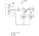
図13は、第3の変形例の配線オープン検出回路を示す回路図である。図13に示すように、配線オープン検出回路104は、ドライバDRIV1、配線MW1、端子PAD1、端子PAD1a、ダイオードD1、ダイオードD1a、テストバスTB、テストバスTBa、オープン判定回路1、オープン判定回路41を含む。配線オープン検出回路104は、第1の実施形態の配線オープン検出回路100(図2参照)に端子PAD1a、ダイオードD1a、テストバスTBa、オープン判定回路41を追加したものである。以下、第1の実施形態と異なる部分のみ説明する。
FIG. 13 is a circuit diagram illustrating a wiring open detection circuit according to a third modification. As shown in FIG. 13, the wiring
ダイオードD1aは、カソードが端子PAD1に接続され、アノードが端子PAD1aに接続される。端子PAD1aは、ドライバDRIV1側の配置される端子PAD1に対して、接地電位Vss側に設けられる端子である。オープン判定回路41は、一端がテストバスTBaに接続され、他端がMOSトランジスタNMT1のソースに接続され、テストバスTBaを介して電極PAD1aに接続される。
The diode D1a has a cathode connected to the terminal PAD1 and an anode connected to the terminal PAD1a. The terminal PAD1a is a terminal provided on the ground potential Vss side with respect to the terminal PAD1 arranged on the driver DRIV1 side. The
オープン判定回路41は、配線のオープン試験のときに、テストバスTBaと端子PAD1aを介してダイオードD1aのアノードにダイオードD1aの順方向電圧以上の正の電圧を印加し、長距離の配線MW1に流れる電流Itestの変化を検知し、長距離の配線MW1がオープンであるか否かを判定する。
The
図14は、第4の変形例の配線オープン検出回路を示す回路図である。図14に示すように、配線オープン検出回路103aは、ドライバDRIV1、配線MW21、電極DNK11〜DNK14、電極DNK21、電極DNK22、ビアVIA11〜VIA14、ダイオードD41〜D43、テストバスTB31〜TB33、オープン判定回路51を含む。配線オープン検出回路103aは、第4の実施形態の配線オープン検出回路103を変更及び追加したものである。
FIG. 14 is a circuit diagram illustrating a wiring open detection circuit according to a fourth modification. As shown in FIG. 14, the wiring
ドライバDRIV1、配線MW21、電極DNK11〜DNK14、ダイオードD41〜D43、テストバスTB31〜TB33、オープン判定回路51は、ドライバアレイチップに含まれる。電極DNK21、電極DNK22は、MEMSアレイチップに含まれる。
The driver DRIV1, the wiring MW21, the electrodes DNK11 to DNK14, the diodes D41 to D43, the test buses TB31 to TB33, and the
配線MW21は、一端がドライバDRIV1に接続され、他端が電極DNK11に接続される。電極DNK12は、電極DNK11に隣接配置され、例えば電極DNK11と同じ層に形成される接地電位Vss側の電極である。電極DNK13は、電極DNK12に隣接配置され、例えば電極DNK11と同じ層に形成される接地電位Vss側の電極である。電極DNK14は、電極DNK13に隣接配置され、例えば電極DNK11と同じ層に形成される電極である。 The wiring MW21 has one end connected to the driver DRIV1 and the other end connected to the electrode DNK11. The electrode DNK12 is disposed adjacent to the electrode DNK11 and is, for example, an electrode on the ground potential Vss side formed in the same layer as the electrode DNK11. The electrode DNK13 is disposed adjacent to the electrode DNK12 and is, for example, an electrode on the ground potential Vss side formed in the same layer as the electrode DNK11. The electrode DNK14 is an electrode arranged adjacent to the electrode DNK13 and formed on the same layer as the electrode DNK11, for example.
電極DNK21は、一端がビアVIA11を介して電極DNK11に接続され、他端がビアVIA12を介して電極DNK12に接続されるMEMS電極である。電極DNK22は、一端がビアVIA14を介して電極DNK14に接続され、他端がビアVIA13を介して電極DNK13に接続されるMEMSの接地電位Vss側電極である。 The electrode DNK21 is a MEMS electrode having one end connected to the electrode DNK11 via the via VIA11 and the other end connected to the electrode DNK12 via the via VIA12. The electrode DNK22 is a ground potential Vss-side electrode of MEMS having one end connected to the electrode DNK14 via the via VIA14 and the other end connected to the electrode DNK13 via the via VIA13.
ダイオードD41は、カソードが電極DNK11に接続され、他端がテストバスTB31に接続される。ダイオードD42は、カソードが電極DNK12に接続され、アノードが電極DNK13に接続される。ダイオードD43は、カソードが電極DNK11に接続され、アノードが電極DNK14に接続される。 The diode D41 has a cathode connected to the electrode DNK11 and the other end connected to the test bus TB31. The diode D42 has a cathode connected to the electrode DNK12 and an anode connected to the electrode DNK13. The diode D43 has a cathode connected to the electrode DNK11 and an anode connected to the electrode DNK14.
テストバスTB32は、一端が電極DNK14に接続される。テストバスTB33は、一端が電極DNK14に接続され、他端がオープン判定回路51に接続される。
One end of the test bus TB32 is connected to the electrode DNK14. The test bus TB33 has one end connected to the electrode DNK14 and the other end connected to the
オープン判定回路51は、一端がテストバスTB33に接続され、他端がMOSトランジスタNMT1のソースに接続されている。
The
配線オープン検出回路103aの配線オープン試験での印加電圧は、図15Aに示すように、ドライバアレイとMEMSアレイの通常動作のとき、オープン判定回路51は、ダイオードD41のアノードに接地電位Vssであるテストバス印加電圧Vtb1を印加し、ダイオードD43のアノードに接地電位Vssであるテストバス印加電圧Vtb2を印加し、ダイオードD42のアノードに接地電位Vssであるテストバス印加電圧Vtb3を印加する。
As shown in FIG. 15A, when the normal operation of the driver array and the MEMS array is performed, the applied voltage in the wire open test of the wire
配線オープン検出回路103aの配線オープン試験のとき、オープン判定回路51は、テストバスTB33、電極DNK14、ビアVIA14、電極DNK22、ビアVIA13、及び電極DNK13を介してダイオードD42のアノードにダイオードD42の順方向電圧よりも大きな正の電圧であるテストバス印加電圧Vtb3を印加する。このとき、テストバス印加電圧Vtb1とテストバス印加電圧Vtb2は、接地電位Vssに設定される。
At the time of the wiring open test of the wiring
オープン判定回路51は、配線オープン試験のときに、テストバスTB33〜電極DNK14〜ビアVIA14〜電極DNK22〜ビアVIA13〜電極DNK13〜ダイオードD42〜電極DNK12〜ビアVIA12〜電極DNK21〜ビアVIA11〜電極DNK11を介して長距離の配線MW21に流れる電流Itestを検知して、長距離の配線MW21がオープンであるか否かを判定する。
The open determining
本発明のいくつかの実施形態を説明したが、これらの実施形態は、例として提示したものであり、発明の範囲を限定することは意図していない。これら新規な実施形態は、その他の様々な形態で実施されることが可能であり、発明の要旨を逸脱しない範囲で、種々の省略、置き換え、変更を行うことができる。これら実施形態やその変形は、発明の範囲や要旨に含まれるとともに、特許請求の範囲に記載された発明とその均等の範囲に含まれる。 While some embodiments of the invention have been described, these embodiments have been presented by way of example only, and are not intended to limit the scope of the inventions. These new embodiments can be implemented in other various forms, and various omissions, replacements, and changes can be made without departing from the spirit of the invention. These embodiments and their modifications are included in the scope and gist of the invention, and are also included in the invention described in the claims and their equivalents.
本発明は、以下の付記に記載されているような構成が考えられる。
(付記1)
第1配線の一端に接続され、信号処理した信号を前記第1配線に出力する信号処理回路と、
前記第1配線の他端に接続される第1電極と、
第1ビアを介して前記第1電極に接続され、前記第1電極よりも上層の第2電極と、
前記第1電極と同一層に形成され、第2のビアを介して前記第2電極に接続される第3電極と、
一端が前記第3電極に接続されるダイオードと、
一端が前記ダイオードの他端に接続されるテストバスと、
前記テストバスの他端に接続され、前記テストバスを介して前記ダイオードの他端に第1電圧を印加し、前記第1配線に流れる電流の変化を検出して前記第3電極から前記第1配線までの配線がオープンか否かを判定するオープン判定回路と、
を有する配線オープン検出回路。
The present invention may be configured as described in the following supplementary notes.
(Appendix 1)
A signal processing circuit that is connected to one end of the first wiring and outputs a signal after signal processing to the first wiring;
A first electrode connected to the other end of the first wiring;
A second electrode connected to the first electrode via a first via and being a layer above the first electrode;
A third electrode formed on the same layer as the first electrode and connected to the second electrode via a second via;
A diode having one end connected to the third electrode;
A test bus having one end connected to the other end of the diode;
A first voltage is connected to the other end of the test bus, a first voltage is applied to the other end of the diode via the test bus, a change in current flowing through the first wiring is detected, and the first electrode is connected to the first electrode. An open determination circuit that determines whether the wiring up to the wiring is open;
A wiring open detection circuit having
(付記2)
第1配線の一端に接続され、信号処理した信号を前記第1配線に出力する信号処理回路と、
前記第1配線の他端に接続される第1電極と、
第1ビアを介して前記第1電極に接続され、前記第1電極よりも上層の第2電極と、
前記第1電極と同一層に形成され、第2のビアを介して前記第2電極に接続される第3電極と、
前記第1電極と同一層に形成される第4電極と、
第3ビアを介して前記第4電極に接続され、前記第4電極よりも上層の第5電極と、
前記第4電極と同一層に形成され、第4のビアを介して前記第5電極に接続される第6電極と、
一端が前記第3電極に接続され、他端が前記第6電極に接続されるダイオードと、
一端が前記第4電極に接続されるテストバスと、
前記テストバスの他端に接続され、前記テストバスを介して前記ダイオードの他端に第1電圧を印加し、前記第4電極から前記第1配線に流れる電流の変化を検出して前記第4電極から前記第1配線までの配線がオープンか否かを判定するオープン判定回路と、
を有する配線オープン検出回路。
(Appendix 2)
A signal processing circuit that is connected to one end of the first wiring and outputs a signal after signal processing to the first wiring;
A first electrode connected to the other end of the first wiring;
A second electrode connected to the first electrode via a first via and being a layer above the first electrode;
A third electrode formed on the same layer as the first electrode and connected to the second electrode via a second via;
A fourth electrode formed on the same layer as the first electrode;
A fifth electrode connected to the fourth electrode via a third via, and located above the fourth electrode;
A sixth electrode formed on the same layer as the fourth electrode and connected to the fifth electrode via a fourth via;
A diode having one end connected to the third electrode and the other end connected to the sixth electrode;
A test bus having one end connected to the fourth electrode;
The fourth terminal is connected to the other end of the test bus, applies a first voltage to the other end of the diode via the test bus, detects a change in current flowing from the fourth electrode to the first wiring, and An open determination circuit that determines whether a wiring from an electrode to the first wiring is open;
A wiring open detection circuit having
1、1a、1b、11a、11b、21、31、41、51 オープン判定回路
2 アナログ・デジタルコンバータ
100〜104、100a、101a、103a 配線オープン検出回路
BUFF1、BUFF2 バッファ
C1〜C4、Cn−1、Cn キャパシタ
ChipA、ChipB 集積回路チップ
D1〜D4、Dn−1、Dn、D11、D12、D21、D22、D31〜D34、D3n−1、D3n、D1a、D41〜D43 ダイオード
DNK1〜DNK3、DNK11〜DNK14、DNK21、DNK22 電極
DRIV1〜DRIV4、DRIVn−1、DRIVn ドライバ
Itest 電流
NMT1、NMT11,NMT12 MOSトランジスタ
MW1〜MW4、MWn−1、MWn、MW11、MW21 配線
PAD1〜PAD4、PADn−1、PADn、PAD11〜PAD14、PAD1a 端子
PMT1、PMT11、PMT12 MOSトランジスタ
R1〜R4、Rn−1、Rn 抵抗
Sin 入力信号
Sout 出力信号
SW1、SW2 スイッチ
TB、TB1、TB2、TB11、TB12、TB21、TB22,TBa、TB31〜TB33 テストバス
VDD1 電源(高電位側電源)
VIA1、VIA2、VIA11〜VIA14 ビア
Vss 接地電位(低電位側電源)
Vtb、Vtb1、Vtb2、Vtb3 テストバス印加電圧
1, 1a, 1b, 11a, 11b, 21, 31, 41, 51 Open determination circuit 2 Analog /
VIA1, VIA2, VIA11 to VIA14 Via Vss Ground potential (low-potential side power supply)
Vtb, Vtb1, Vtb2, Vtb3 Test bus applied voltage
Claims (8)
前記第1配線の他端に接続される端子と、
一端が前記端子に接続されるダイオードと、
一端が前記ダイオードの他端に接続されるテストバスと、
前記テストバスの他端に接続され、前記テストバスを介して前記ダイオードの他端に第1電圧を印加し、前記第1配線に流れる電流の変化を検出して前記第1配線がオープンか否かを判定するオープン判定回路と、
を具備することを特徴とする配線オープン検出回路。 A signal processing circuit that is connected to one end of the first wiring and outputs a signal after signal processing to the first wiring;
A terminal connected to the other end of the first wiring;
A diode having one end connected to the terminal;
A test bus having one end connected to the other end of the diode;
A first voltage is connected to the other end of the test bus, a first voltage is applied to the other end of the diode via the test bus, and a change in a current flowing through the first wiring is detected to determine whether the first wiring is open. An open determination circuit for determining whether
A wiring open detection circuit, comprising:
前記第1電圧は、前記ダイオードの順方向電圧よりも大きな正の電圧である
ことを特徴とする請求項1に記載の配線オープン検出回路。 One end of the diode is a cathode, the other end of the diode is an anode,
The wiring open detection circuit according to claim 1, wherein the first voltage is a positive voltage larger than a forward voltage of the diode.
前記第1電圧は、前記ダイオードの耐圧よりも大きな正の電圧である
ことを特徴とする請求項1に記載の配線オープン検出回路。 One end of the diode is an anode, the other end of the diode is a cathode,
The wiring open detection circuit according to claim 1, wherein the first voltage is a positive voltage larger than a withstand voltage of the diode.
前記第1配線の他端に接続される端子と、
一端が前記端子に接続される、前記信号処理回路から出力される信号により電荷を蓄積するキャパシタと、
一端が前記キャパシタの他端に接続されるテストバスと、
前記テストバスの他端に接続され、前記テストバスを介して前記キャパシタから放電される蓄積電荷の変化を検出して前記第1配線がオープンか否かを判定するオープン判定回路と、
を具備することを特徴とする配線オープン検出回路。 A signal processing circuit that is connected to one end of the first wiring and outputs a signal after signal processing to the first wiring;
A terminal connected to the other end of the first wiring;
One end is connected to the terminal, a capacitor that accumulates charge by a signal output from the signal processing circuit,
A test bus having one end connected to the other end of the capacitor;
An open determination circuit that is connected to the other end of the test bus and detects a change in accumulated charge discharged from the capacitor via the test bus to determine whether the first wiring is open;
A wiring open detection circuit, comprising:
前記アナログ・デジタルコンバータは、前記キャパシタから放電される電荷をアナログ信号として入力し、アナログ・デジタル変換した信号を出力し、
前記オープン判定回路は、前記アナログ・デジタルコンバータの出力信号が接地電位レベルを維持するときは前記第1配線がオープンであると判定し、前記アナログ・デジタルコンバータの出力信号レベルが変化する場合は前記第1配線が正常であると判定する、
ことを特徴とする請求項4に記載の配線オープン検出回路。 The open determination circuit includes an analog-to-digital converter,
The analog-to-digital converter inputs a charge discharged from the capacitor as an analog signal, and outputs a signal obtained by analog-to-digital conversion,
The open determination circuit determines that the first wiring is open when the output signal of the analog / digital converter maintains the ground potential level, and determines that the output signal of the analog / digital converter changes when the output signal level of the analog / digital converter changes. Determining that the first wiring is normal;
The wiring open detection circuit according to claim 4, wherein:
ことを特徴とする請求項4又は5に記載の配線オープン検出回路。 The wiring open detection circuit according to claim 4 or 5, wherein the capacitor is a capacitance between wirings or a gate capacitance formed between the terminal and the test bus.
第3端子と、前記第3端子に接続される信号処理回路と、一端が前記信号処理回路に接続され第2テストバスと、前記第2テストバスの他端に接続される第4端子とを有する第2集積回路チップと、
一端が前記第2端子に接続され、他端が前記第3端子に接続され、前記第1集積回路チップと前記第2集積回路チップの間を電気的に接続する第1配線と、
前記第1端子に第1電圧を印加し、前記第2テストバスを介して前記第4端子から出力される電流の変化を検出して前記第1配線がオープンか否かを判定するオープン判定回路と、
を具備することを特徴とする配線オープン検出回路。 A first terminal, a first test bus having one end connected to the first terminal, a first protection diode having one end connected to the other end of the first test bus, and a second end connected to the other end of the first diode; A first integrated circuit chip having a second terminal,
A third terminal, a signal processing circuit connected to the third terminal, a second test bus having one end connected to the signal processing circuit, and a fourth terminal connected to the other end of the second test bus. A second integrated circuit chip having
A first wiring having one end connected to the second terminal, the other end connected to the third terminal, and electrically connecting the first integrated circuit chip and the second integrated circuit chip;
An open determination circuit that applies a first voltage to the first terminal, detects a change in a current output from the fourth terminal via the second test bus, and determines whether the first wiring is open. When,
A wiring open detection circuit, comprising:
前記第1配線の他端に接続される端子と、
一端が前記端子に接続される高抵抗値を有する第1抵抗と、
一端が前記第1抵抗の他端に接続されるテストバスと、
前記テストバスの他端に接続され、前記テストバスを介して前記第1抵抗の他端に第1電圧を印加し、前記第1配線に流れる電流の変化を検出して前記第1配線がオープンか否かを判定するオープン判定回路と、
を具備することを特徴とする配線オープン検出回路。 A signal processing circuit that is connected to one end of the first wiring and outputs a signal after signal processing to the first wiring;
A terminal connected to the other end of the first wiring;
A first resistor having one end connected to the terminal and having a high resistance value;
A test bus having one end connected to the other end of the first resistor;
The first wiring is connected to the other end of the test bus, applies a first voltage to the other end of the first resistor via the test bus, detects a change in current flowing in the first wiring, and opens the first wiring. An open determination circuit for determining whether or not
A wiring open detection circuit, comprising:
Priority Applications (2)
| Application Number | Priority Date | Filing Date | Title |
|---|---|---|---|
| JP2018130394A JP7241482B2 (en) | 2018-07-10 | 2018-07-10 | Wiring open detection circuit |
| US16/266,135 US10942225B2 (en) | 2018-07-10 | 2019-02-04 | Wiring open detection circuit |
Applications Claiming Priority (1)
| Application Number | Priority Date | Filing Date | Title |
|---|---|---|---|
| JP2018130394A JP7241482B2 (en) | 2018-07-10 | 2018-07-10 | Wiring open detection circuit |
Publications (2)
| Publication Number | Publication Date |
|---|---|
| JP2020008444A true JP2020008444A (en) | 2020-01-16 |
| JP7241482B2 JP7241482B2 (en) | 2023-03-17 |
Family
ID=69140234
Family Applications (1)
| Application Number | Title | Priority Date | Filing Date |
|---|---|---|---|
| JP2018130394A Active JP7241482B2 (en) | 2018-07-10 | 2018-07-10 | Wiring open detection circuit |
Country Status (2)
| Country | Link |
|---|---|
| US (1) | US10942225B2 (en) |
| JP (1) | JP7241482B2 (en) |
Citations (9)
| Publication number | Priority date | Publication date | Assignee | Title |
|---|---|---|---|---|
| JPH03225233A (en) * | 1990-01-31 | 1991-10-04 | Hitachi Ltd | Burnout circuit for 3-wire resistor under test |
| JP2001296330A (en) * | 2000-04-11 | 2001-10-26 | Fujitsu Ltd | Electronic device having disconnection position detection function and disconnection position detection method |
| JP2003029296A (en) * | 2001-07-13 | 2003-01-29 | Toshiba Corp | Array substrate, inspection method therefor, and liquid crystal display device |
| JP2005017099A (en) * | 2003-06-26 | 2005-01-20 | Renesas Technology Corp | Multi-chip module |
| JP2007147330A (en) * | 2005-11-24 | 2007-06-14 | Fujifilm Corp | Semiconductor chip and test method thereof |
| US20110204910A1 (en) * | 2008-11-14 | 2011-08-25 | Teradyne, Inc. | Method and apparatus for testing electrical connections on a printed circuit board |
| JP2012042226A (en) * | 2010-08-12 | 2012-03-01 | Rohm Co Ltd | Semiconductor device and testing method thereof |
| JP2012127803A (en) * | 2010-12-15 | 2012-07-05 | Denso Corp | Semiconductor integrated circuit |
| JP2014095687A (en) * | 2012-10-12 | 2014-05-22 | Institute Of National Colleges Of Technology Japan | Solder connection part test circuit and method |
Family Cites Families (7)
| Publication number | Priority date | Publication date | Assignee | Title |
|---|---|---|---|---|
| US4056773A (en) * | 1976-08-25 | 1977-11-01 | Sullivan Donald F | Printed circuit board open circuit tester |
| US5124660A (en) * | 1990-12-20 | 1992-06-23 | Hewlett-Packard Company | Identification of pin-open faults by capacitive coupling through the integrated circuit package |
| US6614253B2 (en) * | 2001-08-03 | 2003-09-02 | Northrop Grumman Corporation | On-circuit board continuity tester |
| US7030623B1 (en) * | 2004-02-03 | 2006-04-18 | Kevin Carpenter | Electrical short tracing apparatus and method |
| JP4337983B2 (en) | 2005-02-17 | 2009-09-30 | 国立大学法人 東京大学 | Mixed semiconductor integrated circuit and manufacturing method thereof |
| JP2010221372A (en) | 2009-03-25 | 2010-10-07 | Seiko Epson Corp | MEMS device and inspection method thereof |
| US8970237B2 (en) * | 2012-05-07 | 2015-03-03 | Tesla Motors, Inc. | Wire break detection in redundant communications |
-
2018
- 2018-07-10 JP JP2018130394A patent/JP7241482B2/en active Active
-
2019
- 2019-02-04 US US16/266,135 patent/US10942225B2/en active Active
Patent Citations (9)
| Publication number | Priority date | Publication date | Assignee | Title |
|---|---|---|---|---|
| JPH03225233A (en) * | 1990-01-31 | 1991-10-04 | Hitachi Ltd | Burnout circuit for 3-wire resistor under test |
| JP2001296330A (en) * | 2000-04-11 | 2001-10-26 | Fujitsu Ltd | Electronic device having disconnection position detection function and disconnection position detection method |
| JP2003029296A (en) * | 2001-07-13 | 2003-01-29 | Toshiba Corp | Array substrate, inspection method therefor, and liquid crystal display device |
| JP2005017099A (en) * | 2003-06-26 | 2005-01-20 | Renesas Technology Corp | Multi-chip module |
| JP2007147330A (en) * | 2005-11-24 | 2007-06-14 | Fujifilm Corp | Semiconductor chip and test method thereof |
| US20110204910A1 (en) * | 2008-11-14 | 2011-08-25 | Teradyne, Inc. | Method and apparatus for testing electrical connections on a printed circuit board |
| JP2012042226A (en) * | 2010-08-12 | 2012-03-01 | Rohm Co Ltd | Semiconductor device and testing method thereof |
| JP2012127803A (en) * | 2010-12-15 | 2012-07-05 | Denso Corp | Semiconductor integrated circuit |
| JP2014095687A (en) * | 2012-10-12 | 2014-05-22 | Institute Of National Colleges Of Technology Japan | Solder connection part test circuit and method |
Also Published As
| Publication number | Publication date |
|---|---|
| US20200018788A1 (en) | 2020-01-16 |
| US10942225B2 (en) | 2021-03-09 |
| JP7241482B2 (en) | 2023-03-17 |
Similar Documents
| Publication | Publication Date | Title |
|---|---|---|
| US9473133B2 (en) | Control device | |
| US6885212B2 (en) | Semiconductor device and test method for the same | |
| US8139330B2 (en) | Semiconductor integrated circuit | |
| US9076656B2 (en) | Electrostatic discharge (ESD) clamp circuit with high effective holding voltage | |
| US7352547B2 (en) | Semiconductor integrated circuit device | |
| US20060255827A1 (en) | Inspection method and inspection device for display device and active matrix substrate used for display device | |
| US8879220B2 (en) | Electrostatic discharge protection circuit | |
| US10193538B2 (en) | Semiconductor device | |
| US20090067106A1 (en) | Static electricity discharge circuit | |
| JP2017022830A (en) | Power converter | |
| US9553446B2 (en) | Shared ESD circuitry | |
| CN107393842B (en) | Semiconductor device, semiconductor chip, and method for testing semiconductor chip | |
| US20080198520A1 (en) | Electrostatic discharge protection circuit with lowered driving voltage | |
| JP2009047473A (en) | Semiconductor device | |
| JP7241482B2 (en) | Wiring open detection circuit | |
| EP3477317B1 (en) | Method for identifying a fault at a device output and system therefor | |
| JP2012194183A (en) | Semiconductor device | |
| US12580558B2 (en) | Device, half bridge and method for operating a device | |
| JP5219342B2 (en) | Method and arrangement for ESD protection of AC coupled locations | |
| JP2018182997A (en) | Semiconductor device and control method thereof | |
| JP4321161B2 (en) | Semiconductor device evaluation method | |
| CN118974940A (en) | Semiconductor devices | |
| CN115372807A (en) | Signal detection circuit | |
| JP2011040521A (en) | Protective circuit | |
| JP5196222B2 (en) | Gate breakdown voltage testing apparatus and method |
Legal Events
| Date | Code | Title | Description |
|---|---|---|---|
| A621 | Written request for application examination |
Free format text: JAPANESE INTERMEDIATE CODE: A621 Effective date: 20201125 |
|
| A977 | Report on retrieval |
Free format text: JAPANESE INTERMEDIATE CODE: A971007 Effective date: 20211029 |
|
| A131 | Notification of reasons for refusal |
Free format text: JAPANESE INTERMEDIATE CODE: A131 Effective date: 20211102 |
|
| RD01 | Notification of change of attorney |
Free format text: JAPANESE INTERMEDIATE CODE: A7421 Effective date: 20211221 |
|
| A603 | Late request for extension of time limit during examination |
Free format text: JAPANESE INTERMEDIATE CODE: A603 Effective date: 20220125 |
|
| A521 | Request for written amendment filed |
Free format text: JAPANESE INTERMEDIATE CODE: A523 Effective date: 20220202 |
|
| A131 | Notification of reasons for refusal |
Free format text: JAPANESE INTERMEDIATE CODE: A131 Effective date: 20220510 |
|
| A521 | Request for written amendment filed |
Free format text: JAPANESE INTERMEDIATE CODE: A523 Effective date: 20220610 |
|
| A131 | Notification of reasons for refusal |
Free format text: JAPANESE INTERMEDIATE CODE: A131 Effective date: 20221003 |
|
| A521 | Request for written amendment filed |
Free format text: JAPANESE INTERMEDIATE CODE: A523 Effective date: 20221111 |
|
| TRDD | Decision of grant or rejection written | ||
| A01 | Written decision to grant a patent or to grant a registration (utility model) |
Free format text: JAPANESE INTERMEDIATE CODE: A01 Effective date: 20230206 |
|
| A61 | First payment of annual fees (during grant procedure) |
Free format text: JAPANESE INTERMEDIATE CODE: A61 Effective date: 20230307 |
|
| R150 | Certificate of patent or registration of utility model |
Ref document number: 7241482 Country of ref document: JP Free format text: JAPANESE INTERMEDIATE CODE: R150 |