JP2020008790A - Cover film, display having the same, manufacturing method of cover film, and manufacturing method of display - Google Patents
Cover film, display having the same, manufacturing method of cover film, and manufacturing method of display Download PDFInfo
- Publication number
- JP2020008790A JP2020008790A JP2018131863A JP2018131863A JP2020008790A JP 2020008790 A JP2020008790 A JP 2020008790A JP 2018131863 A JP2018131863 A JP 2018131863A JP 2018131863 A JP2018131863 A JP 2018131863A JP 2020008790 A JP2020008790 A JP 2020008790A
- Authority
- JP
- Japan
- Prior art keywords
- film
- decorative layer
- optical film
- display
- cover film
- Prior art date
- Legal status (The legal status is an assumption and is not a legal conclusion. Google has not performed a legal analysis and makes no representation as to the accuracy of the status listed.)
- Pending
Links
Images


Landscapes
- Liquid Crystal (AREA)
- Electroluminescent Light Sources (AREA)
- Devices For Indicating Variable Information By Combining Individual Elements (AREA)
Abstract
Description
本発明は、カバーフィルム、そのカバーフィルムを備えたディスプレイ、カバーフィルムの製造方法およびディスプレイの製造方法に関するものである。 The present invention relates to a cover film, a display provided with the cover film, a method for manufacturing a cover film, and a method for manufacturing a display.
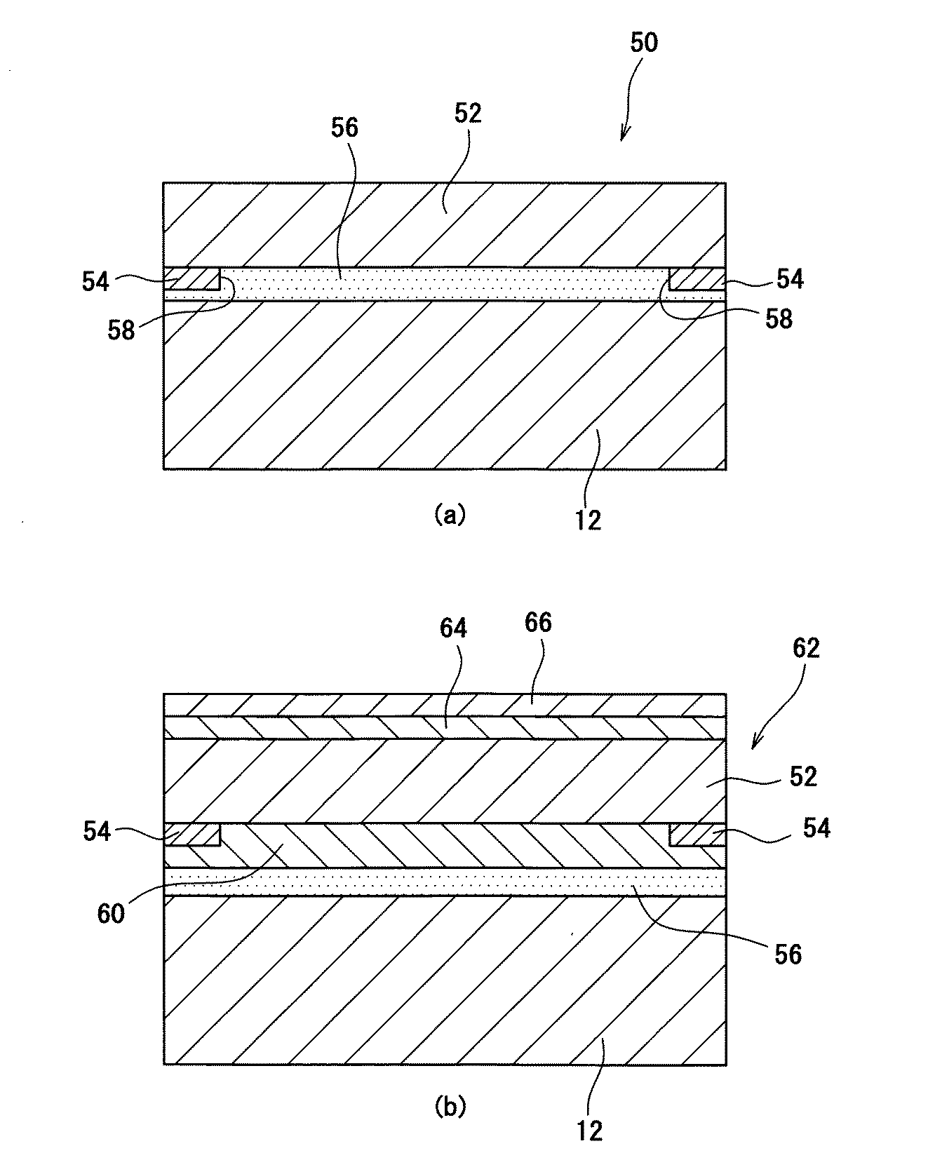
従来、図5(a)に示すように、ディスプレイ12の前面にカバーフィルム50が張り付けられている。そのカバーフィルム50は、透明のPETフィルム52およびそのPETフィルム52の外周部に積層した加飾層54を備えている。カバーフィルム50は光学透明接着剤56を介してディスプレイ12の前面に張り付けられている。加飾層54は不透明であり、ディスプレイ12の外周部の配線を隠している。
Conventionally, as shown in FIG. 5A, a
図5(a)の構成の場合、PETフィルム52と加飾層54とで光学透明接着剤56に段差58が生じている。光学透明接着剤56における段差付近に気泡が生じる場合がある。その対策として、PETフィルム52と加飾層54を覆うように紫外線硬化樹脂層60を形成したカバーフィルム62が下記特許文献1に開示されている(図5(b))。紫外線硬化樹脂層60がディスプレイ12に張り付けられるため、光学透明接着剤56に段差がなく、光学透明接着剤56に気泡が生じない。なお、特許文献1はハードコート層64や保護層66を設けているが、図5(a)の場合も同じようにそれらの層64、66を設けてもよい。
In the case of the configuration shown in FIG. 5A, a
しかし、PETフィルム52と加飾層54を紫外線硬化樹脂層60で覆うため、カバーフィルム62が厚くなる。そのため、カバーフィルム62がディスプレイ12の薄型化の妨げになる。
However, since the PET
本発明の目的は、ディスプレイの薄型化が可能なカバーフィルム、そのカバーフィルムを備えたディスプレイ、カバーフィルムの製造方法およびディスプレイの製造方法を提供することにある。 An object of the present invention is to provide a cover film capable of reducing the thickness of a display, a display including the cover film, a method of manufacturing a cover film, and a method of manufacturing a display.
本発明のカバーフィルムは、中央部と外周部を備え、外周部の厚みが中央部の厚みよりも薄い光学フィルムと、前記光学フィルムの外周部に形成され、該光学フィルムとで面一になった加飾層とで構成される。カバーフィルムはディスプレイの前面に配置される。 The cover film of the present invention includes a central portion and an outer peripheral portion, and the outer peripheral portion has a thickness smaller than the thickness of the central portion, and is formed on the outer peripheral portion of the optical film and is flush with the optical film. And decorative layers. The cover film is disposed on the front of the display.
前記光学フィルムの鉛筆硬度がH以上であり、加飾層の鉛筆硬度がB以上である。また、前記光学フィルムの中央部の表面と加飾層の表面が同一の表面粗さである。さらに、前記光学フィルムが紫外線硬化樹脂または熱硬化性樹脂である。 The pencil hardness of the optical film is H or more, and the pencil hardness of the decorative layer is B or more. Further, the surface of the central portion of the optical film and the surface of the decorative layer have the same surface roughness. Further, the optical film is an ultraviolet curable resin or a thermosetting resin.
本発明のディスプレイは、上記カバーフィルムが前面に配置されている。 In the display of the present invention, the cover film is disposed on the front surface.
本発明のカバーフィルムの製造方法は、2枚のベースフィルムを準備する工程と、前記一のベースフィルムの一面に加飾層を形成する工程と、前記一のベースフィルムの一面および加飾層を光学フィルムの材料で覆った状態で、2枚のベースフィルムで光学フィルムの材料と加飾層を挟み込む工程と、前記光学フィルムの材料を硬化させて光学フィルムを形成する工程と、前記光学フィルムと加飾層を2枚のベースフィルムから剥がす工程とを備える。 The method for producing a cover film of the present invention includes a step of preparing two base films, a step of forming a decorative layer on one surface of the one base film, and a step of forming one surface and the decorative layer of the one base film. In the state covered with the optical film material, the step of sandwiching the optical film material and the decorative layer with two base films, the step of curing the optical film material to form an optical film, and the optical film; Peeling off the decorative layer from the two base films.
前記加飾層の接触角は一のベースフィルムの接触角よりも小さい。また、前記透明樹脂が紫外線硬化樹脂または熱硬化性樹脂であり、前記光学フィルムを形成する工程は、紫外線照射または加熱によって光学フィルムを形成する。 The contact angle of the decorative layer is smaller than the contact angle of one base film. Further, the transparent resin is an ultraviolet curable resin or a thermosetting resin, and in the step of forming the optical film, the optical film is formed by irradiation with ultraviolet light or heating.
前記カバーフィルムをディスプレイの前面に張り付けることによって、ディスプレイを製造する。 The display is manufactured by attaching the cover film to the front surface of the display.
本発明は、光学フィルムと加飾層からなるカバーフィルムであり、従来のようにPETフィルム上に加飾層の段差を形成していない。そのため、本発明のカバーフィルムとディスプレイは薄型化が可能である。さらに、カバーフィルムとディスプレイの間の光学透明接着剤に段差を生じさせないので、光学透明接着剤に気泡を生じさせることもない。 The present invention is a cover film including an optical film and a decorative layer, and does not form a step of the decorative layer on the PET film as in the related art. Therefore, the cover film and the display of the present invention can be made thin. Further, since no step is generated in the optical transparent adhesive between the cover film and the display, no bubbles are generated in the optical transparent adhesive.
本発明のカバーフィルム、そのカバーフィルムを備えたディスプレイ、カバーフィルムの製造方法およびディスプレイの製造方法について図面を用いて説明する。図面は模式的に示しており、説明の便宜上、図面によって大きさの異なる場合がある。 The cover film of the present invention, a display including the cover film, a method of manufacturing the cover film, and a method of manufacturing the display will be described with reference to the drawings. The drawings are schematically shown, and for convenience of description, the sizes may be different depending on the drawings.
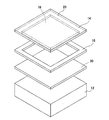
図1、図2に示すカバーフィルム10は、ディスプレイ12の前面に配置されるものである。カバーフィルム10は、光学フィルム14および加飾層16で構成される。
The
(光学フィルム)
光学フィルム14はシート状または薄膜状になっており、中央部18と外周部20を備える。図1の光学フィルム14はディスプレイ12の前面の外形形状と同じ形状になっているが、異なる形状になっていてもよい。ディスプレイ12における表示部分22の上に配置される部分が中央部18であり、表示部分22の周辺部24の上に配置される部分が外周部20である。
(Optical film)
The
光学フィルム14の一面26において、中央部18に対して外周部20が窪んでいる。このため、外周部20の厚みは中央部18の厚みよりも薄くなっている。光学フィルム14の厚みは、中央部18で約20〜300μm、好ましくは50〜200μm、より好ましくは75〜150μmである。さらに外周部20の厚みは約10〜295μm、好ましくは40〜195μm、より好ましくは60〜145μmであり、外周部20の厚みが中央部18の厚みよりも薄くなるように選択される。
On one
光学フィルム14はディスプレイ12の表示部分22が視認できるように透明である。光学フィルム14の材料は紫外線硬化樹脂(電離放射線硬化型樹脂)である。紫外線硬化樹脂の前駆体材料としては、メタクリロイル基、アクリロイル基を合計で3以上有する多官能(メタ)アクリレートを含むことが好ましい。多官能(メタ)アクリレートの(メタ)アクリロイル基以外の骨格構造は特に限定されず、たとえばシリコーン系、ウレタン系、エポキシ系、フッ素系、脂肪族系の骨格構造を有するものを用いることができる。
The
表面硬度が高く且つ可撓性があって割れにくいシートまたは薄膜を作製できることから、(メタ)アクリロイル基を有する有機官能基がケイ素に結合した篭型ポリオルガノシルセスキオキサンを主成分とする多官能のシリコーン系樹脂を用いることが好ましい。また、シリコーン系樹脂に代えて、多官能のウレタン系(メタ)アクリレート及び/又は多官能の脂肪族系(メタ)アクリレートを含有する重合性組成物を用いてもよい。さらに、シリコーン系樹脂に、上記のウレタン系(メタ)アクリレート及び/又は(メタ)アクリレートを混合してもよい。たとえば、シリコーン系樹脂100重量部に対して、100〜500重量部、好ましくは200〜400重量部のウレタン系(メタ)アクリレート及び/又は脂肪族系(メタ)系アクリレートを混合して用いることができる。 Since a sheet or a thin film having a high surface hardness and being flexible and resistant to cracking can be produced, a cage-type polyorganosilsesquioxane in which an organic functional group having a (meth) acryloyl group is bonded to silicon is used as a main component. It is preferable to use a functional silicone resin. Further, instead of the silicone-based resin, a polymerizable composition containing a polyfunctional urethane (meth) acrylate and / or a polyfunctional aliphatic (meth) acrylate may be used. Further, the urethane-based (meth) acrylate and / or (meth) acrylate may be mixed with the silicone-based resin. For example, 100 to 500 parts by weight, preferably 200 to 400 parts by weight of a urethane-based (meth) acrylate and / or an aliphatic (meth) -based acrylate may be mixed and used with respect to 100 parts by weight of a silicone-based resin. it can.
ポリオルガノシルセスキオキサンは、3官能性シランを加水分解することで得られる(RSiO1.5)nの構造を持つ化合物であり、本発明では、ポリオルガノシルセスキオキサンうち、篭型構造を有するものを用いることが好ましい。つまり、篭型ポリオルガノシルセスキオキサンは、その各シリコン(Si)原子が、平均1.5個の酸素(O)原子と1つの炭化水素基(R)と結合し、有機官能基とSi−O結合で出来たカゴ状骨格を有しているものである。このような構造であることで、硬化後の光学フィルムの硬度を高めるとともに、篭型ポリオルガノシルセスキオキサンは、ケイ素(Si)原子の数(上記n)が8、10、12であることが好ましい。 The polyorganosilsesquioxane is a compound having a structure of (RSiO 1.5 ) n obtained by hydrolyzing a trifunctional silane. In the present invention, the polyorganosilsesquioxane has a cage-type structure. It is preferable to use one having That is, in the cage-type polyorganosilsesquioxane, each silicon (Si) atom is bonded to an average of 1.5 oxygen (O) atoms and one hydrocarbon group (R), and an organic functional group and Si It has a cage-like skeleton made of -O bonds. With such a structure, the hardness of the optical film after curing is increased, and the number of silicon (Si) atoms (the above n) of the cage-type polyorganosilsesquioxane is 8, 10, or 12. Is preferred.
ウレタン系(メタ)アクリレートは、ポリイソシアネート化合物と水酸基含有(メタ)アクリレートとを反応させてなることで、分子内のウレタン基の水素結合により適度な靭性を付与されて機械強度に優れるとともに、多官能であるので硬化して架橋構造を形成し、硬度が高い樹脂成形体を得ることができるため、好ましい。ウレタン系(メタ)アクリレートの数平均分子量は、200〜5000であることが好ましい。数平均分子量が200未満であると、硬化収縮が増大し、複屈折が発生しやすくなるおそれにある。数平均分子量が5000を超えると、架橋性が低下し、耐熱性が不十分となるおそれがある。 The urethane (meth) acrylate is obtained by reacting a polyisocyanate compound with a hydroxyl group-containing (meth) acrylate, thereby imparting appropriate toughness due to hydrogen bonding of urethane groups in the molecule, and is excellent in mechanical strength. It is preferable because it is functional and can be cured to form a crosslinked structure and obtain a resin molded body having high hardness. The number average molecular weight of the urethane (meth) acrylate is preferably from 200 to 5,000. When the number average molecular weight is less than 200, curing shrinkage increases, and birefringence may easily occur. If the number average molecular weight exceeds 5,000, crosslinkability may be reduced and heat resistance may be insufficient.
ポリイソシアネート化合物としては特に限定されず、例えば、脂肪族ポリイソシアネート、芳香族ポリイソシアネート、及び芳香脂肪族ポリイソシアネートが挙げられるが、黄変を抑制できる点で脂肪族ポリイソシアネートを用いることが好ましい。またポリイソシアネート化合物として、脂環構造を有しない化合物を用いると、特に表面硬度が優れた透明フィルム4を得ることができ、好ましい。脂肪族ポリイソシアネートとしては、トリメチレンジイソシアネート、テトラメチレンジイソシアネート、ヘキサメチレンジイソシアネート(HDI)、ペンタメチレンジイソシアネート、1,2−プロピレンジイソシアネート、2,3−ブチレンジイソシアネート、1,3−ブチレンジイソシアネート、ドデカメチレンジイソシアネート、2,4,4−トリメチルヘキサメチレンジイソシアネート、リジンイソシアネート、水添キシレンジイソシアネート、水添ジフェニルメタンジイソシアネート、1,3−ビス(ジイソシアネートメチル)シクロヘキサン、4,4'−ジシクロヘキシルメタンジイソシアネート等が挙げられる。 The polyisocyanate compound is not particularly limited, and examples thereof include aliphatic polyisocyanate, aromatic polyisocyanate, and araliphatic polyisocyanate. It is preferable to use aliphatic polyisocyanate from the viewpoint of suppressing yellowing. When a compound having no alicyclic structure is used as the polyisocyanate compound, a transparent film 4 having particularly excellent surface hardness can be obtained, which is preferable. Examples of the aliphatic polyisocyanate include trimethylene diisocyanate, tetramethylene diisocyanate, hexamethylene diisocyanate (HDI), pentamethylene diisocyanate, 1,2-propylene diisocyanate, 2,3-butylene diisocyanate, 1,3-butylene diisocyanate, dodecamethylene diisocyanate , 2,4,4-trimethylhexamethylene diisocyanate, lysine isocyanate, hydrogenated xylene diisocyanate, hydrogenated diphenylmethane diisocyanate, 1,3-bis (diisocyanatomethyl) cyclohexane, 4,4'-dicyclohexylmethane diisocyanate, and the like.
水酸基含有(メタ)アクリレートとしては、分子中に水酸基及び(メタ)アクリロイル基を有していれば限定されないが、例えば、2−ヒドロキシエチル(メタ)アクリレート、2−ヒドロキシプロピル(メタ)アクリレート、2−ヒドロキシブチル(メタ)アクリレート、2−ヒドロキシ−3−(メタ)アクリロイロキシプロピル(メタ)アクリレート、ペンタエリスリトールトリ(メタ)アクリレート、ジペンタエリスリトールペンタ(メタ)アクリレート、ジペンタエリスリトールトリ(メタ)アクリレート、トリペンタエリスリトールヘプタアクリレート等が挙げられる。特に分子中に脂環構造を有しないものを用いることが、樹脂成形体の表面硬度、及び色目変化の抑制の点で好ましい。 The hydroxyl group-containing (meth) acrylate is not limited as long as it has a hydroxyl group and a (meth) acryloyl group in the molecule. For example, 2-hydroxyethyl (meth) acrylate, 2-hydroxypropyl (meth) acrylate, -Hydroxybutyl (meth) acrylate, 2-hydroxy-3- (meth) acryloyloxypropyl (meth) acrylate, pentaerythritol tri (meth) acrylate, dipentaerythritol penta (meth) acrylate, dipentaerythritol tri (meth) Acrylate, tripentaerythritol heptaacrylate and the like. In particular, it is preferable to use a resin having no alicyclic structure in the molecule, in terms of the surface hardness of the resin molded product and the suppression of color change.
脂肪族系(メタ)アクリレートとしては、脂肪族多価アルコールの(メタ)アクリレートを用いることができ、たとえば1,3,5−トリス(メタクリロイルオキシメチル)シクロヘキサン、1,3,5−トリス(メタクリロイルオキシエチルオキシメチル)シクロヘキサンなどの3官能(メタ)アクリレートがあげられる。 As the aliphatic (meth) acrylate, (meth) acrylate of an aliphatic polyhydric alcohol can be used. For example, 1,3,5-tris (methacryloyloxymethyl) cyclohexane, 1,3,5-tris (methacryloyl) And trifunctional (meth) acrylates such as (oxyethyloxymethyl) cyclohexane.
(加飾層)
加飾層16は光学フィルム14の外周部20に形成されている。加飾層16の一面28と光学フィルム14の中央部18とで面一になっている。加飾層16は、一面28が露出するように光学フィルム14に埋め込まれた構造である。
(Decoration layer)
The
加飾層16は光を遮断することで、ディスプレイ12の外周部24に配置された配線を視認されなくする。加飾層16は有色材料を印刷したり、フォトリソグラフィーでパターニングしたりすることによって形成される。有色材料はインク材料が好適であり、そのインク材料として、ウレタン系樹脂、ビニル系樹脂、ポリエステル系樹脂、アクリル系樹脂、ポリオレフィン系樹脂、エポキシ系樹脂などから選択できる。インク材料の形成時、その主成分である樹脂は溶剤で溶解されている。さらにインク材料の中に顔料や添加材が含まれる。加飾層16の色は黒色系が挙げられ、光を透過させない材料が好ましいが、光を半透過させたり赤外線を透過させたりする材料であってもよい。加飾層16の色を複数色にして、文字や図形があしらわれた加飾層16であってもよい。
The
(表面硬度)
光学フィルム14の鉛筆硬度はH以上、加飾層16の鉛筆硬度はB以上である。これによって、カバーフィルム10のいずれの面が指やペンでタッチされても、傷つきにくい。
(surface hardness)
The pencil hardness of the
(表面粗さ)
光学フィルム14の一面26および加飾層16の表面28は同じ表面粗さになっている。これは、カバーフィルム10を製造するときに同一のフィルム上に形成した後に剥がすためである。さらに、光学フィルム14の他面27も一面26および加飾層16の表面28と同じ表面粗さになっていてもよい。
(Surface roughness)
One
(ディスプレイ)
本願のディスプレイ12は、表面にカバーフィルム10が配置されている。ディスプレイ12は、液晶ディスプレイや有機ELディスプレイなどである。ディスプレイ12とカバーフィルム10は光学透明接着剤(Optical Clear Adhesive)30で接着する。カバーフィルム10は両面が平面になっているため、いずれの面がディスプレイ12に接着されてもよい。必要に応じて、カバーフィルム10におけるディスプレイ12と反対側の面に反射防止膜などの光学機能層を形成してもよい。また、ディスプレイ12はタッチパネルを取り付けたディスプレイであってもよい。ディスプレイ12の上にタッチパネル、カバーフィルム10の順番で重ねる。ディスプレイ12とタッチパネルの配線を加飾層16で覆う。
(display)
The
光学透明接着剤30に従来のような段差が無く、従来のような気泡を生じさせない。カバーフィルム10は、従来のようにPETフィルム上に加飾層の段差を形成していないため、ディスプレイ12の薄型化の妨げになりにくい。
The optical
(カバーフィルムの製造方法)
次に、カバーフィルム10の製造方法について説明する。(1)第1ベースフィルムと第2ベースフィルムを準備する。各ベースフィルムはポリエチレンテレフタレート、ポリイミド、ポリエチレンナフタレート、ポリエーテルサルフォン、ポリエーテルエーテルケトン、ポリカーボネート、ポリスチレン、ポリアミド、アクリル樹脂、環状ポリオレフィン樹脂などの樹脂からなるフィルムである。各ベースフィルムは、表面に光沢または非光沢のいずれかの加工が施されていてもよい。
(Method of manufacturing cover film)
Next, a method for manufacturing the
光学フィルム14の材料および加飾層16の材料も準備する。光学フィルム14の材料として紫外線硬化樹脂を使用するのであれば、たとえば上述した光ラジカル重合を行う(メタ)アクリロイル基を有する化合物を準備する。また、加飾層16の材料においても、たとえば上述したウレタン系樹脂を用いた有色のインク材料を準備する。
A material for the
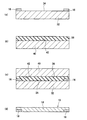
(2)第1ベースフィルム32の一面34の上に加飾層16を印刷形成する(図3(a))。たとえば、加飾層16をスクリーン印刷やインクジェット法などによって印刷形成する。
(2) The
(3)第1ベースフィルム32の一面34の露出部分と加飾層16の上に光学フィルム14の材料38を塗布する(図3(b))。コーターによって一定膜厚になるように材料38を塗布することが好ましい。
(3) The
(4)第2ベースフィルム40を光学フィルム14の材料38の上に配置し、2枚のベースフィルム32、40で加飾層16と材料38を挟み込む(図3(c))。光学フィルム14の材料38は第1ベースフィルム32における加飾層16の無い部分に接する。また、加飾層16は第2ベースフィルム40に接しない。光学フィルム14の材料38と加飾層16が所望の厚みになるように、一定間隔の2つのロールで第1ベースフィルム32から第2ベースフィルム40までの積層体を挟み込んでもよい。
(4) The
(5)光学フィルム14の材料38を硬化させて光学フィルム14を形成する。光学フィルム14が紫外線硬化樹脂を使用していれば紫外線を照射する。紫外線を照射する場合、加飾層16が紫外線を遮るため、加飾層16の無い方向または多方向から紫外線を照射することが好ましい。
(5) The
(6)第1ベースフィルム32と第2ベースフィルム40を光学フィルム14と加飾層16から剥がすことでカバーフィルム10が完成する(図3(d))。加飾層16の表面が露出した状態で、加飾層16が光学フィルム14に埋め込まれたようになっている。第1ベースフィルム32から加飾層16が剥がされるようにするため、第1ベースフィルム32の純水接触角よりも加飾層16の純水接触角を小さくする。また、光学フィルム14が第1および第2ベースフィルム32、40から剥がされるように、それらのベースフィルム32、40よりも純水接触角を小さくすることが好ましい。
(6) The
光学フィルム14と加飾層16が同じ第1ベースフィルム32の一面34に形成されたため、光学フィルム14の中央部18の表面と加飾層16の表面は同じ表面粗さである。第1ベースフィルム32と第2ベースフィルム40を同一の材料にすることで、光学フィルム14の中央部18の表面、その反対面、および加飾層16の表面が同じ表面粗さになる。光学フィルム14は第1ベースフィルム32の上に形成するため、光学フィルム14を薄く形成することができる。
Since the
上記工程において、第1ベースフィルム32と第2ベースフィルム40は長尺状のものを準備し、ロール・ツー・ロール(Roll to Roll)でおこなってもよい。第1ベースフィルム32と第2ベースフィルム40を移送させながら光学フィルム14と加飾層16を形成する。
In the above process, the
製造されたカバーフィルム10をディスプレイ12の表面に光学透明接着剤30を介して接着することで、本願のカバーフィルム10を備えたディスプレイ12を製造できる。図1では光学フィルム14の一面26と加飾層16の表面28がディスプレイ12に接着されているが、光学フィルム14の他面27がディスプレイ12に接着されていてもよい。
By bonding the manufactured
次に、本願の実施例として以下のようにカバーフィルム10を作成した。
(加飾層の形成)
離型性を有する平滑な第1ベースフィルム32(東洋紡株式会社製A4200)に、インク(セイコーアドバンス製HF GV3 710ブラック)をスクリーン印刷で加飾層16が印刷された第1ベースフィルム32を用意した(図3(a))。
Next, as an example of the present application, a
(Formation of decorative layer)
Prepare a
(光学フィルム前駆体の調製)
メタクリロイル基を全てのケイ素原子上に有した篭型ポリオルガノシルセスキオキサン:25重量部、トリメチロールプロパントリアクリレート:10重量部、ジシクロペンタニルジアクリレート:60重量部、ウレタンアクリレートオリゴマー1.5重量部、光重合開始剤としての1−ヒドロキシシクロヘキシルフェニルケトン:2.5重量部を混合し、光学フィルム前駆体(光学フィルムの材料38)を調製した。
(Preparation of optical film precursor)
Basket-type polyorganosilsesquioxane having methacryloyl groups on all silicon atoms: 25 parts by weight, trimethylolpropane triacrylate: 10 parts by weight, dicyclopentanyl diacrylate: 60 parts by weight, urethane acrylate oligomer 5 parts by weight and 2.5 parts by weight of 1-hydroxycyclohexylphenyl ketone as a photopolymerization initiator were mixed to prepare an optical film precursor (optical film material 38).
(積層体の作製)
得られた光学フィルム前駆体材料を、硬化後の膜厚が100μmとなるように、加飾層16が形成された第1ベースフィルム32の上にテスター産業株式会社製のバーコーター(ROD#75)を用いて塗布し、光学フィルム前駆体を形成した(図3(b))。さらに光学フィルム前駆体と第2ベースフィルム40(東洋紡株式会社製A4200)の一面42が接するように重ね合わせて、積層体を作製した(図3(c))。
(Preparation of laminate)
A bar coater (ROD # 75, manufactured by Tester Sangyo Co., Ltd.) is applied to the obtained optical film precursor material on the
(紫外線の照射(重合))
紫外線硬化装置(フュージョンUVシステムズ・ジャパン株式会社製:CV−110Q−G)を用いて、上記積層体に積算照射量1500mJ/cm2の紫外線を照射し、光学フィルム前駆体に含まれる未硬化の紫外線硬化樹脂を光ラジカル重合させた。
(UV irradiation (polymerization))
The above-mentioned laminate was irradiated with ultraviolet rays having an integrated irradiation amount of 1500 mJ / cm 2 using an ultraviolet curing device (manufactured by Fusion UV Systems Japan Co., Ltd .: CV-110Q-G), and the uncured uncured material contained in the optical film precursor was irradiated. The ultraviolet curable resin was subjected to photo-radical polymerization.
(剥離工程)
光ラジカル重合後の積層体の両面のベースフィルム32、40を剥離し、光学フィルム14に加飾層16を転写形成し、実施例にかかるカバーフィルム10を完成させた(図3(d))。
(Peeling process)
The
(比較例)
比較例として実施例の第1ベースフィルムに加飾層を形成する以外は同じ製法で光学フィルムを作成し、光学フィルム上にインク(セイコーアドバンス製HF GV3 710ブラック)をスクリーン印刷で形成し、硬化させた。すなわち、図5の従来技術のように加飾層54を形成した。インクには硬化剤を添加して硬化するようにした。
(Comparative example)
As a comparative example, an optical film was prepared by the same manufacturing method except that a decorative layer was formed on the first base film of the example, and an ink (HF GV3710 black manufactured by Seiko Advance) was formed on the optical film by screen printing and cured. I let it. That is, the
上記方法で作成した実施例および比較例のカバーフィルムについて加飾層の鏡面光沢度を測定した。測定は、日本電飾工業社製のVG7000を用いて、入射角20、45、60、75、85度について測定した。その結果を表1に示す。鏡面光沢度は、数値が高いほど艶があるが、本願の方が従来(比較例)よりも艶があり、ディスプレイの見た目を損なわないことが分かった。 The specular glossiness of the decorative layer was measured for the cover films of Examples and Comparative Examples prepared by the above method. The measurement was performed for incident angles of 20, 45, 60, 75, and 85 degrees using VG7000 manufactured by Nippon Denshoku Industries Co., Ltd. Table 1 shows the results. It was found that the higher the numerical value of the specular gloss, the glossier, but the present application is glossier than the conventional (comparative example) and does not impair the appearance of the display.
さらに上記実施例および比較例の加飾層について、表面粗さ、純粋接触角、鉛筆硬度および密着性(テープ剥離)についても測定した。表面粗さは、JIS−B0601に準拠し、キーエンス社製VK−9700を用いて形状解析アプリケーションVK−H1A1にて測定した。純水接触角はKRUSS社製のDSA20Eを用いて、接線法にて測定した。鉛筆硬度は、JIS−K5600−5−4に準拠し、加飾層の表面に750gの荷重をかけた鉛筆(三菱UNI)を用いて試験を行い、引っ掻きによる外観の変化を目視で評価した。密着性は、JIS K5400に準拠したクロスカット法により、残存マス数によって密着性を評価した。使用したテープは、ニチバン株式会社製セロテープ(登録商標)であった。 Furthermore, the surface roughness, the pure contact angle, the pencil hardness, and the adhesion (tape peeling) of the decorative layers of the above Examples and Comparative Examples were also measured. The surface roughness was measured by a shape analysis application VK-H1A1 using VK-9700 manufactured by Keyence Corporation in accordance with JIS-B0601. The pure water contact angle was measured by a tangential method using DSA20E manufactured by KRUSS. The pencil hardness was tested according to JIS-K5600-5-4 using a pencil (Mitsubishi UNI) in which a load of 750 g was applied to the surface of the decorative layer, and the change in appearance due to scratching was visually evaluated. The adhesion was evaluated by the cross cut method based on JIS K5400 based on the number of remaining cells. The tape used was Cellotape (registered trademark) manufactured by Nichiban Co., Ltd.
実施例と比較例の製造時に使用した第1ベースフィルム32の表面粗さは、最大高さ粗さRzが6.60μm、算術平均粗さRaが0.066μmであった。そのため、表面粗さRzとRaは実施例が比較例よりも第1ベースフィルム32に近く、実施例の加飾層16が第1ベースフィルム32から転写されたことが分かった。製造時に使用した第1ベースフィルム32の純水接触角は82.8°であった。そのため、実施例の加飾層16の純水接触角は第1ベースフィルム32よりも小さいため、第1ベースフィルム32を剥がすときに、加飾層16が第1ベースフィルム32から剥がれることが分かった。本願の製造方法によって加飾層16が光学フィルム14に転写できることが分かった。鉛筆硬度は実施例が比較例よりも高く、傷がつきにくいことが分かった。従来のように加飾層を光学フィルムの上に印刷形成するだけでは、加飾層の鉛筆硬度が低くなるため、加飾層を指やペンでタッチすると傷つくおそれがある。また、実施例の密着性は100個に分割された加飾層16がすべて剥離せず、半分剥離した比較例よりも加飾層16がはがれにくいことが分かった。すなわち、本願は従来よりも傷つきにくく、はがれにくいため、従来よりも加工適正に優れ、ディスプレイの保護に適していることが分かった。
Regarding the surface roughness of the
以上のように、従来のように光学フィルムの上に加飾層16の段差を形成していないため、カバーフィルム10の薄型化が可能である。また、加飾層16を強固に製造することができ、カバーフィルム10のいずれの面をディスプレイ12に張り付けることができる。
As described above, since the step of the
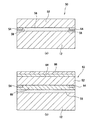
本願発明は上記の実施形態に限定されない。たとえば図4に示すように、第1ベースフィルム32の一面34に加飾層16を印刷形成し(図4(a))、第2ベースフィルム40の一面42に光学フィルム14の材料38をコーター等で積層してもよい(図4(b))。図4(a)と(b)はいずれが先であってもよいし、同時であってもよい。材料38が硬化する前に光学フィルム14の材料38の中に加飾層16が入るように、2枚のベースフィルム32、40で光学フィルム14の材料38と加飾層16を挟み込む(図4(c))。その後は上記の実施形態と同様に、材料38を硬化させ、ベースフィルム32、40を剥がすことでカバーフィルム10が完成する(図4(d))。本願において、光学フィルム14の材料38と加飾層16が上記のように第1ベースフィルム32と第2ベースフィルム40に挟まれるのであれば、図3のようにしてもよいし、図4のようにしてもよい。
The present invention is not limited to the above embodiment. For example, as shown in FIG. 4, the
光学フィルム14の材料38は、上記の紫外線硬化樹脂に限定されず、熱硬化型樹脂であってもよい。たとえば、ウレタン樹脂、アクリル樹脂、フェノール樹脂、アミノ樹脂、不飽和ポリエステル樹脂、エポキシ樹脂などの種々の樹脂が挙げられる。熱硬化型樹脂を使用すれば、光学フィルム14の材料38を硬化させるとき、加熱する。
The
その他、本発明は、その主旨を逸脱しない範囲で当業者の知識に基づき種々の改良、修正、変更を加えた態様で実施できるものである。 In addition, the present invention can be embodied in various modified, modified, and changed forms based on the knowledge of those skilled in the art without departing from the gist of the present invention.
10:カバーフィルム
12:ディスプレイ
14:光学フィルム
16:加飾層
18:光学フィルムの中央部
20:光学フィルムの外周部
22:ディスプレイの表示部分
24:ディスプレイの外周部
26:光学フィルムの一面
27:光学フィルムの他面
28:加飾層の表面
30:光学透明接着剤層
32:第1ベースフィルム
34:第1ベースフィルムの一面
38:光学フィルムの材料
40:第2ベースフィルム
42:第2ベースフィルムの一面
10: cover film 12: display 14: optical film 16: decorative layer 18:
Claims (9)
前記光学フィルムの外周部に形成され、該光学フィルムとで面一になった加飾層と、
で構成され、
ディスプレイの前面に配置されるカバーフィルム。 An optical film comprising a central portion and an outer peripheral portion, wherein the thickness of the outer peripheral portion is thinner than the thickness of the central portion,
A decorative layer formed on the outer peripheral portion of the optical film and flush with the optical film,
Consists of
Cover film placed on the front of the display.
2枚のベースフィルムを準備する工程と、
前記一のベースフィルムの一面に加飾層を形成する工程と、
前記一のベースフィルムの一面および加飾層を光学フィルムの材料で覆った状態で、2枚のベースフィルムで光学フィルムの材料と加飾層を挟み込む工程と、
前記光学フィルムの材料を硬化させて光学フィルムを形成する工程と、
前記光学フィルムと加飾層を2枚のベースフィルムから剥がす工程と、
を備えたカバーフィルムの製造方法。 A method of manufacturing a cover film disposed on a front surface of a display,
Preparing two base films;
Forming a decorative layer on one surface of the one base film;
In a state where the one surface and the decorative layer of the one base film are covered with the material of the optical film, a step of sandwiching the material of the optical film and the decorative layer with two base films,
Curing the material of the optical film to form an optical film,
Removing the optical film and the decorative layer from the two base films;
A method for producing a cover film comprising:
前記光学フィルムを形成する工程は、紫外線照射または加熱によって光学フィルムを形成する請求項6または7のカバーフィルムの製造方法。 The transparent resin is an ultraviolet curable resin or a thermosetting resin,
The method of manufacturing a cover film according to claim 6, wherein the step of forming the optical film includes forming the optical film by ultraviolet irradiation or heating.
前記カバーフィルムをディスプレイの前面に張り付ける工程と、
を備えたディスプレイの製造方法。 A step of manufacturing a cover film by the method of manufacturing a cover film according to any one of claims 6 to 8,
Attaching the cover film to the front of the display,
A method for manufacturing a display comprising:
Priority Applications (1)
| Application Number | Priority Date | Filing Date | Title |
|---|---|---|---|
| JP2018131863A JP2020008790A (en) | 2018-07-11 | 2018-07-11 | Cover film, display having the same, manufacturing method of cover film, and manufacturing method of display |
Applications Claiming Priority (1)
| Application Number | Priority Date | Filing Date | Title |
|---|---|---|---|
| JP2018131863A JP2020008790A (en) | 2018-07-11 | 2018-07-11 | Cover film, display having the same, manufacturing method of cover film, and manufacturing method of display |
Publications (1)
| Publication Number | Publication Date |
|---|---|
| JP2020008790A true JP2020008790A (en) | 2020-01-16 |
Family
ID=69151633
Family Applications (1)
| Application Number | Title | Priority Date | Filing Date |
|---|---|---|---|
| JP2018131863A Pending JP2020008790A (en) | 2018-07-11 | 2018-07-11 | Cover film, display having the same, manufacturing method of cover film, and manufacturing method of display |
Country Status (1)
| Country | Link |
|---|---|
| JP (1) | JP2020008790A (en) |
Citations (8)
| Publication number | Priority date | Publication date | Assignee | Title |
|---|---|---|---|---|
| JP2000326447A (en) * | 1999-05-21 | 2000-11-28 | Dainippon Printing Co Ltd | Hard coat film |
| WO2009131057A1 (en) * | 2008-04-21 | 2009-10-29 | 旭硝子株式会社 | Mold-releasing film |
| KR20120060962A (en) * | 2010-09-27 | 2012-06-12 | 삼성모바일디스플레이주식회사 | Display device |
| JP2013084526A (en) * | 2011-10-12 | 2013-05-09 | Asahi Glass Co Ltd | Manufacturing method of electronic device and manufacturing method of carrier substrate with resin layer |
| JP2013221985A (en) * | 2012-04-13 | 2013-10-28 | Konica Minolta Inc | Display cover member and manufacturing method of the same |
| JP2014115306A (en) * | 2011-10-20 | 2014-06-26 | Fujikura Ltd | Decorative film for display device and protection panel |
| JP2015015015A (en) * | 2013-06-05 | 2015-01-22 | 日本写真印刷株式会社 | Cover sheet for touch sensor, cover base material for touch sensor, touch sensor, and manufacturing method of cover sheet for touch sensor |
| US20150239211A1 (en) * | 2012-08-14 | 2015-08-27 | Lg Hausys, Ltd. | Laminate comprising adhesive layer and method for manufacturing same |
-
2018
- 2018-07-11 JP JP2018131863A patent/JP2020008790A/en active Pending
Patent Citations (8)
| Publication number | Priority date | Publication date | Assignee | Title |
|---|---|---|---|---|
| JP2000326447A (en) * | 1999-05-21 | 2000-11-28 | Dainippon Printing Co Ltd | Hard coat film |
| WO2009131057A1 (en) * | 2008-04-21 | 2009-10-29 | 旭硝子株式会社 | Mold-releasing film |
| KR20120060962A (en) * | 2010-09-27 | 2012-06-12 | 삼성모바일디스플레이주식회사 | Display device |
| JP2013084526A (en) * | 2011-10-12 | 2013-05-09 | Asahi Glass Co Ltd | Manufacturing method of electronic device and manufacturing method of carrier substrate with resin layer |
| JP2014115306A (en) * | 2011-10-20 | 2014-06-26 | Fujikura Ltd | Decorative film for display device and protection panel |
| JP2013221985A (en) * | 2012-04-13 | 2013-10-28 | Konica Minolta Inc | Display cover member and manufacturing method of the same |
| US20150239211A1 (en) * | 2012-08-14 | 2015-08-27 | Lg Hausys, Ltd. | Laminate comprising adhesive layer and method for manufacturing same |
| JP2015015015A (en) * | 2013-06-05 | 2015-01-22 | 日本写真印刷株式会社 | Cover sheet for touch sensor, cover base material for touch sensor, touch sensor, and manufacturing method of cover sheet for touch sensor |
Similar Documents
| Publication | Publication Date | Title |
|---|---|---|
| JP5998882B2 (en) | Transfer film and transfer film manufacturing method | |
| EP2181845B1 (en) | Decoration sheet and method of manufacturing the same | |
| US10449705B2 (en) | Transfer film for in-mold molding, method for producing in-mold molded product, and molded product | |
| KR102188336B1 (en) | Transparent laminated film for pen input device and manufacturing method thereof | |
| JP5979026B2 (en) | Transfer film for simultaneous decoration | |
| KR101481228B1 (en) | Transfer film for the exterior, method for preparing the same and in-mold injection moulded article | |
| JP6245178B2 (en) | Transfer film, method for producing molded product, and method for producing transfer film | |
| JP2010167712A (en) | Nail seal having flexibility | |
| KR20090130080A (en) | Insert Molding Film and Resin Molded Products Using the Same | |
| JP6942944B2 (en) | Concavo-convex transfer film | |
| TW202300336A (en) | Protective film, optical film, laminate, polarizing plate, image display device and method for producing said polarizing plate | |
| JP2011005766A (en) | Laminate with self-repairable layer, and molding | |
| EP3950341B1 (en) | Transfer sheet and method of manufacturing decorative molded product | |
| JP5712742B2 (en) | Optical laminate | |
| JP6287526B2 (en) | Hard coat transfer foil and molded product using the hard coat transfer foil | |
| JP5288163B2 (en) | Method for producing hologram self-adsorption label | |
| JP2020008790A (en) | Cover film, display having the same, manufacturing method of cover film, and manufacturing method of display | |
| JP5126522B2 (en) | Method for manufacturing hologram self-adhesive label, hologram self-adhesive label, and medium with hologram | |
| JP2014004155A (en) | Nail decoration sticker, and method for manufacturing the same | |
| JP2011073148A (en) | Skin material and compound molding with improved tactile feeling using the same | |
| JP2015196246A (en) | Manufacturing method of pattern printing laminate with release substrate and manufacturing method of pattern printing laminate, and pattern printing laminate with release substrate, pattern printing laminate, and intermediate laminate | |
| JP2019211592A (en) | Antireflection film and method for manufacturing the same | |
| JP4583867B2 (en) | Method for producing a three-dimensional molded product having an ultraviolet curable resin coating on the surface | |
| JP2008018579A (en) | Decorative sheet and decorative board using the same | |
| KR20240149467A (en) | Anti-wrinkle functioning laminate for flexible displays and method of manufacturing the same |
Legal Events
| Date | Code | Title | Description |
|---|---|---|---|
| A621 | Written request for application examination |
Free format text: JAPANESE INTERMEDIATE CODE: A621 Effective date: 20210322 |
|
| RD01 | Notification of change of attorney |
Free format text: JAPANESE INTERMEDIATE CODE: A7421 Effective date: 20211116 |
|
| A977 | Report on retrieval |
Free format text: JAPANESE INTERMEDIATE CODE: A971007 Effective date: 20220131 |
|
| A131 | Notification of reasons for refusal |
Free format text: JAPANESE INTERMEDIATE CODE: A131 Effective date: 20220201 |
|
| A521 | Request for written amendment filed |
Free format text: JAPANESE INTERMEDIATE CODE: A523 Effective date: 20220323 |
|
| A02 | Decision of refusal |
Free format text: JAPANESE INTERMEDIATE CODE: A02 Effective date: 20220705 |