JP2020032364A - ステージ測定治具、塗布装置およびステージ測定方法 - Google Patents
ステージ測定治具、塗布装置およびステージ測定方法 Download PDFInfo
- Publication number
- JP2020032364A JP2020032364A JP2018161310A JP2018161310A JP2020032364A JP 2020032364 A JP2020032364 A JP 2020032364A JP 2018161310 A JP2018161310 A JP 2018161310A JP 2018161310 A JP2018161310 A JP 2018161310A JP 2020032364 A JP2020032364 A JP 2020032364A
- Authority
- JP
- Japan
- Prior art keywords
- stage
- substrate
- transport
- vertical position
- measuring
- Prior art date
- Legal status (The legal status is an assumption and is not a legal conclusion. Google has not performed a legal analysis and makes no representation as to the accuracy of the status listed.)
- Granted
Links
Images






Classifications
-
- H—ELECTRICITY
- H10—SEMICONDUCTOR DEVICES; ELECTRIC SOLID-STATE DEVICES NOT OTHERWISE PROVIDED FOR
- H10P—GENERIC PROCESSES OR APPARATUS FOR THE MANUFACTURE OR TREATMENT OF DEVICES COVERED BY CLASS H10
- H10P72/00—Handling or holding of wafers, substrates or devices during manufacture or treatment thereof
- H10P72/06—Apparatus for monitoring, sorting, marking, testing or measuring
-
- H—ELECTRICITY
- H10—SEMICONDUCTOR DEVICES; ELECTRIC SOLID-STATE DEVICES NOT OTHERWISE PROVIDED FOR
- H10P—GENERIC PROCESSES OR APPARATUS FOR THE MANUFACTURE OR TREATMENT OF DEVICES COVERED BY CLASS H10
- H10P72/00—Handling or holding of wafers, substrates or devices during manufacture or treatment thereof
- H10P72/04—Apparatus for manufacture or treatment
- H10P72/0402—Apparatus for fluid treatment
- H10P72/0406—Apparatus for fluid treatment for cleaning followed by drying, rinsing, stripping, blasting or the like
-
- H—ELECTRICITY
- H10—SEMICONDUCTOR DEVICES; ELECTRIC SOLID-STATE DEVICES NOT OTHERWISE PROVIDED FOR
- H10P—GENERIC PROCESSES OR APPARATUS FOR THE MANUFACTURE OR TREATMENT OF DEVICES COVERED BY CLASS H10
- H10P72/00—Handling or holding of wafers, substrates or devices during manufacture or treatment thereof
- H10P72/04—Apparatus for manufacture or treatment
- H10P72/0448—Apparatus for applying a liquid, a resin, an ink or the like
-
- H—ELECTRICITY
- H10—SEMICONDUCTOR DEVICES; ELECTRIC SOLID-STATE DEVICES NOT OTHERWISE PROVIDED FOR
- H10P—GENERIC PROCESSES OR APPARATUS FOR THE MANUFACTURE OR TREATMENT OF DEVICES COVERED BY CLASS H10
- H10P72/00—Handling or holding of wafers, substrates or devices during manufacture or treatment thereof
- H10P72/70—Handling or holding of wafers, substrates or devices during manufacture or treatment thereof for supporting or gripping
-
- H—ELECTRICITY
- H10—SEMICONDUCTOR DEVICES; ELECTRIC SOLID-STATE DEVICES NOT OTHERWISE PROVIDED FOR
- H10P—GENERIC PROCESSES OR APPARATUS FOR THE MANUFACTURE OR TREATMENT OF DEVICES COVERED BY CLASS H10
- H10P74/00—Testing or measuring during manufacture or treatment of wafers, substrates or devices
- H10P74/23—Testing or measuring during manufacture or treatment of wafers, substrates or devices characterised by multiple measurements, corrections, marking or sorting processes
Landscapes
- Coating Apparatus (AREA)
- Application Of Or Painting With Fluid Materials (AREA)
- Exposure Of Semiconductors, Excluding Electron Or Ion Beam Exposure (AREA)
Abstract
Description
図1は、実施形態の基板処理装置の一例である塗布装置1の全体構成を模式的に示す側面図である。図2は、実施形態の塗布装置1を鉛直方向上側から見た概略平面図である。図3は、実施形態の塗布機構6を除いた塗布装置1を示す概略平面図である。図4は、図2に示すA−A線に沿う位置における塗布装置1の概略断面図である。図5は、実施形態の浮上ステージ3の一部を示す概略平面図である。
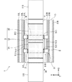
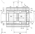
図6は、実施形態のステージ測定治具8を示す概略平面図である。図7は、実施形態のステージ測定治具8を示す概略正面図である。図8は、実施形態のステージ測定治具8を示す概略平面図である。ステージ測定治具8は、浮上ステージ3(ステージ31−33)の各上面31S−33Sの鉛直位置を測定する装置である。ここでは、ステージ測定治具8は、各上面31S−33Sの平面出しをすることを目的に使用される。
図10は、浮上ステージ3の各上面31S−33Sの鉛直位置を測定および調整する処理フローを示す図である。以下に説明する処理フローは、一例であり、これに限定されるものではない。
ステージ測定治具8によると、塗布装置1において基板Wを搬送するために設けられた搬送シャトル5に各ステージ測定器81を接続して、ステージ測定器81を搬送方向D1に移動させる。このため、浮上ステージ3の搬送方向D1における鉛直位置の分布を効率良く測定できる。したがって、浮上ステージ3の各上面31S−33Sの傾きを効率良く測定できる。
以上、実施形態について説明してきたが、本発明は上記のようなものに限定されるものではなく、様々な変形が可能である。
13 調整機構
131 レベリングボルト
133 支持板
3 浮上ステージ
31 入口浮上ステージ
32 塗布ステージ
321h 噴出口
322h 吸引口
33 出口浮上ステージ
31S,32S,33S 上面
31h,33h 噴出口
35 浮上制御機構
5 搬送シャトル
6 塗布機構
8 ステージ測定治具
81 ステージ測定器
83 架橋構造
831 梁部
831S 側面
832,833 支柱部
841,843 連結具
D1 搬送方向
D2 搬送幅方向
W 基板
Claims (7)
- 搬送シャトルによって既定の搬送方向に搬送される基板に浮上力を付与する浮上ステージが有する平面であって、かつ、エアを噴出する複数の孔が形成された鉛直方向上向きである上面の鉛直位置を測定するステージ測定治具であって、
前記浮上ステージの前記上面の鉛直位置を測定する少なくとも1つのステージ測定器と、
前記ステージ測定器を前記搬送方向に移動可能となるように前記搬送シャトルに接続する接続部と、
を含む、ステージ測定治具。 - 請求項1のステージ測定治具であって、
前記接続部は、
前記搬送方向に直交する搬送幅方向に延びており、前記ステージ測定器を前記上面の上方にて支持する梁部と、
前記梁部を前記搬送シャトルに対して取り外し可能に連結する連結具と、
を備える、ステージ測定治具。 - 請求項1又は請求項2のステージ測定治具であって、
前記上面の一部である対象部分の鉛直位置が浮上ステージに設けられた調整機構によって調整可能であり、
前記ステージ測定器は、前記対象部分の鉛直位置を測定可能な位置に設けられている、ステージ測定治具。 - 請求項1から請求項3のいずれか1項のステージ測定治具であって、
前記搬送方向に直交する搬送幅方向に間隔をあけて、複数の前記ステージ測定器が設けられている、ステージ測定治具。 - 基板に処理液を塗布する塗布装置であって、
基板を既定の方向に搬送する搬送シャトルと、
鉛直上向きの上面に設けられた複数の孔からエアを噴出することによって、前記搬送シャトルが搬送方向に搬送する基板に浮上力を付与する浮上ステージと、
前記エアを供給するエア供給部と、
前記上面の鉛直位置を測定する少なくとも1つのステージ測定器と、
前記ステージ測定器を前記搬送方向に移動可能となるように前記搬送シャトルに接続する接続部と、
前記上面の一部である対象部分の鉛直位置を調整する調整具と、
前記搬送シャトルによって前記搬送方向に搬送される基板に向けて処理液を吐出するノズルと、
を備える、塗布装置。 - 搬送シャトルによって既定の搬送方向に搬送される基板に浮上力を付与する浮上ステージが有する平面であって、かつ、エアを噴出する複数の孔が形成された鉛直方向上向きである上面の鉛直位置を測定するステージ測定方法であって、
(a) 接続部を介してステージ測定器を前記搬送シャトルに接続する工程と、
(b) 前記ステージ測定器を前記搬送シャトルの動力によって前記搬送方向に移動させる工程と、
(c) 前記工程(b)において、前記搬送方向に移動する前記ステージ測定器によって、前記上面における前記搬送方向に異なる部分の鉛直位置を測定する工程と、
を含む、ステージ測定方法。 - 既定の搬送方向に搬送される基板に浮上力を付与する浮上ステージが有する平面であって、かつ、エアを噴出する複数の孔が形成された鉛直方向上向きである上面の鉛直位置を測定するステージ測定治具であって、
前記浮上ステージの前記上面の鉛直位置を測定する少なくとも1つのステージ測定器と、
前記ステージ測定器を前記搬送方向に移動させる移動部と、
を含む、ステージ測定治具。
Priority Applications (3)
| Application Number | Priority Date | Filing Date | Title |
|---|---|---|---|
| JP2018161310A JP6817986B2 (ja) | 2018-08-30 | 2018-08-30 | ステージ測定治具、塗布装置およびステージ測定方法 |
| KR1020190097743A KR102308585B1 (ko) | 2018-08-30 | 2019-08-09 | 스테이지 측정 지그, 도포 장치 및 스테이지 측정 방법 |
| CN201921443391.9U CN210837662U (zh) | 2018-08-30 | 2019-08-30 | 载物台测定夹具及涂敷装置 |
Applications Claiming Priority (1)
| Application Number | Priority Date | Filing Date | Title |
|---|---|---|---|
| JP2018161310A JP6817986B2 (ja) | 2018-08-30 | 2018-08-30 | ステージ測定治具、塗布装置およびステージ測定方法 |
Publications (2)
| Publication Number | Publication Date |
|---|---|
| JP2020032364A true JP2020032364A (ja) | 2020-03-05 |
| JP6817986B2 JP6817986B2 (ja) | 2021-01-20 |
Family
ID=69666510
Family Applications (1)
| Application Number | Title | Priority Date | Filing Date |
|---|---|---|---|
| JP2018161310A Active JP6817986B2 (ja) | 2018-08-30 | 2018-08-30 | ステージ測定治具、塗布装置およびステージ測定方法 |
Country Status (3)
| Country | Link |
|---|---|
| JP (1) | JP6817986B2 (ja) |
| KR (1) | KR102308585B1 (ja) |
| CN (1) | CN210837662U (ja) |
Cited By (3)
| Publication number | Priority date | Publication date | Assignee | Title |
|---|---|---|---|---|
| KR102123334B1 (ko) * | 2020-03-16 | 2020-06-16 | 홍유길 | 태양광 모듈용 유체처리수단 |
| KR102134588B1 (ko) * | 2020-03-11 | 2020-07-16 | 홍유길 | 지주 베이스 내장형 태양광 모듈 구조물 시공방법 |
| JP2025176882A (ja) * | 2024-05-22 | 2025-12-05 | 株式会社Screenホールディングス | 塗布装置 |
Citations (8)
| Publication number | Priority date | Publication date | Assignee | Title |
|---|---|---|---|---|
| JP2005028202A (ja) * | 2003-07-07 | 2005-02-03 | Hitachi Industries Co Ltd | テーブル平行度調整装置とそれを用いたディスペンサ |
| JP2005218948A (ja) * | 2004-02-05 | 2005-08-18 | Dainippon Printing Co Ltd | 処理装置および処理方法 |
| JP2008132422A (ja) * | 2006-11-28 | 2008-06-12 | Tokyo Electron Ltd | 塗布方法及び塗布装置 |
| JP2010251535A (ja) * | 2009-04-16 | 2010-11-04 | Toray Eng Co Ltd | 基板処理装置 |
| JP2012134419A (ja) * | 2010-12-24 | 2012-07-12 | Tokyo Ohka Kogyo Co Ltd | 塗布装置及び塗布方法 |
| JP2013131770A (ja) * | 2013-02-04 | 2013-07-04 | Tokyo Ohka Kogyo Co Ltd | 塗布装置 |
| JP2013191604A (ja) * | 2012-03-12 | 2013-09-26 | Toray Eng Co Ltd | 塗布装置 |
| US20160014906A1 (en) * | 2014-07-11 | 2016-01-14 | Voltera Inc. | Apparatus and method for printing circuitry |
Family Cites Families (2)
| Publication number | Priority date | Publication date | Assignee | Title |
|---|---|---|---|---|
| JP5486030B2 (ja) | 2012-02-15 | 2014-05-07 | 東京エレクトロン株式会社 | 塗布装置 |
| JP2013171770A (ja) | 2012-02-22 | 2013-09-02 | Seiko Epson Corp | 加熱用トレイおよび加熱装置 |
-
2018
- 2018-08-30 JP JP2018161310A patent/JP6817986B2/ja active Active
-
2019
- 2019-08-09 KR KR1020190097743A patent/KR102308585B1/ko active Active
- 2019-08-30 CN CN201921443391.9U patent/CN210837662U/zh active Active
Patent Citations (8)
| Publication number | Priority date | Publication date | Assignee | Title |
|---|---|---|---|---|
| JP2005028202A (ja) * | 2003-07-07 | 2005-02-03 | Hitachi Industries Co Ltd | テーブル平行度調整装置とそれを用いたディスペンサ |
| JP2005218948A (ja) * | 2004-02-05 | 2005-08-18 | Dainippon Printing Co Ltd | 処理装置および処理方法 |
| JP2008132422A (ja) * | 2006-11-28 | 2008-06-12 | Tokyo Electron Ltd | 塗布方法及び塗布装置 |
| JP2010251535A (ja) * | 2009-04-16 | 2010-11-04 | Toray Eng Co Ltd | 基板処理装置 |
| JP2012134419A (ja) * | 2010-12-24 | 2012-07-12 | Tokyo Ohka Kogyo Co Ltd | 塗布装置及び塗布方法 |
| JP2013191604A (ja) * | 2012-03-12 | 2013-09-26 | Toray Eng Co Ltd | 塗布装置 |
| JP2013131770A (ja) * | 2013-02-04 | 2013-07-04 | Tokyo Ohka Kogyo Co Ltd | 塗布装置 |
| US20160014906A1 (en) * | 2014-07-11 | 2016-01-14 | Voltera Inc. | Apparatus and method for printing circuitry |
Cited By (3)
| Publication number | Priority date | Publication date | Assignee | Title |
|---|---|---|---|---|
| KR102134588B1 (ko) * | 2020-03-11 | 2020-07-16 | 홍유길 | 지주 베이스 내장형 태양광 모듈 구조물 시공방법 |
| KR102123334B1 (ko) * | 2020-03-16 | 2020-06-16 | 홍유길 | 태양광 모듈용 유체처리수단 |
| JP2025176882A (ja) * | 2024-05-22 | 2025-12-05 | 株式会社Screenホールディングス | 塗布装置 |
Also Published As
| Publication number | Publication date |
|---|---|
| KR102308585B1 (ko) | 2021-10-01 |
| KR20200026051A (ko) | 2020-03-10 |
| JP6817986B2 (ja) | 2021-01-20 |
| CN210837662U (zh) | 2020-06-23 |
Similar Documents
| Publication | Publication Date | Title |
|---|---|---|
| CN101441337B (zh) | 传送和约束大型扁平柔性介质的高精度气浮轴承分轴台 | |
| KR101299816B1 (ko) | 도포 방법 및 도포 장치 | |
| JP4652351B2 (ja) | 基板支持装置、基板支持方法 | |
| CN210837662U (zh) | 载物台测定夹具及涂敷装置 | |
| JP2009061395A (ja) | 塗布装置及び塗布方法 | |
| CN110676192B (zh) | 基板处理装置和基板处理方法 | |
| JP5265099B2 (ja) | 基板検査装置 | |
| JP5349770B2 (ja) | 塗布装置及び塗布方法 | |
| JP4226500B2 (ja) | 基板搬送機構および塗布膜形成装置 | |
| JP6738373B2 (ja) | 基板処理装置および基板処理方法 | |
| JP5386217B2 (ja) | 表示パネル搬送装置および表示パネルモジュール組立装置 | |
| JP6890438B2 (ja) | 浮上量算出装置、塗布装置および塗布方法 | |
| JP7470749B2 (ja) | 塗布装置 | |
| CN121004100A (zh) | 涂布装置 |
Legal Events
| Date | Code | Title | Description |
|---|---|---|---|
| A621 | Written request for application examination |
Free format text: JAPANESE INTERMEDIATE CODE: A621 Effective date: 20190401 |
|
| A977 | Report on retrieval |
Free format text: JAPANESE INTERMEDIATE CODE: A971007 Effective date: 20200729 |
|
| A131 | Notification of reasons for refusal |
Free format text: JAPANESE INTERMEDIATE CODE: A131 Effective date: 20200811 |
|
| A521 | Request for written amendment filed |
Free format text: JAPANESE INTERMEDIATE CODE: A523 Effective date: 20201005 |
|
| TRDD | Decision of grant or rejection written | ||
| A01 | Written decision to grant a patent or to grant a registration (utility model) |
Free format text: JAPANESE INTERMEDIATE CODE: A01 Effective date: 20201208 |
|
| A61 | First payment of annual fees (during grant procedure) |
Free format text: JAPANESE INTERMEDIATE CODE: A61 Effective date: 20201225 |
|
| R150 | Certificate of patent or registration of utility model |
Ref document number: 6817986 Country of ref document: JP Free format text: JAPANESE INTERMEDIATE CODE: R150 |
|
| R250 | Receipt of annual fees |
Free format text: JAPANESE INTERMEDIATE CODE: R250 |
|
| R250 | Receipt of annual fees |
Free format text: JAPANESE INTERMEDIATE CODE: R250 |
|
| R250 | Receipt of annual fees |
Free format text: JAPANESE INTERMEDIATE CODE: R250 |