JP2020091402A - Light source device for exposure - Google Patents
Light source device for exposure Download PDFInfo
- Publication number
- JP2020091402A JP2020091402A JP2018228553A JP2018228553A JP2020091402A JP 2020091402 A JP2020091402 A JP 2020091402A JP 2018228553 A JP2018228553 A JP 2018228553A JP 2018228553 A JP2018228553 A JP 2018228553A JP 2020091402 A JP2020091402 A JP 2020091402A
- Authority
- JP
- Japan
- Prior art keywords
- light
- optical system
- semiconductor laser
- light source
- source device
- Prior art date
- Legal status (The legal status is an assumption and is not a legal conclusion. Google has not performed a legal analysis and makes no representation as to the accuracy of the status listed.)
- Pending
Links
Images




Classifications
-
- G—PHYSICS
- G03—PHOTOGRAPHY; CINEMATOGRAPHY; ANALOGOUS TECHNIQUES USING WAVES OTHER THAN OPTICAL WAVES; ELECTROGRAPHY; HOLOGRAPHY
- G03F—PHOTOMECHANICAL PRODUCTION OF TEXTURED OR PATTERNED SURFACES, e.g. FOR PRINTING, FOR PROCESSING OF SEMICONDUCTOR DEVICES; MATERIALS THEREFOR; ORIGINALS THEREFOR; APPARATUS SPECIALLY ADAPTED THEREFOR
- G03F7/00—Photomechanical, e.g. photolithographic, production of textured or patterned surfaces, e.g. printing surfaces; Materials therefor, e.g. comprising photoresists; Apparatus specially adapted therefor
- G03F7/20—Exposure; Apparatus therefor
-
- H—ELECTRICITY
- H05—ELECTRIC TECHNIQUES NOT OTHERWISE PROVIDED FOR
- H05K—PRINTED CIRCUITS; CASINGS OR CONSTRUCTIONAL DETAILS OF ELECTRIC APPARATUS; MANUFACTURE OF ASSEMBLAGES OF ELECTRICAL COMPONENTS
- H05K3/00—Apparatus or processes for manufacturing printed circuits
Landscapes
- Engineering & Computer Science (AREA)
- Physics & Mathematics (AREA)
- General Physics & Mathematics (AREA)
- Manufacturing & Machinery (AREA)
- Microelectronics & Electronic Packaging (AREA)
- Exposure And Positioning Against Photoresist Photosensitive Materials (AREA)
Abstract
【課題】複数の半導体レーザ光源を用いて、放電ランプを用いた光源装置と同等の角度分布の光を供給する露光用光源装置を提供する。【解決手段】複数の半導体レーザ光源と、半導体レーザ光源から出射された光線束を、略平行の光線束に変換して出射する、複数のコリメート光学系と、コリメート光学系から出射された光線束22を集光する集光光学系12と、円形状の入射面を含む光導波路とを備え、集光光学系の入射面20における、複数の半導体レーザ光源から出射されたそれぞれの光線束22は、仮想的に集光光学系の光軸15を中心に回転させて、同一の径方向に向かって並べたときに、隣接する光線束の一部が重なり、複数の半導体レーザ光源は、集光光学系の入射面において、集光光学系の光軸からの距離が同一である光線束群に属する光線束の数が、光軸からの距離がn番目に近い第n光線束群を基準として、光軸から離れるにつれて逓減するように配置される。【選択図】図3BPROBLEM TO BE SOLVED: To provide an exposure light source device which supplies light having an angle distribution equivalent to that of a light source device using a discharge lamp by using a plurality of semiconductor laser light sources. SOLUTION: A plurality of collimating optical systems that convert a plurality of semiconductor laser light sources and light bundles emitted from the semiconductor laser light sources into substantially parallel light bundles and emit the light bundles, and a light flux emitted from the collimating optical system. A condensing optical system 12 for condensing 22 and an optical waveguide including a circular incident surface are provided, and each light bundle 22 emitted from a plurality of semiconductor laser light sources on the incident surface 20 of the condensing optical system When the optical axes 15 of the condensing optical system are virtually rotated and arranged in the same radial direction, some of the adjacent light fluxes overlap, and the plurality of semiconductor laser light sources condense. On the incident surface of the optical system, the number of light fluxes belonging to the light flux group having the same distance from the optical axis of the condensing optical system is based on the nth light bundle group whose distance from the optical axis is the nth closest. , Arranged so as to gradually decrease as the distance from the optical axis increases. [Selection diagram] FIG. 3B
Description
本発明は、露光用光源装置に関し、特に半導体レーザ光源から出射された光を用いた露光用光源装置に関する。 The present invention relates to an exposure light source device, and more particularly to an exposure light source device that uses light emitted from a semiconductor laser light source.
従来、プリント基板等の製造工程等に用いられる露光装置には光強度の高い放電ランプが用いられていた。近年では、固体光源技術の進歩に伴い、放電ランプから高効率で長寿命な半導体レーザ光源に置き換える検討が進められている。 Conventionally, a discharge lamp having a high light intensity has been used for an exposure device used in a manufacturing process of a printed circuit board or the like. In recent years, with the progress of solid-state light source technology, studies are being made to replace a discharge lamp with a highly efficient and long-life semiconductor laser light source.
単体の半導体レーザ光源では、露光装置の光源としては放射光束が少ない。高い強度の光を得るためには、複数の半導体レーザ光源を配置し、それぞれの半導体レーザ光源から出射された光を集光する方法が考えられる。例えば、特許文献1には、複数の半導体レーザ光源と、それぞれの半導体レーザ光源に対応する光ファイバを備えた、フレキシブルプリント基板用の露光装置が開示されている。
With a single semiconductor laser light source, the emitted light flux is small as a light source of the exposure apparatus. In order to obtain high intensity light, a method of arranging a plurality of semiconductor laser light sources and condensing the light emitted from each semiconductor laser light source can be considered. For example,
複数の半導体レーザ光源から出射される光を集光するには、コリメートレンズや集光レンズを用いて集光する方法が考えられる。しかし、本発明者らは、露光装置用の光源装置を、放電ランプを用いた光源装置から、複数の半導体レーザ光源より出射された光を、光学系によって集光する光源装置へと置き換えることを検討したところ、以下のような課題が存在することを突き止めた。以下、図面を参照しながら説明する。 To collect light emitted from a plurality of semiconductor laser light sources, a method of collecting light using a collimator lens or a condenser lens can be considered. However, the present inventors replace the light source device for the exposure apparatus with a light source device that condenses light emitted from a plurality of semiconductor laser light sources by an optical system from a light source device that uses a discharge lamp. Upon examination, they found that the following problems existed. Hereinafter, description will be given with reference to the drawings.
図7Aは、半導体レーザ光源100とコリメートレンズ101(「コリメーションレンズ」とも称される。)と集光レンズ102及びロッドインテグレータ104で構成された、露光用光源装置を模式的に示した図面である。図7Aは、複数の半導体レーザ光源100から出射される光(レーザ光)の各主光線及び各光線束の進行経路を模式的に図示している。なお、本明細書では、半導体レーザ光源100の中心から光軸140と平行に出射される光線を「主光線」と称し、半導体レーザ光源100から出射される束状に形成された光線群を「光線束」と称する。
FIG. 7A is a drawing schematically showing an exposure light source device including a semiconductor
図7Aにおいては、ロッドインテグレータ104の入射面105に対して直交する軸を光軸140とする。また、光軸140方向をZ方向とし、Z方向に直交する平面をXY平面とし、入射面105に対する光の入射角をθ1とする。
In FIG. 7A, an axis orthogonal to the
半導体レーザ光源100から出射された光線束(121a,121b,121c)は、コリメートレンズ101によって略平行な光線束(122a,122b,122c)に変換される。光線束(122a,122b,122c)は互いに平行であって、相互に重なり合うことはなく、後段の集光レンズ102に入射する。集光レンズ102に入射した光線束(122a,122b,122c)は、集光レンズ102の焦点位置150に向かって集光する光線束(123a,123b,123c)に変換される。
The light flux (121a, 121b, 121c) emitted from the semiconductor
集光レンズ102の後段には、集光レンズ102によって集光された光線束(123a,123b,123c)の光強度分布を均一化するため、ロッドインテグレータ104が配置される。ロッドインテグレータ104は、入射面105が、集光レンズ102の焦点位置150と合うように配置される。
A
ここで、半導体レーザ光源100及びコリメートレンズ101を完全に密接して配置できないため、各光線束(122a,122b,122c)の間に隙間が生じ、集光レンズ102の入射面103において、光が存在する場所としない場所が生じてしまい、照度ムラが発生してしまう。
Here, since the semiconductor
従って、集光レンズ102の出射面に発生した照度ムラが発生した光を、集光レンズ102によって焦点位置150に集光するように変換された光線束(123a,123b,123c)は、一部の角度範囲において光が存在しない、又は主光線(110a,110b,110c)近傍と比較して、極めて光強度の低い領域130が生じてしまう。
Therefore, a part of the light flux (123a, 123b, 123c) converted by the
さらに、集光レンズ102の入射面103をXY平面で見た場合を説明する。図7Bは、図7Aの集光レンズ102を入射面103側からZ方向に向かって見たときの模式的な図面である。なお、説明の便宜のため、Y方向においても、X方向と同じ間隔で、同数の半導体レーザ光源100及びコリメートレンズ101が整列されており、光線束122bの主光線110bが、光軸140と一致しているものとした。また、XY平面上の相対的な位置関係の理解を容易にするため、図7Aには、集光レンズ102の入射面103に入射される光線束(122a,122b,122c)に加えて、集光レンズ102から+Z方向に位置するロッドインテグレータ104についても図示されている。
Further, a case where the
各光線束(122a,122b,122c)は、集光レンズ102の入射面103において楕円形状である。図8は、半導体レーザチップ200の構造を模式的に示す斜視図である。図8に示すような、いわゆる「端面発光型」の半導体レーザチップ200の場合、エミッタ201から出射される光線束121は、楕円錐型を示すことが知られている。従って、図7Bに示すように、各光線束(122a,122b,122c)の断面は楕円形状となる。なお、図7Aに示す半導体レーザ光源100は、図8に示す半導体レーザチップ200をケーシングしたレーザ光源である。半導体レーザ光源100は、光の出射窓の中心を主光線(110a,110b,110c)が通過するように、光を出射するレーザ光源である。
Each ray bundle (122a, 122b, 122c) has an elliptical shape on the
本明細書では、光軸(図8に示すZ方向)に直交する2方向(X方向及びY方向)のうち、光線束121の発散角が大きい方向(図8に示すY方向)を、「Fast軸方向」と呼び、光線束121の発散角が小さい方向(図8に示すX方向)を、「Slow軸方向」と呼ぶ。ここで、発散角とは、光強度が最大となる主光線(110a,110b,110c)の1/e2の光強度で進行する光線と、主光線(110a,110b,110c)とがなす角の2倍の角を指す。
In the present specification, of the two directions (X direction and Y direction) orthogonal to the optical axis (Z direction shown in FIG. 8), the direction in which the divergence angle of the
図7Bに示すように、集光レンズ102の入射面103では、各光線束(122a,122b,122c)は、光軸140を中心とした同心円上において、光が存在しない、又は主光線近傍と比較して、極めて光強度の低い領域130が生じる。これは、上述の理由と同様で、半導体レーザ光源100及びコリメートレンズ101を完全に密接して配置できないためである。
As shown in FIG. 7B, on the
ロッドインテグレータ104は、入射された光を側面で繰り返し全反射させながら、出射面106(図7A参照)へと導くものであるため、XY平面上の位置における光強度分布(以下、「位置分布)という。)の均一性を向上させる効果はあるが、ロッドインテグレータ104の入射面105における入射角θ1ごとの光強度分布(以下、「角度分布」という。)は出射面106においても保持されるため、角度分布の均一性を向上させる効果はない。
Since the
従って、ロッドインテグレータ104を用いても、一部の角度範囲において光が存在しない、又は主光線近傍と比較して、極めて光強度の低い領域は解消されない。つまり、集光レンズ102の出射面に発生した角度分布のムラは、ロッドインテグレータ104の出射面106から出射される光においても解消されない。
Therefore, even if the
ここで、放電ランプ160を用いた光源装置から出射される光の角度分布について説明する。図9は、放電ランプ160を用いた光源装置の構成例を模式的に示す図面である。図9に示すように、放電ランプ160を用いた光源装置は、管体161内に放電ガスを封入し、陰極162と陽極163の間で放電されることで発光部164から光が出射される。
Here, the angular distribution of the light emitted from the light source device using the
放電ランプ160から出射された光のうち、一部の光は、楕円ミラー165によって反射されて、ロッドインテグレータ104の入射面105に集光される。楕円ミラー165は、発光部164と、ロットインテグレータ104の入射面105の2か所を焦点とする、楕円弧の形状をなしている。
A part of the light emitted from the
図9に示すように、ロッドインテグレータ104の入射面105における、最も大きな光の入射角が角度α1となるように構成されている。また、発光部164から出射される光のうち、光軸15の近傍を進行する光は、管体161の一部によって遮られてしまい、ロッドインテグレータ104の入射面105には到達しない。そのため、入射角が角度α2よりも小さい領域には光が存在しない。
As shown in FIG. 9, the maximum incident angle of light on the
つまり、図9に示すような、放電ランプ160を用いた光源装置の角度分布は、光軸140から、角度α2より小さい角度範囲には、光が存在せず、角度α2から角度α1の範囲に光が連続的に分布している。また、放電ランプ160から全方向に一様に出射された光のうち、楕円ミラー165で反射された一部の光は、ロッドインテグレータ104の入射面105における入射角が小さいほど、光線同士が密となり、光強度が高くなる。
That is, as shown in FIG. 9, the angle distribution of the light source device using the
図10は、放電ランプ160を用いた光源装置から出射される光の角度分布を模式的に示すグラフである。図10に示すように、放電ランプ160を用いた光源装置の角度分布は、入射角が0°に近い部分では、光が存在せず、集光される光が存在する角度範囲のうち、角度が小さい範囲においてピークを持ち、そこから角度が大きくなるにつれて、光強度は連続的に減少する。なお、位置分布に関しては、ロットインテグレータ104によって均一化される。
FIG. 10 is a graph schematically showing the angular distribution of the light emitted from the light source device using the
露光装置用の光源装置を、放電ランプ160を用いた光源装置から半導体レーザ光源を用いた光源装置に置き換えるため、半導体レーザ光源を用いた光源装置が、放電ランプ160を用いた光源装置と同等の光、すなわち放電ランプ160を用いた光源装置と同じ位置分布及び角度分布であることが期待されている。
Since the light source device for the exposure apparatus is replaced with the light source device using the semiconductor laser light source from the light source device using the
しかし、上述のとおり、複数の半導体レーザ光源100から出射された光を、コリメートレンズ101、集光レンズ102、及び、ロッドインテグレータ104による構成だけで、放電ランプ160を用いた場合と同等の光にはできない。すなわち、放電ランプ160を用いた光源装置の位置分布とは同等にすることができるが、角度分布は同等とならないことがわかった。
However, as described above, the light emitted from the plurality of semiconductor
本発明は、上記の課題に鑑み、複数の半導体レーザ光源を用いて、放電ランプを用いた光源装置と同等の角度分布の光を供給する露光用光源装置を提供することを目的とする。 In view of the above problems, it is an object of the present invention to provide an exposure light source device that uses a plurality of semiconductor laser light sources to supply light having an angular distribution equivalent to that of a light source device that uses a discharge lamp.
本発明に係る露光用光源装置は、
複数の半導体レーザ光源と、
前記複数の半導体レーザ光源に対応して配置され、前記半導体レーザ光源から出射された光線束を、略平行の光線束に変換して出射する、複数のコリメート光学系と、
前記コリメート光学系から出射された光線束が入射される入射面を含み、前記コリメート光学系から出射された光線束を集光する集光光学系と、
前記集光光学系から出射された光線束が集光する位置に配置された、円形状の入射面を含む光導波路とを備え、
前記集光光学系の入射面における、前記複数の半導体レーザ光源から出射されたそれぞれの光線束は、仮想的に前記集光光学系の光軸を中心に回転させて、同一の径方向に向かって並べたときに、隣接する光線束の一部が重なっており、
前記複数の半導体レーザ光源は、前記集光光学系の入射面において、前記集光光学系の光軸からの距離が同一である光線束群に属する光線束の数が、光軸からの距離がn番目に近い第n光線束群を基準として、光軸から離れるにつれて逓減するように配置されていることを特徴とする。
The exposure light source device according to the present invention is
A plurality of semiconductor laser light sources,
A plurality of collimating optical systems, which are arranged corresponding to the plurality of semiconductor laser light sources, convert the light flux emitted from the semiconductor laser light source into a substantially parallel light flux, and emit the light.
A condensing optical system that includes an incident surface on which the light flux emitted from the collimating optical system is incident, and that condenses the light flux emitted from the collimating optical system,
An optical waveguide including a circular incident surface, which is arranged at a position where a bundle of rays emitted from the condensing optical system is condensed,
The respective light fluxes emitted from the plurality of semiconductor laser light sources on the entrance surface of the condensing optical system are virtually rotated about the optical axis of the condensing optical system and are directed in the same radial direction. When arranged side by side, some of the adjacent ray bundles overlap,
In the plurality of semiconductor laser light sources, on the incident surface of the condensing optical system, the number of ray bundles belonging to the bundle of ray bundles having the same distance from the optical axis of the condensing optical system is the distance from the optical axis. It is characterized in that it is arranged so as to gradually decrease with increasing distance from the optical axis, with the n-th ray bundle group close to the n-th reference.
上記露光用光源装置は、集光光学系の入射面において、各半導体レーザ光源から出射されたそれぞれの光線束は、集光光学系の光軸を中心に回転させて、同一の径方向に向かって並べたときに、隣接する光線束の一部が重なっている。なお、集光光学系の光軸を中心に回転させて、同一の径方向に向かって並べるという過程は、図3Bの説明において後述する。 In the exposure light source device, on the incident surface of the condensing optical system, the respective light fluxes emitted from the respective semiconductor laser light sources are rotated about the optical axis of the condensing optical system and directed in the same radial direction. When they are arranged side by side, some of the adjacent ray bundles overlap. The process of rotating the condensing optical system about the optical axis and arranging them in the same radial direction will be described later in the description of FIG. 3B.
上記構成によれば、図7Bに示すような、集光光学系の光軸を中心とする同心円上において、隣接する光線束群同士の間で、光が存在しない、又は主光線近傍と比較して、極めて光強度の低い領域は生じない。つまり、光軸に対する角度方向において、光が存在する領域内の一部に光が存在しない範囲がなくなる。詳細は、図3Bの説明において後述する。 According to the above configuration, as shown in FIG. 7B, on a concentric circle centered on the optical axis of the condensing optical system, light does not exist between adjacent ray bundle groups, or compared with the vicinity of the chief ray. Therefore, a region having extremely low light intensity does not occur. That is, in the angle direction with respect to the optical axis, there is no range where light does not exist in a part of the region where light exists. Details will be described later in the description of FIG. 3B.
nは任意の自然数である。また、光軸からの距離がn番目に近い第n光線束群を基準として、光軸から離れるにつれて逓減するとは、任意に定められる値nから、nの数が増えるごとに、光線束群に属する光線束の数が、断続的又は連続的に減少することを意味する。つまり、第n光線束群の次に光軸に近い光線束群に属する光線束の数は、第n光線束群に属する光線束の数と同じ又は、第n光線束群に属する光線束の数よりも少なくなるように、前記複数の半導体レーザ光源が配置されていることを意味している。 n is an arbitrary natural number. Further, with the n-th ray bundle group whose distance from the optical axis is closest to the nth as a reference, it means that the ray bundle group gradually decreases as the number of n increases from the arbitrarily determined value n. It means that the number of belonging ray bundles decreases intermittently or continuously. That is, the number of ray bundles belonging to the ray bundle group next to the optical axis next to the n-th ray bundle group is the same as the number of ray bundles belonging to the n-th ray bundle group, or of the ray bundles belonging to the n-th ray bundle group. This means that the plurality of semiconductor laser light sources are arranged so as to be less than the number.
集光光学系の光軸からの距離が同一である光線束群に属する光線束の数が多くなるほど、光導波路の入射面における入射角ごとの光強度が高くなる。つまり、上記構成によれば、光導波路の入射面における所定の入射角よりも角度が大きい範囲において、入射角が大きくなるにつれて光強度が逓減する角度分布となり、放電ランプを用いた光源装置から出射される光の角度分布に近い角度分布を示す光が得られる。 The larger the number of light bundles belonging to the light bundle group having the same distance from the optical axis of the condensing optical system, the higher the light intensity for each incident angle on the incident surface of the optical waveguide. That is, according to the above configuration, in the range where the angle of incidence on the incident surface of the optical waveguide is larger than the predetermined angle of incidence, the light intensity gradually decreases as the angle of incidence increases, and the light is emitted from the light source device using the discharge lamp. Light having an angular distribution close to that of the generated light is obtained.
なお、光軸からの距離が同一であるとは、光軸からの距離が一致しているものだけには限られず、距離の誤差が1mm以下であれば、同一の光線束群に属する光線束とみなしてもよい。 The same distance from the optical axis is not limited to the same distance from the optical axis. If the distance error is 1 mm or less, the light bundles belonging to the same light bundle group are included. May be regarded as
上記露光用光源装置は、入射面が円形状である光導波路を備える。入射面が円形状であることによって、光導波路から出射される光は、入射面における入射角を維持したまま、光軸を中心とした同心円上において均一な光に変換される。詳細は、図1Bの説明において後述する。 The exposure light source device includes an optical waveguide whose incident surface is circular. Since the incident surface is circular, the light emitted from the optical waveguide is converted into uniform light on a concentric circle centered on the optical axis while maintaining the incident angle on the incident surface. Details will be described later in the description of FIG. 1B.
上記露光用光源装置において、
複数の前記半導体レーザ光源は、同一平面上に配置されていても構わない。
In the exposure light source device,
The plurality of semiconductor laser light sources may be arranged on the same plane.
上記構成によれば、全ての半導体レーザ光源が、同一の基板上に配置されるため、各半導体レーザ光源を同一基板上で配線することができる。さらには、半導体レーザ光源が、同一基板上の冷却機構で冷却する構成とすることができる。 According to the above configuration, since all the semiconductor laser light sources are arranged on the same substrate, it is possible to wire each semiconductor laser light source on the same substrate. Furthermore, the semiconductor laser light source may be cooled by a cooling mechanism on the same substrate.
上記露光用光源装置において、
前記複数の半導体レーザ光源は、前記集光光学系の入射面において、前記集光光学系の光軸からの距離が同一である光線束群に属する光線束の数が、光軸からの距離が最も近い第1光線束群を基準として、光軸から離れるにつれて逓減するように配置されていても構わない。
In the exposure light source device,
In the plurality of semiconductor laser light sources, on the incident surface of the condensing optical system, the number of ray bundles belonging to the bundle of ray bundles having the same distance from the optical axis of the condensing optical system is the distance from the optical axis. The closest first ray bundle group may be used as a reference, and the first ray bundle group may be arranged so as to gradually decrease with distance from the optical axis.
上記構成によれば、前記第1光線束群に属する光線束の数は少なくとも2以上となる。これは、第1光線束群に属する光線束が1つでは、全ての光線束群に属する光線束の数が1となってしまい、逓減することがないためである。そうすると、前記集光光学系の光軸上には光線束が配置されることはなく、光導波路の入射面における入射角が0°付近には光が存在しない。さらに、前記第1光線束群に対応する入射角よりも大きな角度の範囲で、入射角が大きくなるほど光強度が逓減し、放電ランプを用いた光源装置から出射される光の角度分布に、より近い角度分布を示す光を得ることができる。 According to the above configuration, the number of ray bundles belonging to the first ray bundle group is at least 2 or more. This is because if the number of the light ray bundles belonging to the first light ray bundle group is 1, the number of the light ray bundles belonging to all the light ray bundle groups becomes 1, and there is no decrease. Then, the light beam bundle is not arranged on the optical axis of the condensing optical system, and light does not exist near the incident angle of 0° on the incident surface of the optical waveguide. Furthermore, within a range of angles larger than the incident angle corresponding to the first bundle of rays, the light intensity gradually decreases as the incident angle increases, and the angle distribution of the light emitted from the light source device using the discharge lamp is further reduced. It is possible to obtain light having a close angular distribution.
上記露光用光源装置において、
前記集光光学系の入射面における、前記複数の半導体レーザ光源から出射されたそれぞれの光線束は、長軸方向が、前記集光光学系の光軸側を向く楕円形状を呈するものであっても構わない。
In the exposure light source device,
Each of the light fluxes emitted from the plurality of semiconductor laser light sources on the incident surface of the condensing optical system has an elliptical shape whose major axis direction faces the optical axis side of the condensing optical system. I don't care.
上記構成によれば、集光光学系の入射面において、各半導体レーザ光源から出射されたそれぞれの光線束が、集光光学系の光軸を中心に回転させたときに、径方向に沿うように長軸方向が揃うため、隣接する光線束同士が重なりやすく、短軸方向でそろえる場合に比較して、隣接する光線束を離間させることができる。従って、隣接する半導体レーザ光源や、隣接するコリメート光学系をより疎に配置することができる。半導体レーザ光源やコリメート光学系が疎に配置できれば、それぞれの配置の自由度が高くなり、より配線しやすい構成等を採用することができる。 According to the above configuration, on the entrance surface of the condensing optical system, the respective light fluxes emitted from the respective semiconductor laser light sources are arranged along the radial direction when rotated about the optical axis of the condensing optical system. Since the major axis directions are aligned with each other, adjacent ray bundles are easily overlapped with each other, and the adjacent ray bundles can be separated from each other as compared with the case where they are aligned in the minor axis direction. Therefore, adjacent semiconductor laser light sources and adjacent collimating optical systems can be arranged more sparsely. If the semiconductor laser light source and the collimating optical system can be arranged sparsely, the degree of freedom of each arrangement can be increased, and a configuration in which wiring is easier can be adopted.
また、光線束の長軸方向が、前記集光光学系の光軸側を向いているとは、集光光学系の入射面において、集光光学系に入射する光線束の長軸と、光軸から光線束の中心に向かって引いた直線とが平行、すなわち両直線のなす角度が0°である場合に限定されず、前記角度は45°未満のものが含まれる。 Further, the fact that the major axis direction of the bundle of rays faces the optical axis side of the condensing optical system means that the major axis of the bundle of rays incident on the condensing optical system is It is not limited to the case where the straight line drawn from the axis toward the center of the light beam bundle is parallel, that is, the angle formed by both straight lines is 0°, and the angle includes less than 45°.
上記露光用光源装置において、
前記光導波路から出射された光線束の位置分布を均一化して出射するインテグレータ光学系を備えるものであっても構わない。
In the exposure light source device,
It may include an integrator optical system that homogenizes the position distribution of the light beam emitted from the optical waveguide and emits the light beam.
上記構成によれば、インテグレータ光学系によって、位置分布の均一性が向上されるため、放電ランプを用いた光源装置から出射される光の角度分布に近く、かつ、位置分布の均一性が向上された光が得られる。 According to the above configuration, since the integrator optical system improves the uniformity of the position distribution, it is close to the angular distribution of the light emitted from the light source device using the discharge lamp, and the uniformity of the position distribution is improved. You get the light.
本発明によれば、複数の半導体レーザ光源を用いて、放電ランプを用いた光源装置と同等の角度分布の光を供給する露光用光源装置を提供できる。 According to the present invention, it is possible to provide an exposure light source device that uses a plurality of semiconductor laser light sources to supply light having an angle distribution equivalent to that of a light source device that uses a discharge lamp.
以下、本発明の露光用光源装置について、図面を参照して説明する。なお、以下の各図面は、いずれも模式的に図示されたものであり、図面上の寸法比や個数は、実際の寸法比や個数と必ずしも一致していない。 An exposure light source device of the present invention will be described below with reference to the drawings. It should be noted that each of the following drawings is a schematic illustration, and the dimensional ratios and the numbers in the drawings do not necessarily match the actual dimensional ratios and numbers.
[第一実施形態]
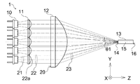
図1は、露光用光源装置の第一実施形態の構成例を模式的に示す図面である。露光用光源装置1は、複数の半導体レーザ光源10と、複数のコリメート光学系11と、集光光学系12と、光導波路13を備える。
[First embodiment]
FIG. 1 is a drawing schematically showing a configuration example of a first embodiment of an exposure light source device. The exposure
第一実施形態においては、光導波路13は円筒形状であり、図1においては、入射面14と直交する軸を光軸15とし、集光光学系12の光軸と一致するように配置されてる。また、光軸15方向をZ方向とし、Z方向に直交する平面をXY平面とし、入射面14に対する光の入射角をθ1とする。ここで、光導波路13は、具体的には光ファイバや円柱形状のガラス体等を用いることができる。
In the first embodiment, the
半導体レーザ光源10は、半導体レーザチップをケーシングしたレーザ光源である。半導体レーザ光源10は、光の出射窓の中心を主光線22aが通過するように、光を出射するレーザ光源である。
The semiconductor
図1に示すように、コリメート光学系11は、半導体レーザ光源10から出射された光線束21を、略平行の光線束22に変換して出射するコリメートレンズである。各半導体レーザ光源10に対応して複数のコリメート光学系11が配置されている。
As shown in FIG. 1, the collimating
図1に示すように、集光光学系12は、コリメート光学系11から出射された光線束22を、焦点位置に向かって集光する光線束23に変換して出射する集光レンズである。
As shown in FIG. 1, the condensing
図1に示す、光導波路13は、入射面14が、集光光学系12の焦点の位置になるように配置されている。ただし、本明細書では、「焦点位置に配置する」とは、完全に焦点の位置に一致する場合の他、焦点距離に対して光軸15に平行な方向に±10%の距離だけ移動した位置を含む概念であるものとする。なお、図1における光軸15とは、集光光学系12の入射面20に対して直交し、入射面20の中心を通る軸である。図1に示すように、本実施形態においては、集光光学系12の中心を通る軸は光軸15に一致するように配置されているが、光軸15と集光光学系12の中心を通る軸は一致していなくても構わない。
The
光導波路13は、入射面14から入射された光を、光軸15に対する入射角θ1の角度を保持したまま、光軸15を中心とした周方向の分布を均一化させて、出射面16から入射角θ1と同じ角度の出射角θ2(図2A参照)で出射する。
The
ここで、光導波路13に入射した光線束が、どのように変換されて出射されるかを説明する。図2Aは、YZ平面視において、光導波路13内を進行する光を模式的に示した図面である。図2Aに示すように、光導波路13は、入射された光を側面で繰り返し反射させながら、光線を出射面16へと導く。
Here, how the light flux incident on the
図2Aでは、模式的に一本の光線のみを表しているが、光導波路13には複数の光線束が入射され、光線が、光導波路13内に集約されて進行することによって、出射面16においてXY平面上の分布が均一化された光線束となって出射される。
In FIG. 2A, only one light beam is schematically shown, but a plurality of light beam bundles are incident on the
次に、光導波路13内を進行する光を、XY平面で見た場合を説明する。図2Bは、XY平面視において、光導波路13内を進行する光を模式的に示した図面である。図2Bに示すように、光導波路13に入射した光線束24は、円形である光導波路13の内壁面上で反射する。ここで、一定の幅を有する光線束24は、光導波路13の円形の内壁面上で反射すると、対向する壁面に向かって、幅が広がりながら進行する。
Next, a case where the light traveling in the
図2Cは、光導波路13から出射される光を模式的に示した図面である。光線束24は、光導波路13の内壁面上で反射を繰り返しながら進行し、やがて光導波路13の内壁面の周方向全体にわたって反射しながら進行する光線束24となる。出射面16に到達した光線束24は、光軸15を中心とした出射角θ2の円環状の光線束25として出射される。
FIG. 2C is a diagram schematically showing the light emitted from the
光導波路13から出射する光が、照度ムラを生じないためには、上述のように、光軸15を中心とする同心円上において、光が存在しない、又は主光線22a近傍と比較して、極めて光強度の低い領域が存在しないように光源や光学系の配置をする必要がある。
In order that the light emitted from the
第一実施形態においては、各半導体レーザ光源10は、同一平面上に配置されており、集光光学系12の入射面20上の光線束を、光軸15を中心に回転させて、同一の径方向30に向かって並べたときに、隣接する光線束の一部が重なるように配置されている。各コリメート光学系11も各半導体レーザ光源10に対応するように、同一平面上に配置されているが、半導体レーザ光源10もコリメート光学系11も、同一平面上に配置されていなくても構わない。
In the first embodiment, the semiconductor
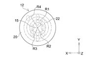
図3Aは、図1の集光光学系12を入射面20側からZ方向に向かって見たときの模式的な図面である。図3Bは、図3Aに示す集光光学系12の入射面20上の各光線束22を、仮想的に光軸15を中心に回転させて、同一の径方向30に向かって並べた状態を示す模式的な図面である。図3Bが示すように、同一の径方向30に向かって並べられた各光線束22は、隣接する光線束22の一部と重なっている。図3Bでは隣接する光線束22同士が重なっている領域がハッチングにて図示されている。
FIG. 3A is a schematic view of the condensing
図3Bにおいては、集光光学系12の入射面20において、光軸15を中心として回転させて、同一の径方向30に向かってに並べたときの隣接する光線束22の一部が重なり合っている。図3Cは、図3Bに示す集光光学系12の入射面20上で隣接する一組の光線束22を、拡大して示す図面である。図3Cに示すように、隣接する光線束22が集光光学系12の入射面20上において重なり合う領域L1の面積をS1とし、集光光学系12の入射面20上における光線束22の照射領域L2の面積をS2とした場合に、S1/S2の値は20%以上70%以下が好ましく、30%以上50%以下がより好ましい。他の隣接する光線束22同士の重なり合いについても同様である。
In FIG. 3B, in the
従って、集光光学系12から出射された角度分布のムラが抑えられた光線束は、光導波路13の入射面14に入射され、光軸15を中心とした周方向の分布が均一化されて、出射面16から出射される。
Therefore, the light flux emitted from the condensing
さらに、図3Aに示す例では、集光光学系12を入射面20上の光線束22に関し、光軸15から同一の距離に配置されている光線束群の数は、光軸に近い光線束群から順番に、第一半径R1の第1光線束群に属する数が4、第二半径R2の第2光線束群に属する数が3、第三半径R3の第3光線束群に属する数が2、第四半径R4の第4光線束群に属する数が1となっている。
Further, in the example shown in FIG. 3A, regarding the light collection
つまり、光軸15からの距離が同一の光線束群に属する数が、光軸15から離れるにつれて逓減している。従って、光導波路13の出射面16から出射される光は、出射角θ2が大きくなるほど光強度が逓減する角度分布を示す。これにより、図10に例示したように、光源装置を放電ランプとした場合の角度分布に近い角度分布を得ることができる。
That is, the numbers belonging to the bundle of light rays having the same distance from the
第一実施形態では、第4光線束群までの構成としているが、光線束群は、光軸15に最も近い光線束から順番に、第1光線束群、第2光線束群、第3光線束群、・・・、第n光線束群、・・・と、任意の数だけ構成されていてもよい。さらに当該構成において、光軸15からの距離がn番目に近い第n光線束群を基準として、光線束群に属する光線束の数が、光軸15から離れるにつれて逓減するものであっても構わない。なお、上述のとおり、nは任意の自然数である。
In the first embodiment, up to the fourth ray bundle group is configured, but the ray bundle groups are the first ray bundle group, the second ray bundle group, and the third ray bundle in order from the ray bundle closest to the
[第二実施形態]
本発明の露光用光源装置の第二実施形態の構成につき、第一実施形態と異なる箇所を中心に説明する。
[Second embodiment]
The configuration of the second embodiment of the exposure light source device of the present invention will be described focusing on the points different from the first embodiment.
図4Aは、露光用光源装置の別実施形態の構成例を模式的に示す図面である。図4Aに示す実施形態は、集光光学系12の入射面20に入射する光線束22は、Y方向において、光軸15よりも正方向側に入射する光線束22pと、負方向側に入射する光線束22mとに分けられる。光軸15とは非平行な方向に進行する光線束(22p,22m)は、ミラー40によって、光軸15に対して平行な方向に進行する光線束(22p,22m)に変換されて、集光光学系12の入射面20に入射される。
FIG. 4A is a drawing schematically showing a configuration example of another embodiment of the exposure light source device. In the embodiment shown in FIG. 4A, a bundle of
図4Aに示すように、第二実施形態では、光線束22pに係る半導体レーザ光源10pとコリメート光学系11pを、Y方向において光軸15に対して正方向、光線束22mに係る半導体レーザ光源10mとコリメート光学系11mを、Y方向において光軸15に対して負方向に、それぞれ対向する平面上に配置されているものとした。各半導体レーザ光源(10p,10m)と各コリメート光学系(11p,11m)は、それぞれ同一平面上に配置されていなくても構わない。
As shown in FIG. 4A, in the second embodiment, the semiconductor
図4Bは、図4Aの集光光学系を入射面側からZ方向に向かって見たときの模式的な図面である。ミラー40によって光軸15に平行に進行する光となった光線束(22p,22m)は、集光光学系12の入射面20に入射する。図4Bに示すように、各光線束(22p,22m)は、集光光学系12の入射面20において、光軸15を中心に回転させて、同一の径方向30に向かって並べたときに、隣接する光線束の一部が重なるように配置されている。
FIG. 4B is a schematic view of the condensing optical system of FIG. 4A when viewed from the incident surface side in the Z direction. The bundle of rays (22p, 22m) that has become a light traveling parallel to the
また、第二実施形態においても、集光光学系12を入射面20上の光線束22に関し、光軸15から同一の距離に配置されている光線束群の数は、中心が光軸15にある光線束22が1、次に光軸に近い順番で、第一半径R1の第1光線束群に属する数が4、第二半径R2の第2光線束群に属する数が3、第三半径R3の第3光線束群に属する数が2、第四半径R4の第4光線束群に属する数が1となっている。
Also in the second embodiment, regarding the bundle of
つまり、光軸15からの距離が同一の光線束群に属する数が、光軸15から離れるにつれて逓減している。従って、光導波路13の出射面16から出射される光は、出射角θ2が大きくなるほど光強度が逓減する角度分布を示す。これにより、図10に例示したように、光源装置を放電ランプとした場合の角度分布に近い角度分布を得ることができる。
That is, the numbers belonging to the bundle of light rays having the same distance from the
上述したような、放電ランプを用いた光源装置から出射される光の角度分布に近い光を出射する露光用光源装置1は、以下のように、露光装置の光源として利用することができる。
The exposure
図6は、露光装置70の構成を模式的に示す図面である。図6に示す露光装置70は、上述の第一実施形態の露光用光源装置1を備えているが、第二実施形態の露光用光源装置1を備えるものであっても構わない。そして、光導波路13の後段に、位置分布を均一化させるインテグレータ光学系71と投影光学系72及びマスク73を備え、必要に応じて投影レンズ74を備える。投影光学系72によって投影される位置にマスク73を設置し、マスク73の後段にマスク73のパターン像を焼き付ける対象となる感光性基板75を設置する。なお、インテグレータ光学系71には、例えばロッドインテグレータやフライアイレンズのような、入射した光の位置分布の均一性を向上させて出射する光学系が用いられる。
FIG. 6 is a drawing schematically showing the configuration of the
この状態で、光導波路13から光が出射されると、インテグレータ光学系71によって位置分布が均一化されて、投影光学系72に照射される。投影光学系72は、この光を、マスク73のパターン像を直接又は投影レンズ74を介して感光性基板75上に投影する。
In this state, when light is emitted from the
露光装置70は、上記各実施形態で説明した露光用光源装置1を備えることで、半導体レーザ光源を用いて、放電ランプを用いた光源装置から出射される光の角度分布に近い光を露光することができる。
The
[別実施形態]
以下、別実施形態について説明する。
[Another embodiment]
Hereinafter, another embodiment will be described.
〈1〉 図5は、露光用光源装置の別実施形態の構成例を模式的に示す図面である。図5が示すように、集光光学系12の入射面20において、楕円形状を呈する光線束22の長軸22Lが、光軸15側を向く楕円形状を呈している。
<1> FIG. 5 is a drawing schematically showing a configuration example of another embodiment of the exposure light source device. As shown in FIG. 5, on the
このような構成によれば、上述のように、集光光学系12の入射面20において、それぞれの光線束22は、光軸15を中心に回転させたときに、径方向30に沿うように長軸22L方向が揃うため、隣接する光線束22同士が重なりやすく、短軸22S方向でそろえる場合に比較して、隣接する光線束22を離間させることができる。従って、図1に示すような、隣接する半導体レーザ光源10や、隣接するコリメート光学系11をより疎に配置することができる。半導体レーザ光源10やコリメート光学系11が疎に配置できれば、それぞれの配置の自由度が高くなり、より配線しやすい構成等を採用することができる。
According to such a configuration, as described above, on the
〈2〉 図4Aに示すように、本発明の構成は集光光学系12の入射面20において、光軸15を中心に回転させて、同一の径方向30に向かって並べたときに、隣接する光線束22の一部が重なっており、光軸15からの距離が同一である光線束群に属する光線束の数が、光軸15からの距離が同一の光線束群に属する数が、光軸15から離れるにつれて逓減していればよく、半導体レーザ光源10とコリメート光学系11の配置は、上記実施形態には限られない。
<2> As shown in FIG. 4A, the configuration of the present invention is such that when the light is incident on the
例えば、露光用光源装置の一つの実施形態としては、半導体レーザ光源10から出射され、コリメート光学系11によって略平行光に変換された光線束22が入射する光ファイバを備えていてもよい。集光光学系12に入射した光線束22が、集光光学系12の入射面20上において、光軸15を中心に回転させて、同一の径方向30に向かって並べたときに、隣接する光線束22の一部が重なり、光軸15からの距離が同一の光線束群に属する数が、光軸15から離れるにつれて逓減するように、当該光ファイバの出射面が配置された構成であってもよい。
For example, one embodiment of the exposure light source device may include an optical fiber into which the
〈3〉 上記実施形態では、半導体レーザ光源10に含まれる半導体レーザチップは、図8を参照して説明した各半導体レーザチップ200と同様の、いわゆる「端面発光型」の構造である場合を想定して説明した。しかし、本発明は、各半導体レーザチップが、半導体層の積層方向に光が取り出される、いわゆる「面発光型」の構造であっても、同様に適用可能である。ただし、この場合には、集光光学系12の入射面20上に入射される光線束は、ほぼ真円形状を呈する。
<3> In the above-described embodiment, it is assumed that the semiconductor laser chip included in the semiconductor
1 : 光源装置
10,10p,10m : 半導体レーザ光源
11,11p,11m : コリメート光学系
12 : 集光光学系
13 : 光導波路
14 : 光導波路入射面
15 : 光軸
16 : 光導波路出射面
20 : 集光光学系入射面
21 : 光線束
22,22p,22m : 光線束
22a : 主光線
22L : 光線束の長軸
22S : 光線束の短軸
23 : 光線束
24 : 光線束
25 : 光線束
30 : 径方向
40 : ミラー
70 : 露光装置
71 : インテグレータ光学系
72 : 投影光学系
73 : マスク
74 : 投影レンズ
75 : 感光性基板
100 : 半導体レーザ光源
101 : コリメートレンズ
102 : 集光レンズ
103 : 集光レンズ入射面
104 : ロッドインテグレータ
105 : ロッドインテグレータ入射面
106 : ロッドインテグレータ出射面
110a,110b,110c : 主光線
111a,111b,111c : 主光線
121,121a,121b,121c : 光線束
122a,122b,122c : 光線束
123a,123b,123c : 光線束
130 : 領域
140 : 光軸
150 : 焦点位置
200 : 半導体レーザチップ
201 : エミッタ
θ1 : 入射角
θ2 : 出射角
α1,α2 : 入射角
R1 : 第一半径
R2 : 第二半径
R3 : 第三半径
R4 : 第四半径
L1 : 照射重複領域
L2 : 照射領域
S1,S2 : 面積
1: Light source device 10, 10p, 10m: Semiconductor laser light source 11, 11p, 11m: Collimating optical system 12: Condensing optical system 13: Optical waveguide 14: Optical waveguide incident surface 15: Optical axis 16: Optical waveguide emitting surface 20: Condensing optical system incident surface 21: Ray bundle 22, 22p, 22m: Ray bundle 22a: Chief ray 22L: Long axis of ray bundle 22S: Short axis of ray bundle 23: Ray bundle 24: Ray bundle 25: Ray bundle 30: Radial direction 40: Mirror 70: Exposure device 71: Integrator optical system 72: Projection optical system 73: Mask 74: Projection lens 75: Photosensitive substrate 100: Semiconductor laser light source 101: Collimator lens 102: Condenser lens 103: Condenser lens Incident surface 104: Rod integrator 105: Rod integrator incident surface 106: Rod integrator exit surface 110a, 110b, 110c: Chief rays 111a, 111b, 111c: Chief rays 121, 121a, 121b, 121c: Ray bundles 122a, 122b, 122c: Ray bundles 123a, 123b, 123c: Ray bundle 130: Region 140: Optical axis 150: Focus position 200: Semiconductor laser chip 201: Emitter θ1: Incident angle θ2: Exit angle α1, α2: Incident angle R1: First radius R2: Second radius R3: Third radius R4: Fourth radius L1: Irradiation overlapping area L2: Irradiation area S1, S2: Area
Claims (5)
前記複数の半導体レーザ光源に対応して配置され、前記半導体レーザ光源から出射された光線束を、略平行の光線束に変換して出射する、複数のコリメート光学系と、
前記コリメート光学系から出射された光線束が入射される入射面を含み、前記コリメート光学系から出射された光線束を集光する集光光学系と、
前記集光光学系から出射された光線束が集光する位置に配置された、円形状の入射面を含む光導波路とを備え、
前記集光光学系の入射面における、前記複数の半導体レーザ光源から出射されたそれぞれの光線束は、仮想的に前記集光光学系の光軸を中心に回転させて、同一の径方向に向かって並べたときに、隣接する光線束の一部が重なっており、
前記複数の半導体レーザ光源は、前記集光光学系の入射面において、前記集光光学系の光軸からの距離が同一である光線束群に属する光線束の数が、光軸からの距離がn番目に近い第n光線束群を基準として、光軸から離れるにつれて逓減するように配置されていることを特徴とする露光用光源装置。 A plurality of semiconductor laser light sources,
A plurality of collimating optical systems, which are arranged corresponding to the plurality of semiconductor laser light sources, convert the light flux emitted from the semiconductor laser light source into a substantially parallel light flux, and emit the light.
A condensing optical system that includes an incident surface on which the light flux emitted from the collimating optical system is incident, and that condenses the light flux emitted from the collimating optical system,
An optical waveguide including a circular incident surface, which is arranged at a position where a bundle of rays emitted from the condensing optical system is condensed,
The respective light fluxes emitted from the plurality of semiconductor laser light sources on the entrance surface of the condensing optical system are virtually rotated about the optical axis of the condensing optical system and are directed in the same radial direction. When arranged side by side, some of the adjacent ray bundles overlap,
In the plurality of semiconductor laser light sources, on the incident surface of the condensing optical system, the number of ray bundles belonging to the bundle of ray bundles having the same distance from the optical axis of the condensing optical system is the distance from the optical axis. An exposure light source device, wherein the light source device for exposure is arranged so as to gradually decrease with distance from the optical axis, with an n-th ray bundle group close to the n-th reference.
The light source device for exposure according to any one of claims 1 to 4, further comprising an integrator optical system that homogenizes a position distribution of a light beam emitted from the optical waveguide and emits the light beam.
Priority Applications (3)
| Application Number | Priority Date | Filing Date | Title |
|---|---|---|---|
| JP2018228553A JP2020091402A (en) | 2018-12-05 | 2018-12-05 | Light source device for exposure |
| TW108139629A TW202032279A (en) | 2018-12-05 | 2019-11-01 | Light source device for exposure |
| PCT/JP2019/043595 WO2020116081A1 (en) | 2018-12-05 | 2019-11-07 | Light source device for exposure |
Applications Claiming Priority (1)
| Application Number | Priority Date | Filing Date | Title |
|---|---|---|---|
| JP2018228553A JP2020091402A (en) | 2018-12-05 | 2018-12-05 | Light source device for exposure |
Publications (1)
| Publication Number | Publication Date |
|---|---|
| JP2020091402A true JP2020091402A (en) | 2020-06-11 |
Family
ID=70973594
Family Applications (1)
| Application Number | Title | Priority Date | Filing Date |
|---|---|---|---|
| JP2018228553A Pending JP2020091402A (en) | 2018-12-05 | 2018-12-05 | Light source device for exposure |
Country Status (3)
| Country | Link |
|---|---|
| JP (1) | JP2020091402A (en) |
| TW (1) | TW202032279A (en) |
| WO (1) | WO2020116081A1 (en) |
Cited By (1)
| Publication number | Priority date | Publication date | Assignee | Title |
|---|---|---|---|---|
| US12669114B2 (en) | 2022-06-22 | 2026-06-30 | Uif (University Industry Foundation, Yonsei University | Energy-efficient electromagnetic micropump system |
Family Cites Families (4)
| Publication number | Priority date | Publication date | Assignee | Title |
|---|---|---|---|---|
| US6137631A (en) * | 1999-03-12 | 2000-10-24 | Kodak Polychrome Graphics Llc | Illumination system and method for spatial modulators |
| JP2003345030A (en) * | 2002-05-23 | 2003-12-03 | Fuji Photo Film Co Ltd | Exposure device |
| EP1771927A1 (en) * | 2004-06-01 | 2007-04-11 | Trumpf Photonics, Inc. | Optimum matching of the output of a two-dimensional laser array stack to an optical fiber |
| US7881355B2 (en) * | 2005-12-15 | 2011-02-01 | Mind Melters, Inc. | System and method for generating intense laser light from laser diode arrays |
-
2018
- 2018-12-05 JP JP2018228553A patent/JP2020091402A/en active Pending
-
2019
- 2019-11-01 TW TW108139629A patent/TW202032279A/en unknown
- 2019-11-07 WO PCT/JP2019/043595 patent/WO2020116081A1/en not_active Ceased
Cited By (1)
| Publication number | Priority date | Publication date | Assignee | Title |
|---|---|---|---|---|
| US12669114B2 (en) | 2022-06-22 | 2026-06-30 | Uif (University Industry Foundation, Yonsei University | Energy-efficient electromagnetic micropump system |
Also Published As
| Publication number | Publication date |
|---|---|
| WO2020116081A1 (en) | 2020-06-11 |
| TW202032279A (en) | 2020-09-01 |
Similar Documents
| Publication | Publication Date | Title |
|---|---|---|
| JP4059623B2 (en) | Illumination device and uniform illumination device | |
| JP6238140B2 (en) | Illumination optical unit for projection exposure apparatus | |
| JPH032284B2 (en) | ||
| JP6172540B2 (en) | Light source device | |
| TW201115279A (en) | Laser exposure apparatus | |
| JP6806236B2 (en) | Lighting equipment and methods, exposure equipment and methods, and device manufacturing methods | |
| WO2020116081A1 (en) | Light source device for exposure | |
| JP5220136B2 (en) | Illumination optical system, exposure apparatus, and device manufacturing method | |
| JP6315720B2 (en) | Exposure illumination device | |
| JP2008249454A (en) | Illumination optical apparatus and sample inspection apparatus | |
| WO2016152359A1 (en) | Light source device and exposure device | |
| WO2017138523A1 (en) | Light source device | |
| JPS622539A (en) | Illumination optical system | |
| JP2020091399A (en) | Light source device for exposure | |
| JP7068659B2 (en) | Light source device for exposure | |
| JP5843905B2 (en) | Illumination optical system, exposure apparatus, and device manufacturing method | |
| JP2006208682A (en) | Lighting optical device and optical device | |
| CN117501183A (en) | Illumination optical system and exposure device | |
| JP3952867B2 (en) | Laser concentrator | |
| TWI625606B (en) | Illumination optical unit for euv projection lithography | |
| CN215067713U (en) | Illumination system for a lithographic apparatus and lithographic apparatus | |
| CN111443494B (en) | Light source device | |
| JPH10129033A (en) | Multi-beam recorder | |
| JPH0568846B2 (en) | ||
| JP2022087705A (en) | Scanning exposure equipment and article manufacturing method |