JP2020101427A - Inspection jig, manufacturing method of inspection jig, and inspection device including inspection jig - Google Patents
Inspection jig, manufacturing method of inspection jig, and inspection device including inspection jig Download PDFInfo
- Publication number
- JP2020101427A JP2020101427A JP2018239188A JP2018239188A JP2020101427A JP 2020101427 A JP2020101427 A JP 2020101427A JP 2018239188 A JP2018239188 A JP 2018239188A JP 2018239188 A JP2018239188 A JP 2018239188A JP 2020101427 A JP2020101427 A JP 2020101427A
- Authority
- JP
- Japan
- Prior art keywords
- inspection
- support
- wall surface
- probe
- hole portion
- Prior art date
- Legal status (The legal status is an assumption and is not a legal conclusion. Google has not performed a legal analysis and makes no representation as to the accuracy of the status listed.)
- Pending
Links
- 238000007689 inspection Methods 0.000 title claims abstract description 228
- 238000004519 manufacturing process Methods 0.000 title claims description 11
- 239000000523 sample Substances 0.000 claims abstract description 101
- 238000012545 processing Methods 0.000 claims description 31
- 238000000034 method Methods 0.000 claims description 14
- 238000005304 joining Methods 0.000 claims description 11
- 230000002093 peripheral effect Effects 0.000 claims description 6
- 230000001678 irradiating effect Effects 0.000 claims description 4
- 239000000758 substrate Substances 0.000 abstract description 11
- 239000004065 semiconductor Substances 0.000 description 8
- 238000006073 displacement reaction Methods 0.000 description 6
- 238000012986 modification Methods 0.000 description 5
- 230000004048 modification Effects 0.000 description 5
- 230000015572 biosynthetic process Effects 0.000 description 4
- 238000005452 bending Methods 0.000 description 3
- 230000000149 penetrating effect Effects 0.000 description 3
- 238000009434 installation Methods 0.000 description 2
- 230000002452 interceptive effect Effects 0.000 description 2
- 238000002955 isolation Methods 0.000 description 2
- 239000000463 material Substances 0.000 description 2
- 238000003825 pressing Methods 0.000 description 2
- 238000009751 slip forming Methods 0.000 description 2
- 238000012360 testing method Methods 0.000 description 2
- 239000004593 Epoxy Substances 0.000 description 1
- 238000013459 approach Methods 0.000 description 1
- 239000000919 ceramic Substances 0.000 description 1
- 238000005553 drilling Methods 0.000 description 1
- 239000011521 glass Substances 0.000 description 1
- 238000003780 insertion Methods 0.000 description 1
- 230000037431 insertion Effects 0.000 description 1
- 239000004973 liquid crystal related substance Substances 0.000 description 1
- 238000003754 machining Methods 0.000 description 1
- 230000013011 mating Effects 0.000 description 1
- 238000003672 processing method Methods 0.000 description 1
- 229910052710 silicon Inorganic materials 0.000 description 1
- 239000010703 silicon Substances 0.000 description 1
- 229910000679 solder Inorganic materials 0.000 description 1
Images


Classifications
-
- G—PHYSICS
- G01—MEASURING; TESTING
- G01R—MEASURING ELECTRIC VARIABLES; MEASURING MAGNETIC VARIABLES
- G01R31/00—Arrangements for testing electric properties; Arrangements for locating electric faults; Arrangements for electrical testing characterised by what is being tested not provided for elsewhere
- G01R31/28—Testing of electronic circuits, e.g. by signal tracer
- G01R31/2851—Testing of integrated circuits [IC]
-
- G—PHYSICS
- G01—MEASURING; TESTING
- G01R—MEASURING ELECTRIC VARIABLES; MEASURING MAGNETIC VARIABLES
- G01R1/00—Details of instruments or arrangements of the types included in groups G01R5/00 - G01R13/00 and G01R31/00
- G01R1/02—General constructional details
- G01R1/06—Measuring leads; Measuring probes
- G01R1/067—Measuring probes
- G01R1/06711—Probe needles; Cantilever beams; "Bump" contacts; Replaceable probe pins
- G01R1/06716—Elastic
- G01R1/06722—Spring-loaded
-
- G—PHYSICS
- G01—MEASURING; TESTING
- G01R—MEASURING ELECTRIC VARIABLES; MEASURING MAGNETIC VARIABLES
- G01R1/00—Details of instruments or arrangements of the types included in groups G01R5/00 - G01R13/00 and G01R31/00
- G01R1/02—General constructional details
- G01R1/04—Housings; Supporting members; Arrangements of terminals
- G01R1/0408—Test fixtures or contact fields; Connectors or connecting adaptors; Test clips; Test sockets
-
- G—PHYSICS
- G01—MEASURING; TESTING
- G01R—MEASURING ELECTRIC VARIABLES; MEASURING MAGNETIC VARIABLES
- G01R1/00—Details of instruments or arrangements of the types included in groups G01R5/00 - G01R13/00 and G01R31/00
- G01R1/02—General constructional details
- G01R1/06—Measuring leads; Measuring probes
- G01R1/067—Measuring probes
- G01R1/073—Multiple probes
- G01R1/07307—Multiple probes with individual probe elements, e.g. needles, cantilever beams or bump contacts, fixed in relation to each other, e.g. bed of nails fixture or probe card
- G01R1/07364—Multiple probes with individual probe elements, e.g. needles, cantilever beams or bump contacts, fixed in relation to each other, e.g. bed of nails fixture or probe card with provisions for altering position, number or connection of probe tips; Adapting to differences in pitch
- G01R1/07371—Multiple probes with individual probe elements, e.g. needles, cantilever beams or bump contacts, fixed in relation to each other, e.g. bed of nails fixture or probe card with provisions for altering position, number or connection of probe tips; Adapting to differences in pitch using an intermediate card or back card with apertures through which the probes pass
-
- G—PHYSICS
- G01—MEASURING; TESTING
- G01R—MEASURING ELECTRIC VARIABLES; MEASURING MAGNETIC VARIABLES
- G01R3/00—Apparatus or processes specially adapted for the manufacture or maintenance of measuring instruments, e.g. of probe tips
-
- G—PHYSICS
- G01—MEASURING; TESTING
- G01R—MEASURING ELECTRIC VARIABLES; MEASURING MAGNETIC VARIABLES
- G01R31/00—Arrangements for testing electric properties; Arrangements for locating electric faults; Arrangements for electrical testing characterised by what is being tested not provided for elsewhere
- G01R31/26—Testing of individual semiconductor devices
- G01R31/2601—Apparatus or methods therefor
-
- G—PHYSICS
- G01—MEASURING; TESTING
- G01R—MEASURING ELECTRIC VARIABLES; MEASURING MAGNETIC VARIABLES
- G01R1/00—Details of instruments or arrangements of the types included in groups G01R5/00 - G01R13/00 and G01R31/00
- G01R1/02—General constructional details
- G01R1/06—Measuring leads; Measuring probes
- G01R1/067—Measuring probes
- G01R1/073—Multiple probes
- G01R1/07307—Multiple probes with individual probe elements, e.g. needles, cantilever beams or bump contacts, fixed in relation to each other, e.g. bed of nails fixture or probe card
Landscapes
- Physics & Mathematics (AREA)
- General Physics & Mathematics (AREA)
- Engineering & Computer Science (AREA)
- Computer Hardware Design (AREA)
- Microelectronics & Electronic Packaging (AREA)
- General Engineering & Computer Science (AREA)
- Measuring Leads Or Probes (AREA)
Abstract
Description
本発明は、検査対象の検査に用いられる検査治具、この検査治具の製造方法、及び検査治具を備えた検査装置に関する。 The present invention relates to an inspection jig used to inspect an inspection target, a method for manufacturing the inspection jig, and an inspection device including the inspection jig.
従来、先端が検査対象に接触するとともに、ワイヤ状に形成され屈曲可能で弾性を有する複数のプローブと、上記プローブの先端側部分を支持する先端側支持体と、上記先端側支持体の後方に所定の隙間を介して配置された後端側支持体とを備えた検査治具が知られている(例えば、特許文献1参照)。 Conventionally, a plurality of probes which are formed into a wire shape and have flexibility and elasticity while the tip is in contact with an object to be inspected, a tip side support body which supports a tip side portion of the probe, and a rear side of the tip side support body are provided. An inspection jig including a rear end side support body arranged with a predetermined gap is known (for example, refer to Patent Document 1).
この検査治具は、先端側支持体に形成された先端側挿通孔を貫通したプローブの一端部を、基板の被検査部に当接させるとともに、後端側支持体に支持されたプローブの後端部を、電極板の電極に当接させた状態で、検査対象の電気的特性を測定することにより、その良否判定を行うように構成されている。 This inspection jig makes one end of the probe penetrating the tip side insertion hole formed in the tip side support contact the portion to be inspected of the substrate, and the rear end of the probe supported by the rear side support. The end of the electrode plate is brought into contact with the electrode of the electrode plate, and the electrical characteristics of the inspection target are measured to make a pass/fail judgment.
上述のプローブを被検査部に正しく接触させるためには、先端側支持体及び後端側支持体によりプローブを安定して支持させる必要がある。特に、先端側支持体にはプローブから大きな力が作用するため、先端側支持体の板厚を十分に大きくすることにより、先端側支持体の変形を抑制し、プローブを安定して支持させることが望ましい。 In order to bring the above probe into proper contact with the portion to be inspected, it is necessary to stably support the probe by the front end side support and the rear end side support. In particular, since a large force acts on the tip side support from the probe, it is possible to suppress the deformation of the tip side support and to stably support the probe by making the plate thickness of the tip side support sufficiently large. Is desirable.
プローブの直径は極めて小さいので、これに対応した細径のドリルを使用して先端側支持体に細径のプローブ支持孔を形成しなければならない。この場合に、先端側支持体の板厚が大きいと、ドリルを貫通させることは困難であった。 Since the diameter of the probe is extremely small, it is necessary to form a small-diameter probe support hole in the tip-side support by using a small-diameter drill corresponding to the diameter. In this case, if the plate thickness of the tip side support body is large, it was difficult to penetrate the drill.
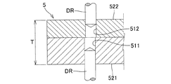
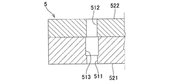
このため、例えば図9に示すように、複数枚の支持板521,522に下部ドリル孔511及び上部ドリル孔512をそれぞれ個別に形成し、これらを重ね合わせてプローブの先端側部分を支持する支持体5を形成することが行われている。これにより、ドリルの曲り等を抑制しつつ、板厚Tの大きい支持体5に細径のプローブ支持孔を形成することができる。しかし、複数枚の支持板521,522を重ね合わせて支持体5を構成する際に、下部ドリル孔511及び上部ドリル孔512の軸心に位置ずれが発生する可能性がある。したがって、支持体5にプローブを支持させる際に、プローブの引っ掛かり等が生じ易い。
Therefore, for example, as shown in FIG. 9, a
なお、下部ドリル孔511及び上部ドリル孔512の軸心に位置ずれが生じることに起因したプローブの引っ掛かり等を防止するため、例えば図10に示すように、下方に位置する支持板521に、大径の中間部ドリル孔513を、さらに設けることも考えられる。
In order to prevent the probe from being caught due to the displacement of the axial centers of the
すなわち、上方の支持板522に小径の上部ドリル孔512の加工を施すとともに、下方の支持板521に小径の下部ドリル孔511と、大径の中間部ドリル孔513の加工とを別々に施すことも考えられる。しかし、この場合には、三回の孔加工が必要となって、検査治具の生産性を向上させることができないという懸念がある。
That is, the
本発明の目的は、生産性を向上することが可能な検査治具、この検査治具の製造方法、及び検査治具を提供することである。 An object of the present invention is to provide an inspection jig capable of improving productivity, a method of manufacturing the inspection jig, and an inspection jig.
本発明の一例に係る検査治具は、一端部が検査対象に圧接される棒状のプローブと、前記プローブを支持する支持孔を有する板状の第一支持体とを備え、前記支持孔は、前記第一支持体の一壁面側から前記第一支持体の板厚方向中間部側に近づくにしたがって拡径する第一テーパ孔部を備えている。 An inspection jig according to an example of the present invention includes a rod-shaped probe whose one end is pressed against an inspection target, and a plate-shaped first support having a support hole for supporting the probe, the support hole, The first support has a first tapered hole portion whose diameter increases from one wall surface side toward the intermediate portion side in the plate thickness direction of the first support body.
また、本発明の一例に係る検査治具の製造方法は、前記第一支持板に前記第一テーパ孔部を形成する第一テーパ孔部形成工程と、前記第一支持板と前記第二支持板とを重ね合わせて接合する接合工程とを含んでいる。 In addition, a method of manufacturing an inspection jig according to an example of the present invention includes a first taper hole forming step of forming the first taper hole in the first support plate, the first support plate and the second support. And a joining step of joining the plates by overlapping them.
また、本発明の一例に係る検査装置は、上述の検査治具と、プローブの後端部に対して電気的に接続されるとともに、このプローブの後端部に電気信号を与えて検査対象の検査を行う検査部とを備えている。 In addition, the inspection device according to an example of the present invention is electrically connected to the above-described inspection jig and the rear end portion of the probe, and applies an electric signal to the rear end portion of the probe to inspect the inspection target. An inspection unit for performing inspection is provided.
このような構成の検査治具、この検査治具の製造方法、及び検査治具を備えた検査装置は、検査治具及び検査装置の生産性を向上することが可能である。 The inspection jig having such a configuration, the method for manufacturing the inspection jig, and the inspection device including the inspection jig can improve the productivity of the inspection jig and the inspection device.
以下、本発明に係る実施形態を図面に基づいて説明する。なお、各図において同一の符号を付した構成は、同一の構成であることを示し、その説明を省略する。
(第一実施形態)
Hereinafter, embodiments according to the present invention will be described with reference to the drawings. In addition, in each of the drawings, the components having the same reference numerals indicate the same components, and the description thereof will be omitted.
(First embodiment)
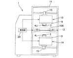
図1に示す検査装置1は、筐体11を有している。筐体11の内部空間には、検査対象固定装置12と、第一検査部13と、第二検査部14とが設けられている。検査対象固定装置12は、基板等からなる検査対象100を所定の位置に固定するように構成されている。
The inspection device 1 shown in FIG. 1 has a
検査対象100は、例えばガラスエポキシ基板、フレキシブル基板、セラミック多層配線基板、液晶ディスプレイやプラズマディスプレイ用の電極板、タッチパネル用等の透明導電板、及び半導体パッケージ用のパッケージ基板やフィルムキャリア等種々の基板であってもよい。検査対象100には、配線パターンや半田バンプ等の被検査部が形成されている。
The
第一検査部13は、検査対象固定装置12に固定された検査対象100の上方に位置する。第二検査部14は、検査対象固定装置12に固定された検査対象100の下方に位置する。第一検査部13及び第二検査部14は、検査対象100に形成された回路パターンを検査するための検査治具4U,4Lを備えている。検査治具4U,4Lには、複数のプローブ3が取り付けられている。また、第一検査部13及び第二検査部14は、筐体11内で適宜移動するための検査部移動機構15を備えている。
The
検査装置1は、検査対象固定装置12、第一検査部13、及び第二検査部14等の動作を制御する制御部20を備えている。制御部20は、例えばマイクロコンピュータを用いて構成されている。制御部20は、第一検査部13及び第二検査部14を適宜移動させ、検査対象固定装置12に固定された検査対象100に検査治具4U,4Lのプローブ3を接触させることにより、検査対象100の回路パターンを検査するように構成されている。検査治具4U,4Lは、同様に構成されているので、以下、検査治具4U,4Lを総称して検査治具4と称する。
The inspection device 1 includes a
なお、検査装置1は、基板を検査する基板検査装置に限られず、例えばシリコンなどの半導体基板に、複数の半導体チップに対応する回路が形成された半導体ウェハ、半導体チップ、CSP(Chip size package)、半導体素子(IC:Integrated Circuit)等の電子部品を検査するための半導体検査装置であってもよい。また、検査治具4は、半導体ウェハに複数のプローブ3を接触させて検査するためのいわゆるプローブカードであってもよい。
The inspection device 1 is not limited to a substrate inspection device for inspecting a substrate, and a semiconductor wafer, a semiconductor chip, a CSP (Chip size package) in which circuits corresponding to a plurality of semiconductor chips are formed on a semiconductor substrate such as silicon. A semiconductor inspection device for inspecting an electronic component such as a semiconductor element (IC: Integrated Circuit) may be used. The
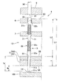
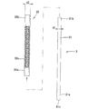
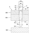
検査治具4は、図2に示すように、導電性を有する棒状のプローブ3と、複数本のプローブ3を支持する支持部材10とを備えている。プローブ3は、図3に示すように、例えば30μm程度の外径d1を有する棒状に形成された導電性部材からなる棒状体31と、この棒状体31に外嵌される導電性部材からなる筒状体32とを備えている。
As shown in FIG. 2, the
棒状体31の一端部31aには、検査対象100の被検査部101に当接する半球状の先端接触部31cが形成されている。なお、先端接触部31cは、半球状に限られず、先窄まりの円錐台状、もしくは円錐状、又は平坦面状等であってもよい。
A hemispherical
筒状体32は、円筒形状の一端部32aと、円筒形状の他端部32bとを有している。また、筒状体32の一端部32aと他端部32bとの間には、螺旋形状のばね部32cが設けられている。
The
棒状体31の本体部分が筒状体32内に挿入されるとともに、筒状体32の一端部32aが棒状体31の一端部にカシメ加工される等により固着されている。そして、図2に示すように、筒状体32外に突出する棒状体31の一端部31aの突出長さlaが一定となった状態で、棒状体31の一端部31aと筒状体32の一端部32aとが相連結されている。なお、棒状体31の一端部31aに設けられた大径の膨出部が、筒状体32の一端部32a内に圧入される等により、棒状体31と筒状体32とが相連結された構成であってもよい。
The main body of the rod-shaped
図2の上方側に位置する棒状体31の他端部31bは、筒状体32の他端部32bから所定距離だけ筒状体32内に入り込んだ位置に配置されている。棒状体31の他端部31bの入り込み量は、後述する検査対象100の検査時に圧縮されて弾性変形する筒状体32の変形量よりも大きな値に設定されている。これにより、検査対象100の検査時に筒状体32が圧縮されて変形した場合においても、棒状体31の他端部31bが筒状体32から突出した状態となることが防止されている。
The
支持部材10は、図2の下方部に位置する検査対象100に対向して配置される検査側支持体5からなる第一支持体を有している。また、支持部材10は、図2の上方側に配置される電極側支持体6と、検査側支持体5及び電極側支持体6の間に配置される中間部支持体7とからなる第二支持体を有している。検査側支持体5、電極側支持体6及び中間部支持体7は、それぞれ所定距離を隔てて相対向した状態で、例えば図略の連結部材を介して互いに連結されている。
The
検査側支持体5には、電極側支持体6及び中間部支持体7に比べてプローブ3から大きな力が作用する。このため、検査側支持体5の板厚は、電極側支持体6及び中間部支持体7よりも大きな値とされている。
A larger force is applied to the inspection-
検査側支持体5は、検査対象100に対向した対向壁面5Aを有する第一支持板501と、対向壁面5Aの反対側、つまり図2の上方側に位置する反対壁面5Bを有する第二支持板502とを備えている。第一支持板501と第二支持板502とが、互いに接着もしくは溶着され、又は連結ボルト等を介して一体に接合されることにより、検査側支持体5が構成される。
The inspection
なお、当実施形態では、第一支持板501の板厚が、第二支持板502よりも大きく形成された例について説明したが、逆に第二支持板502の板厚が、第一支持板501よりも大きくてもよい。また、第一支持板501の板厚と、第二支持板502の板厚とが同一であってもよい。
In the present embodiment, an example in which the plate thickness of the
図4に示すように、第一支持板501には、検査側支持体5の一壁面、つまり対向壁面5A側から、検査側支持体5の板厚方向中間部5C側に近づくにしたがって拡径する第一テーパ孔部53が形成されている。一方、第二支持板502には、上述の一壁面の反対側に位置する検査側支持体5の他壁面、つまり反対壁面5B側から、検査側支持体5の板厚方向中間部5C側に近づくにしたがって拡径する第二テーパ孔部54が形成されている。
As shown in FIG. 4, the diameter of the
そして、第一支持板501と第二支持板502とを重ね合わせて検査側支持体5を構成する際に、第一テーパ孔部53の軸心J1と、第二テーパ孔部54の軸心J2とを一致させるように位置合わせして、第一支持板501と第二支持板502とを接合する。これにより、第一テーパ孔部53と第二テーパ孔部54とを備えた支持孔51が検査側支持体5に形成される。
Then, when the
検査側支持体5の対向壁面5Aに位置する支持孔51の開口部、つまり第一テーパ孔部53の下端開口部55は、検査対象100の被検査部101に対向した位置に配置されている。また、第一テーパ孔部53の下端開口部55の直径D1は、棒状体31の外径d1よりもやや大きい。
The opening of the
検査側支持体5の反対壁面5Bに位置する支持孔51の開口部の直径、つまり第二テーパ孔部54の上端開口部56の直径D2は、棒状体31の外径d1よりもやや大きく、かつプローブ3の筒状体32の外径d2よりも小さい。
The diameter of the opening of the
例えば、棒状体31の外径d1が30μmで、筒状体32の外径d2が45μmである場合に、上端開口部56の直径D2は、35μm程度に形成されている。これにより、棒状体31の一端部31aが、支持孔51に挿入可能に構成されている。また、筒状体32の一端部32aが、検査側支持体5の反対壁面5Bに当接して係止され、支持孔51内に入り込むことが防止されている。
For example, when the outer diameter d1 of the rod-shaped
検査側支持体5の板厚方向中間部5Cに位置する支持孔51の直径、具体的には、第一支持板501と第二支持板502との合わせ面に位置する第一テーパ孔部53及び第二テーパ孔部54の境界部の直径D3は、相隣接する支持孔51,51の設置間隔、つまり複数の支持孔51,51の配列ピッチPよりも小さい値とされている。
The diameter of the
例えば、支持孔51,51の配列ピッチPが50μmである場合に、板厚方向中間部5Cに位置する支持孔51の直径D3は、この配列ピッチPよりも小さい値である45μm程度に設定されている。これにより、相隣接する支持孔51,51が互いに干渉することが防止され、各支持孔51の間に隔離壁57が設けられるようになっている。
For example, when the arrangement pitch P of the support holes 51, 51 is 50 μm, the diameter D3 of the support holes 51 located in the plate thickness direction
検査側支持体5に複数の支持孔51,51を形成する際に、相隣接する支持孔51,51の間には、例えば4μm程度の設置誤差が生じる可能性がある。この場合においても、相隣接する支持孔51,51が互いに干渉しないようにするには、板厚方向中間部5Cに位置する支持孔51の直径D3を、支持孔51,51の配列ピッチPよりも4μm以上小さい値とする必要がある。
When forming the plurality of support holes 51, 51 in the inspection-
なお、第一テーパ孔部53が形成された第一支持板501と、第二テーパ孔部54が形成された第二支持板502とを重ね合わせる際に、位置合わせ誤差が生じる可能性がある。この位置合わせ誤差に起因して、第一テーパ孔部53の軸心J1と第二テーパ孔部54の軸心J2との間に位置ずれが生じる場合がある(図11参照)。この場合においても、棒状体31の一端部31aを支持孔51に挿入する際に引っ掛かり等が生じないように、板厚方向中間部5Cに位置する支持孔51の直径D3が、下端開口部55の直径D1及び上端開口部56のD2よりもそれぞれ大きく形成されている。
A positioning error may occur when the
第一支持板501は、例えば320μm程度の厚みを有している。一方、第二支持板502は、例えば500μm程度の厚みを有している。また、検査側支持体5の板厚Tは、筒状体32外に突出した棒状体31の一端部31aの突出長さlaよりも小さい値、例えば突出長さlaの80%前後に設定されている。すなわち、棒状体31の一端部31aの突出長さlaが1000μmである場合に、検査側支持体5の板厚Tが、820μm程度に設定されている。
The
これにより、プローブ3を支持部材10に支持させた際に、図2に示すように、検査側支持体5の対向壁面5Aから突出した棒状体31の一端部31aの突出距離lbが、180μmとなる。また、上述のように検査側支持体5の板厚Tが、一端部31aの突出長さlaの80%程度に設定されることにより、検査側支持体5の板厚Tが十分な値に確保されている。この結果、後述のように検査側支持体5に圧接される筒状体32の一端部32aが安定して支持される。
As a result, when the
第一テーパ孔部53及び第二テーパ孔部54を備えた検査治具の製造方法を、図5及び図6に基づいて以下に説明する。この検査治具の製造方法は、第一支持板501に第一テーパ孔部53を形成する第一テーパ孔部形成工程と、第二支持板502に第二テーパ孔部54を形成する第二テーパ孔部形成工程と、第一支持板501と第二支持板502とを重ね合わせて接合する接合工程とを含んでいる。
A method of manufacturing the inspection jig including the first
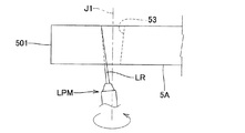
第一テーパ孔部形成工程では、まず、図5に示すように、第一支持板501の下方側にレーザ加工機LPMを配置し、レーザ加工機LPMから照射されるレーザ光LRの照射方向を、第一テーパ孔部53の周壁面に沿わせるようにセットする。
In the first taper hole forming step, first, as shown in FIG. 5, the laser processing machine LPM is arranged below the
そして、レーザ加工機LPMから第一支持板501の下面(対向壁面5A)に向けてレーザ光LRを照射しつつ、第一テーパ孔部53の軸心J1を中心に、レーザ加工機LPMを一回転以上、旋回させる。これにより、対向壁面5A側から検査側支持体5の板厚方向中間部5C側に近づくにしたがって拡径する第一テーパ孔部53が第一支持板501に形成される(図4参照)。
Then, while irradiating the laser beam LR from the laser processing machine LPM toward the lower surface (opposing
第二テーパ孔部形成工程では、図6に示すように、第二支持板502の上方側にレーザ加工機LPMを配置し、レーザ加工機LPMから照射されるレーザ光LRの照射方向を、第二テーパ孔部54の周壁面に沿わせるようにセットする。
In the second taper hole forming step, as shown in FIG. 6, the laser processing machine LPM is arranged above the
そして、第一テーパ孔部53の形成方法と同様にして、レーザ加工機LPMからレーザ光LRを、第二支持板502の上面(反対壁面5B)に向けて照射つつ、支持孔51の軸心J2を中心に、レーザ加工機LPMを旋回させる。これにより、反対壁面5B側から検査側支持体5の板厚方向中間部5C側に近づくにしたがって拡径する第二テーパ孔部54が第二支持板502に形成される。
Then, similar to the method of forming the first
次いで、接合工程において、第一テーパ孔部53の軸心J1と、第二テーパ孔部54の軸心J2とを一致させるように位置合わせした後、第一支持板501と第二支持板502とを重ね合わせて接合することにより、図4に示すように、検査側支持体5が構成される。
Next, in the joining step, the
なお、第一テーパ孔部53及び第二テーパ孔部54の形成方法は、上述のレーザ加工機LPMを使用した加工方法に限られない。例えば、テーパリーマ等を使用して、第一支持板501に第一テーパ孔部53を形成し、かつ第二支持板502に第二テーパ孔部54を形成してもよい。また、3Dプリンタを使用して検査側支持体5を形成する際に、第一テーパ孔部53及び第二テーパ孔部54を同時に形成することも可能である。
The method of forming the first
上述の実施形態では、第一支持板501の板厚を500μmに設定し、かつ第二支持板502の板厚を320μmに設定しているが、これには限られない。第一支持板501及び第二支持板502の板厚を同じ値、例えば400μmとしてもよい。
In the above-described embodiment, the plate thickness of the
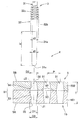
支持部材10を構成する電極側支持体6は、図2の上方部に位置する電極板9と対向するように設置された板状体からなっている。電極側支持体6には、その板厚方向に貫通するストレート孔からなるプローブ支持孔61が形成されている。このプローブ支持孔61は、その口径が筒状体の32の外径d2よりも大きな値に設定されている。そして、プローブ3の後端部、具体的には筒状体32の他端部32bが、プローブ支持孔61に挿入されて、支持されるように構成されている。
The electrode-
なお、電極板9には、導電線90が設けられ、その端面によりプローブ3の後端部が当接する電極91が構成されている。
A
中間部支持体7は、検査側支持体5と電極側支持体6との間に配置された板状体からなっている。中間部支持体7には、その板厚方向に貫通するストレート孔からなる中間部支持孔71が形成されている。この中間部支持孔71は、その口径が筒状体32の外径d2よりも大きな値に設定されている。そして、筒状体32の軸方向中間部近傍が、中間部支持孔71に挿入されて、支持されるように構成されている。
The intermediate
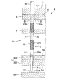
図2に示すように、検査側支持体5の対向壁面5Aから電極側支持体6の外壁面60までの距離L1は、荷重が加わっていない状態におけるプローブ3の全長より短く設定されている。この結果、支持部材10にプローブ3を支持させた際に、棒状体31の一端部31aは、支持部材10から一定の突出距離lbをもって突出した状態となる。
As shown in FIG. 2, the distance L1 from the facing
また、検査側支持体5の反対壁面5Bから電極側支持体6の外壁面60までの距離L2は、荷重が加わっていない状態における筒状体32の全長よりも短く設定されている。この結果、支持部材10にプローブ3を支持させた際に、筒状体32の他端部32bが、電極側支持体6の外壁面60から一定距離だけ突出した状態となる。
Further, the distance L2 from the
上述の構成を有する検査治具4を組み立てる際には、棒状体31の一端部31aを、プローブ支持孔61内から中間部支持孔71に挿入した後、検査側支持体5の支持孔51内に挿入する。これにより、筒状体32の他端部32b及び軸方向中間部近傍が、電極側支持体6及び中間部支持体7にそれぞれ支持される。また、棒状体31の一端部31aが、検査側支持体5に支持される。
When assembling the
次いで、電極板9と検査治具4との水平方向における位置決めを行った後、図7に示すように、電極板9を電極側支持体6の外壁面60に当接させて接合することにより、筒状体32のばね部32cを圧縮させて弾性変形させる。この結果、筒状体32の他端部32bが所定の押圧力で電極91に圧接されて、互いに導通接続される。
Next, after positioning the
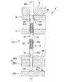
上述の検査治具4を用いて検査対象100の検査を行うには、検査対象100と検査治具4との水平方向における位置決めを行った後、図略の駆動機構により、検査治具4を昇降駆動する。そして、図8に示すように、プローブ3の一端部、具体的には棒状体31の一端部31aが、検査対象100の被検査部101に圧接されて、互いに導通接続される。また、筒状体32のばね部32cが、図7に示す状態から、さらに圧縮されて弾性変形することにより、棒状体31の一端部31aが、十分な押圧力で被検査部101に圧接される。
In order to inspect the
このようにして、棒状体31の一端部31aからなるプローブ3の一端部が、検査対象100の被検査部101に導通接続され、かつ筒状体32の他端部32bからなるプローブ3の後端部が、電極91に導通接続される。この状態で、プローブ3の後端部に電気信号が与えられることにより、検査対象100の検査が行われる。
In this manner, one end of the
本発明の第一実施形態に係る検査治具4は、図4に示すように、検査対象100への対向配置が予定されている第一支持体、具体的には検査対象100に対向した対向壁面5Aと、その反対側に位置する反対壁面5Bと有する検査側支持体5を備えている。この検査側支持体5には、対向壁面5Aから検査側支持体5の板厚方向中間部5C側に近づくにしたがって拡径する第一テーパ孔部53と、反対壁面5B側から検査側支持体5の板厚方向中間部5C側に近づくにしたがって拡径する第二テーパ孔部54とが設けられている。
The
また、検査側支持体5の反対壁面5B側に位置する支持孔51の上端開口部56の直径D2が、棒状体31の外径d1よりも大きく、かつ筒状体32の外径d2よりも小さい値に設定されている(図4参照)。さらに、検査側支持体5の対向壁面5A側に位置する支持孔51の下端開口部55の直径D1が、棒状体31の外径d1よりもやや大きい値とされている。
Further, the diameter D2 of the upper end opening 56 of the
したがって、棒状体31の一端部31aを、上端開口部56から支持孔51内に挿入して、検査側支持体5に支持させる際に、支持孔51の下端開口部55等により棒状体31の一端部31aが適正に拘束される。これにより、プローブ3の一端部と検査対象100の被検査部101とを正確に位置合わせすることが可能となる。
Therefore, when the one
プローブ3の棒状体31は、その外径d2が例えば30μm程度の極めて小さい値に形成されている。また、検査側支持体5の板厚Tは、検査側支持体5に圧接される筒状体32に一端部32aを安定して支持し得るように大きな値に設定されている。このため、検査側支持体5の板厚Tが、例えば棒状体31の外径d2の30倍以上に設定されている場合には、細径のドリルを使用して検査側支持体5に所定長さの孔加工を一度で施そうとすると、ドリルに折れ曲り等が生じ易い。
The rod-shaped
なお、ドリルの折れ曲り等を防止するために孔径を大きくすることも考えられるが、この場合には、プローブ3の一端部を安定して支持することが困難である。したがって、プローブ3のぐらつきが生じ易く、プローブ3の一端部と検査対象100の被検査部101との正確な位置合わせが困難となる。
It is possible to increase the hole diameter to prevent bending of the drill, but in this case, it is difficult to stably support one end of the
一方、図9に示す第一参考例では、支持体5を構成する下方の支持板521及び上方の支持板522にそれぞれストレート孔からなる下部ドリル孔511及び上部ドリル孔512がそれぞれ別々に設けられている。この構成によれば、支持体5の板厚Tが大きい場合であっても、ドリルDRの折れ曲がり等を防止しつつ、細径の下部ドリル孔511及び上部ドリル孔512を形成することが可能である。
On the other hand, in the first reference example shown in FIG. 9, the
しかし、図9に示すように構成した場合には、下方の支持板521に形成された下部ドリル孔511と、上方の支持板522に形成された上部ドリル孔512との間に位置ずれが生じ易い。このため、図9に示す第一参考例では、プローブの一端部を下部ドリル孔511及び上部ドリル孔512内に挿入する際に、上述の位置ずれ部において引っ掛かりが生じたり、プローブの摺動不良が生じたりし易かった。
However, in the case of the configuration shown in FIG. 9, there is a displacement between the
これに対して本発明の第一実施形態では、図4に示すように、対向壁面5A側から板厚方向中間部5C側に近づくにしたがって拡径する第一テーパ孔部53と、反対壁面5B側から板厚方向中間部5C側に近づくにしたがって拡径する第二テーパ孔部54とを検査側支持体5に設けている。この結果、板厚方向中間部5Cに位置する棒状体支持孔の直径D3は、対向壁面5Aに位置する下端開口部55の直径D1及び反対壁面5Bに位置する上端開口部56の直径D2よりも大きな値に形成される。
On the other hand, in the first embodiment of the present invention, as shown in FIG. 4, the first
したがって、第一テーパ孔部53が形成された第一支持板501と、第二テーパ孔部54が形成された第二支持板502とを重ね合わせる際に、第一テーパ孔部53と第二テーパ孔部54との間に多少の位置ずれが生じた場合でも、この位置ずれ部においてプローブ3の引っ掛かり等が生じにくい。このため、棒状体31の一端部31aを、第二テーパ孔部54から第一テーパ孔部53へとスムーズに挿入することが可能である。
Therefore, when the
しかも、対向壁面5Aに位置ずる下端開口部55の直径D1が、板厚方向中間部5Cに位置する支持孔51の直径D3よりも小さな値に形成されるため、棒状体31の一端部31aからなるプローブ3の一端部を、下端開口部55により適正に拘束して、プローブ3のぐらつきを効果的に防止することができる。
In addition, since the diameter D1 of the
さらに、プローブの引っ掛かりを防止するため、図10に示す第二参考例のように、大径の中間部ドリル孔513及び小径の下部ドリル孔511を下方の支持板521に設けるとともに、小径の上部ドリル孔512を支持板522に設ける構成を採用した場合には、三回のドリル孔加工が必要となる。これに対して、本発明の第一実施形態に係る検査治具4では、ドリル等を使用した孔加工の回数を減らすことが可能である。このため、検査治具4の生産性を効果的に向上させることができる。
Further, in order to prevent the probe from being caught, as in the second reference example shown in FIG. 10, a large-diameter middle
上述の第一実施形態では、図4等に示すように、プローブ3が、導電性部材からなる棒状体31と、この棒状体31に外嵌される導電性部材からなる筒状体32とを有し、かつ筒状体32に、螺旋状のばね部32cが設けられた構成としている。そして、対向壁面5A側に位置する支持孔51の下端開口部55の直径D3を、棒状体31の外径d1よりもやや大きい値とすることにより、棒状体31一端部31aを、下端開口部55により拘束している。これにより、プローブ3の一端部と、検査対象100の被検査部101とを正確に位置合わせすることができる。
In the above-described first embodiment, as shown in FIG. 4 and the like, the
また、反対壁面5B側に位置する上端開口部56の直径D2が、筒状体32の外径d2よりも小さい値に設定されているので、筒状体32の一端部32aが、検査側支持体5の反対壁面5Bに圧接されて係止される。その結果、検査側支持体5には、筒状体32から大きな圧接力が作用する。しかしながら、上述のように検査側支持体5の板厚Tを、十分な強度が得られる厚さに設定することができるため、筒状体32の一端部32aを安定して支持することができる。
Further, since the diameter D2 of the upper end opening 56 located on the
なお、上述の第一実施形態では、検査対象100への対向配置が予定されている検査側支持体5からなる第一支持体に、第一テーパ孔部53及び第二テーパ孔部54を備えた支持孔51を形成した例について説明した。これに限られず、プローブ3を支持する他の支持体、例えば電極側支持体6又は中間部支持体7からなる第二支持体に、その一壁面側から板厚方向中間部側に近づくにしたがって拡径する第一テーパ孔部等を設けた構成としてもよい。
In the above-described first embodiment, the first support body including the inspection-
また、導電性部材からなる棒状体31と、この棒状体31が挿入される導電性部材からなる筒状体32とを有するプローブ3を備えた上述の第一実施形態に代え、導電性部材により所定長さの針状に形成されたニードルタイプのプローブを備えた検査治具4、及びこの検査治具4を備えた検査装置1についても本発明を適用可能である。
Further, instead of the above-described first embodiment including the
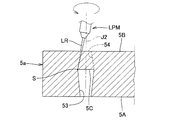
なお、図12に示す第一実施形態の変形例に係る検査治具41は、一枚の板材からなる検査側支持体5aを備えている。そして、検査側支持体5aの対向壁面5A側部分に第一テーパ孔部53が設けられるとともに、反対壁面5B側部分に第二テーパ孔部54が設けられている。
The
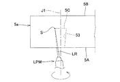
第一テーパ孔部53を形成するには、図13に示すように、対向壁面5Aの下方側にレーザ加工機LPMを配置し、レーザ加工機LPMから照射されるレーザ光LRの照射方向を、第一テーパ孔部53の周壁面に沿わせる。また、レーザ光LRの焦点Sを、検査側支持体5の板厚方向中間部5Cに合わせるようにセットする。
In order to form the first
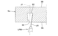
そして、レーザ加工機LPMから検査側支持体5aの対向壁面5Aに向けてレーザ光LRを照射しつつ、第一テーパ孔部53の軸心J1を中心に、レーザ加工機LPMを一回転以上、旋回させる。これにより、図14に示すように、対向壁面5A側から検査側支持体5aの板厚方向中間部5C側に至るにしたがって拡径する第一テーパ孔部53が形成される。
Then, while irradiating the laser beam LR from the laser processing machine LPM toward the facing
次いで、図15に示すように、反対壁面5Bの上方側にレーザ加工機LPMを配置し、レーザ加工機LPMから照射されるレーザ光LRの照射方向を、第二テーパ孔部54の周壁面に沿わせる。また、レーザ光LRの焦点Sを、検査側支持体5aの板厚方向中間部5Cに合わせるようにセットする。
Next, as shown in FIG. 15, the laser processing machine LPM is arranged above the
そして、第一テーパ孔部53の形成方法と同様にして、レーザ加工機LPMからレーザ光LRを、検査側支持体5aの反対壁面5Bに向けて照射つつ、第二テーパ孔部54の軸心J2を中心に、レーザ加工機LPMを旋回させる。これにより、図12に示すように、反対壁面5B側から検査側支持体5aの板厚方向中間部5C側に至るにしたがって拡径する第二テーパ孔部54が形成される。
Then, similarly to the method of forming the first
なお、上述の第一実施形態では、図4及び図11等に示すように、第一支持板501及び第二支持板502に、第一テーパ孔部53及び第二テーパ孔部54をそれぞれ個別に形成している。このため、第一支持板501及び第二支持板502を位置合わせして重ね合わせる際に、位置合わせ誤差が生じる可能性があった。これに対して、図12に示す変形例の検査治具41では、一枚の板材からなる検査側支持体5aに、第一テーパ孔部53a及び第二テーパ孔部54aの両方が設けられているため、第一テーパ孔部53aの軸心J1と第二テーパ孔部54aの軸心J2とのずれを、効果的に小さくすることができる。
In the above-described first embodiment, as shown in FIGS. 4 and 11, etc., the first
また、3Dプリンタを用いて上述の検査側支持体5aを形成してもよい。この場合、第一テーパ孔部53及び第二テーパ孔部54を検査側支持体5aに連続して形成することができる。
Further, the
なお、第一テーパ孔部53及び第二テーパ孔部54の両方を検査側支持体5,5aに形成してなる上述の第一実施形態に代え、後述の第二実施形態及び第三実施形態に示すように、対向壁面5A又は反対壁面5Bの何れか一方側にのみ、第一テーパ孔部53を設けた構成としてもよい。
(第二実施形態)
It should be noted that instead of the above-described first embodiment in which both the first
(Second embodiment)
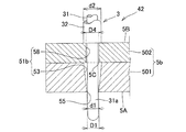
図16は、本発明に係る検査治具42の第二実施形態を示している。この検査治具42は、対向壁面5A側から検査側支持体5bの板厚方向中間部5C側に近づくにしたがって拡径する第一テーパ孔部53と、反対壁面5B側から検査側支持体5bの板厚方向中間部5C側に均一な口径D4で延びるストレート孔部58とを備えている。そして、第一テーパ孔部53及びストレート孔部58により、棒状体31の一端部31aを支持する支持孔51bが構成されている。
FIG. 16 shows a second embodiment of the
検査側支持体5bの対向壁面A側に位置する第一テーパ孔部53の直径D1は、棒状体31の外径d1よりもやや大きい値とされている。また、検査側支持体5bの反対壁面B側に位置するストレート孔部58の口径D4は、棒状体31の外径d1よりもやや大きく、かつプローブ3の筒状体32の外径d2よりも小さい値とされている。
The diameter D1 of the first
この構成においても、第一支持板501及び第二支持板502からなる検査側支持体5bの板厚を十分な値に設定することにより、検査側支持体5bの反対壁面5Bにおいてプローブ3の筒状体32を安定して支持することができる。そして、対向壁面5A側の第一テーパ孔部53と、反対壁面5Bのストレート孔部58との間に位置ずれが生じた場合においても、棒状体31の一端部31aをストレート孔部58から第一テーパ孔部53へと挿入する際に、上述の位置ずれ部において引っ掛かり等が生じにくいという利点がある。
Also in this configuration, by setting the plate thickness of the
しかも、対向壁面5A側に位置する第一テーパ孔部53の下端部の直径D1が、板厚方向中間部5C側に位置する第一テーパ孔部53の上端部に比べて小さくなっている。このため、棒状体31の一端部31aが、第一テーパ孔部53の下端開口部55により効果的に拘束されて、プローブ3のぐらつきが抑制される。したがって、プローブ3の一端部と検査対象の被検査部とを正確に位置合わせすることができる。
Moreover, the diameter D1 of the lower end portion of the first
上述の第二実施形態においても、図4等に示す第一実施形態に係る検査治具4と同様に、検査側支持体5bが、対向壁面5A側に位置する第一支持板501と、反対壁面5B側に位置する第二支持板502とを有する構成としている。この構成によれば、テーパリーマ又はレーザ加工機等を利用して、第一支持板501に第一テーパ孔部53を容易に形成できる。また、ストレートドリル又はレーザ加工機等を使用して、第二支持板502にストレート孔部58を容易に形成できるという利点がある。
Also in the above-described second embodiment, the inspection-
なお、本発明の第二実施形態に係る検査治具42においても、3Dプリンタにより一枚板からなる検査側支持体5を形成してもよい。この場合には、検査側支持体5を3Dプリンタにより形成する際に、第一テーパ孔部53及びストレート孔部58を連続して形成することができる。
(第三実施形態)
In addition, also in the
(Third embodiment)
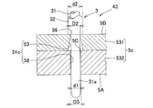
図17は、本発明の第三実施形態に係る検査治具43を示している。この検査治具43は、反対壁面5B側に配設された第一支持板531と、対向壁面5A側に配設された第二支持板532とにより検査側支持体5cが構成されている。
FIG. 17 shows an
そして、第一支持板531には、反対壁面5Bから検査側支持体5cの板厚方向中間部5C側に近づくにしたがって拡径する第一テーパ孔部53が形成されている。また、第二支持板532には、対向壁面5A側から検査側支持体5cの板厚方向中間部5C側に均一な口径で延びるストレート孔部58が形成されている。そして、第一テーパ孔部53及びストレート孔部58により、棒状体31の一端部31aを支持する支持孔51cが形成されている。また、ストレート孔部58の口径D5は、棒状体31の外径d1よりも大きい値とされている。
Then, the
この構成においても、検査側支持体5cの板厚を十分な値に設定して、この検査側支持体5cによりプローブ3の筒状体32を安定して支持することができる。そして、ストレート孔部58の口径D5が、棒状体31の外径d1よりも十分に大きい値としている。これにより、第一テーパ孔部53とストレート孔部58との間に軸心の位置ずれが生じた場合でも、この位置ずれ部において引っ掛かり等を生じることなく、棒状体31の一端部31aを第一テーパ孔部53からストレート孔部58へとスムーズに挿入することができる。
Also in this configuration, the plate thickness of the
しかも、検査側支持体5cの反対壁面5B側に位置する第一テーパ孔部53の上端開口部56の直径D2が、検査側支持体5cの板厚方向中間部5C側に位置する第一テーパ孔部53の下端部に比べて小さく形成される。このため、棒状体31の一端部31aが、第一テーパ孔部53の上端開口部56により拘束されて、プローブ3のぐらつきが防止される。したがって、プローブ3の一端部と検査対象の被検査部とを正確に位置合わせすることができる。
Moreover, the diameter D2 of the upper end opening 56 of the first
また、上述の第三実施形態では、検査側支持体5cが、反対壁面5B側に位置する第一支持板531と、対向壁面5A側に位置する第二支持板532とを有する構成としている。この構成によれば、テーパリーマ又はレーザ加工機等を使用して、第一支持板531に第一テーパ孔部53を容易に形成できる。また、ストレートドリル又はレーザ加工機等を使用して、第二支持板532にストレート孔部58を容易に形成できるという利点がある。
In addition, in the third embodiment described above, the inspection
上述の第三実施形態に係る検査治具43においても、3Dプリンタにより一枚板からなる検査側支持体5を形成することが可能である。
Also in the
上述のように本発明の一例に係る検査治具は、一端部が検査対象に圧接される棒状のプローブと、前記プローブを支持する支持孔を有する板状の第一支持体とを備え、前記支持孔は、前記第一支持体の一壁面側から前記第一支持体の板厚方向中間部側に近づくにしたがって拡径する第一テーパ孔部を備えている。 As described above, the inspection jig according to the example of the present invention includes a rod-shaped probe whose one end is pressed against an inspection target, and a plate-shaped first support having a support hole for supporting the probe, The support hole includes a first taper hole portion whose diameter increases from one wall surface side of the first support member toward the intermediate portion side in the plate thickness direction of the first support member.
この構成によれば、第一支持体の板厚が大きい場合においても、煩雑な孔加工作業を要することなく、プローブを安定して支持することができる。このため、プローブと検査対象の被検査部等とを正確に位置合わせすることが可能な検査治具を効率よく生産することができる。 According to this configuration, even when the plate thickness of the first support is large, the probe can be stably supported without requiring a complicated hole forming operation. Therefore, it is possible to efficiently produce an inspection jig capable of accurately aligning the probe and the inspected portion to be inspected.
また、前記支持孔は、前記一壁面側の反対側に位置する他壁面側から前記板厚方向中間部側に近づくにしたがって拡径する第二テーパ孔部を、さらに備えた構成とすることが好ましい。 In addition, the support hole may further include a second taper hole portion whose diameter increases from the other wall surface side opposite to the one wall surface side toward the plate thickness direction intermediate portion side. preferable.
この構成によれば、一壁面側の第一テーパ孔部と、他壁面側の第二テーパ孔部とを別々に形成する際に、両者の間に多少の位置ずれが生じた場合でも、プローブの一端部を第二テーパ孔部から第一テーパ孔部へと挿入する際に、上述の位置ずれ部において引っ掛かりが生じること等を効果的に防止できる。しかも、一壁面側に位置する第一テーパ孔部の開口部により、プローブを拘束して、そのぐらつきを防止できるため、プローブと、検査対象の被検査部等とを正確に位置合わせすることが可能である。 According to this structure, when the first taper hole portion on the one wall surface side and the second taper hole portion on the other wall surface side are separately formed, even if a slight misalignment occurs between them, the probe It is possible to effectively prevent the above-mentioned misalignment from being caught when the one end of the is inserted into the first taper hole from the second taper hole. Moreover, since the probe can be restrained and the wobble can be prevented by the opening portion of the first tapered hole portion located on the one wall surface side, the probe and the inspected portion to be inspected can be accurately aligned. It is possible.
また、前記支持孔は、前記一壁面側の反対側に位置する他壁面側から前記板厚方向中間部側に均一な口径で延びるストレート孔部を、さらに備えた構成としてもよい。 In addition, the support hole may further include a straight hole portion extending from the other wall surface side opposite to the one wall surface side to the intermediate portion side in the plate thickness direction with a uniform diameter.
この構成によれば、第一支持体の板厚を十分な値に設定することにより、プローブを安定して支持することができる。そして、上述のテーパ孔部とストレート孔部との間に位置ずれが生じ場合においても、この位置ずれ部において引っ掛かり等を生じることなく、プローブを支持孔内へスムーズに挿入することができる。しかも、第一支持体の一壁面側に位置する第一テーパ孔部の開口部により、プローブを拘束して、そのぐらつきを防止できるため、プローブと検査対象の被検査部とを正確に位置合わせすることができる。 According to this configuration, the probe can be stably supported by setting the plate thickness of the first support to a sufficient value. Then, even if a displacement occurs between the tapered hole portion and the straight hole portion, the probe can be smoothly inserted into the support hole without being caught at the displacement portion. Moreover, since the probe can be restrained by the opening of the first tapered hole located on the one wall surface side of the first support and the wobble can be prevented, the probe and the inspected part to be inspected can be accurately aligned. can do.
また、前記第一支持体は、前記一壁面側に位置する第一支持板と、前記他壁面側に位置する第二支持板とを有し、前記第一テーパ孔部が、前記第一支持板に設けられた構成としてもよい。 The first support has a first support plate located on the one wall surface side and a second support plate located on the other wall surface side, and the first tapered hole portion is the first support plate. It may be configured to be provided on the plate.
この構成によれば、テーパリーマ等を使用して、第一支持板に第一テーパ孔部を容易に形成することができる。そして、第一支持板と第二支持板とを重ね合わせて接合することにより、第一テーパ孔部を備えた支持孔が第一支持体に設けられることになる。 According to this configuration, the first tapered hole portion can be easily formed in the first support plate by using the taper reamer or the like. Then, by overlapping and joining the first support plate and the second support plate, the support hole having the first tapered hole portion is provided in the first support body.
また、前記検査治具は、前記プローブを支持する第二支持体を、さらに備え、前記第一支持体は、前記検査対象への対向配置が予定されていることが好ましい。 Further, it is preferable that the inspection jig further includes a second support body that supports the probe, and the first support body is planned to be arranged to face the inspection target.
この構成によれば、第一の板厚が大きい場合においても、煩雑な孔加工作業を要することなく、検査対象に近接したプローブの一端部を支持体により安定して支持することができる。このため、プローブの一端部と検査対象の被検査部とを正確に位置合わせすることができる。 According to this configuration, even when the first plate thickness is large, one end of the probe close to the inspection target can be stably supported by the support without requiring a complicated hole machining operation. Therefore, the one end of the probe and the inspected portion to be inspected can be accurately aligned.
また、前記プローブは、前記支持孔に一端部が支持される導電性部材からなる棒状体と、前記棒状体に外嵌される導電性部材からなる筒状体とを有し、前記筒状体には、螺旋状のばね部が設けられ、前記一壁面側に位置する前記第一テーパ孔部の直径は、前記棒状体の外径よりも大きく、前記筒状体の外径より小さいことが好ましい。 The probe has a rod-shaped body made of a conductive member whose one end is supported in the support hole, and a tubular body made of a conductive member fitted on the rod-shaped body. Is provided with a spiral spring portion, and the diameter of the first tapered hole portion located on the one wall surface side is larger than the outer diameter of the rod-shaped body and smaller than the outer diameter of the cylindrical body. preferable.
この構成によれば、一壁面側に位置する第一テーパ孔部の開口部により、プローブの棒状体を拘束して、そのぐらつきを防止できるため、棒状体の一端部と、検査対象の被検査部とを正確に位置合わせすることが可能である。 According to this configuration, the opening of the first tapered hole located on the one wall surface can restrain the rod-shaped body of the probe and prevent its wobbling. Therefore, one end of the rod-shaped body and the object to be inspected It is possible to align the parts accurately.
本発明の一例に係る検査治具の製造方法は、前記第一支持板に前記第一テーパ孔部を形成する第一テーパ孔部形成工程と、前記第一支持板と前記第二支持板とを重ね合わせて接合する接合工程とを含むものである。 A method for manufacturing an inspection jig according to an example of the present invention includes a first tapered hole forming step of forming the first tapered hole in the first supporting plate, the first supporting plate and the second supporting plate. And a joining step of joining them by superposing.
この構成によれば、テーパリーマ等を使用して、第一支持板に第一テーパ孔部を容易に形成することができる。そして、第一支持板と第二支持板とを重ね合わせて接合することにより、第一テーパ孔部を備えた支持孔が支持体に設けられる。 According to this structure, the first tapered hole portion can be easily formed in the first support plate by using the taper reamer or the like. Then, the first support plate and the second support plate are overlapped and bonded to each other, whereby the support hole having the first tapered hole portion is provided in the support body.
また、前記テーパ孔部形成工程は、前記一壁面側にレーザ加工機を配置し、前記レーザ加工機から照射されるレーザ光の照射方向を前記第一テーパ孔部の周壁面に沿わせるようにセットした後、前記レーザ加工機から前記第一支持板にレーザ光を照射しつつ、前記第一テーパ孔部の軸心を中心に、前記レーザ加工機を旋回させることにより、前記第一テーパ孔部を形成することが好ましい。 Further, in the taper hole forming step, a laser processing machine is arranged on the one wall surface side so that the irradiation direction of the laser light emitted from the laser processing machine is along the peripheral wall surface of the first taper hole portion. After setting, while irradiating the first supporting plate with laser light from the laser processing machine, the laser processing machine is turned about the axis of the first taper hole portion, whereby the first taper hole is formed. It is preferable to form a part.
この構成によれば、レーザ加工機を使用して、第一支持板に第一テーパ孔部を容易かつ適正に形成することができる。 With this configuration, the first taper hole portion can be easily and properly formed in the first support plate by using the laser processing machine.
また、本発明の一例に係る検査装置は、前記検査治具と、前記プローブの後端部に対して電気的に接続されるとともに、前記プローブの後端部に電気信号を与えて検査対象の検査を行う検査部とを備えている。 In addition, the inspection device according to an example of the present invention is electrically connected to the inspection jig and the rear end portion of the probe, and applies an electric signal to the rear end portion of the probe to inspect an object to be inspected. An inspection unit for performing inspection is provided.
この構成によれば、第一支持体の板厚が大きい場合においても、煩雑な加工作業を要することなく、プローブを安定して支持することにより、プローブの一端部と検査対象の被検査部とを正確に位置合わせした状態で、検査対象の検査を適正に行うことができる。 According to this configuration, even when the plate thickness of the first support is large, by stably supporting the probe without requiring complicated processing work, one end of the probe and the inspected part to be inspected are The inspection of the inspection object can be properly performed in the state where the is accurately aligned.
1 検査装置
3 プローブ
4,4U,4L,41,42,43 検査治具
5,5a,5b,5c 検査側支持体(第一支持体)
5A 対向壁面
5B 反対壁面
5C 板厚方向中間部
6 電極側支持体(第二支持体)
7 中間部支持体(第二支持体)
9 電極板
10 支持部材
11 筐体
12 検査対象固定装置
13 第一検査部
14 第二検査部
15 検査部移動機構
20 制御部
31 棒状体
31a 棒状体の一端部
31b 棒状体の他端部
31c 棒状体の先端接触部
32 筒状体
32a 筒状体の一端部
32b 筒状体の他端部
32c ばね部
51,51b,51c 支持孔
53 第一テーパ孔部
54 第二テーパ孔部
55 下端開口部
56 上端開口部
57 隔離壁
58 ストレート孔部
60 支持部材の外壁面
61 プローブ支持孔
71 中間部支持孔
90 導電線
91 電極
100 検査対象
101 被検査部
501,531 第一支持板
502,532 第二支持板
d1 棒状体の外径
D1 開口部の直径
d2 筒状体の外径
D2 開口部の直径
D3 板厚方向中間部の直径
D4 ストレート孔部の口径
D5 ストレート孔部の口径
DR ドリル
J1,J2 軸心
la 棒状体の突出長さ
lb 棒状体の突出距離
LPM レーザ加工機
LR レーザ光
P 棒状体支持孔の配列ピッチ
S レーザ光の焦点
T 検査側支持体の板厚
1
5A
7 Intermediate part support (second support)
Claims (9)
前記プローブを支持する支持孔を有する板状の第一支持体とを備え、
前記支持孔は、前記第一支持体の一壁面側から前記第一支持体の板厚方向中間部側に近づくにしたがって拡径する第一テーパ孔部を備えている検査治具。 A rod-shaped probe whose one end is pressed against the inspection target,
A plate-shaped first support having a support hole for supporting the probe,
The said support hole is an inspection jig provided with the 1st taper hole part which diameter-expands as approaching the board thickness direction intermediate part side of the said 1st support body from the one wall surface side of the said 1st support body.
前記第一テーパ孔部が、前記第一支持板に設けられている請求項2又は3に記載の検査治具。 The first support has a first support plate located on the one wall surface side and a second support plate located on the other wall surface side,
The inspection jig according to claim 2 or 3, wherein the first tapered hole portion is provided in the first support plate.
前記第一支持体は、前記検査対象への対向配置が予定されている請求項1〜4の何れか1項に記載の検査治具。 The inspection jig further includes a second support body that supports the probe,
The inspection jig according to any one of claims 1 to 4, wherein the first support is planned to be arranged to face the inspection target.
前記筒状体には、螺旋状のばね部が設けられ、
前記一壁面側に位置する前記第一テーパ孔部の直径は、前記棒状体の外径よりも大きく、前記筒状体の外径より小さい請求項5に記載の検査治具。 The probe has a rod-shaped body made of a conductive member, and a cylindrical body made of a conductive member into which the rod-shaped body is inserted,
The cylindrical body is provided with a spiral spring portion,
The inspection jig according to claim 5, wherein a diameter of the first tapered hole portion located on the one wall surface side is larger than an outer diameter of the rod-shaped body and smaller than an outer diameter of the cylindrical body.
前記第一支持板に前記第一テーパ孔部を形成する第一テーパ孔部形成工程と、
前記第一支持板と前記第二支持板とを重ね合わせて接合する接合工程とを含む検査治具の製造方法。 The method for manufacturing an inspection jig according to claim 4,
A first tapered hole portion forming step of forming the first tapered hole portion on the first support plate;
A method for manufacturing an inspection jig, comprising: a joining step of joining the first support plate and the second support plate in an overlapping manner.
The inspection jig according to any one of claims 1 to 6 is electrically connected to a rear end portion of the probe, and an electric signal is applied to the rear end portion of the probe to inspect the inspection target. An inspection device including an inspection unit that performs an inspection.
Priority Applications (4)
| Application Number | Priority Date | Filing Date | Title |
|---|---|---|---|
| JP2018239188A JP2020101427A (en) | 2018-12-21 | 2018-12-21 | Inspection jig, manufacturing method of inspection jig, and inspection device including inspection jig |
| US16/716,500 US20200200797A1 (en) | 2018-12-21 | 2019-12-17 | Inspection jig, method for manufacturing inspection jig, and inspection apparatus including inspection jig |
| CN201911298847.1A CN111352018A (en) | 2018-12-21 | 2019-12-17 | Inspection jig, method of manufacturing the same, and inspection apparatus having the same |
| TW108146541A TW202024648A (en) | 2018-12-21 | 2019-12-19 | Inspection jig, method for manufacturing inspection jig, and inspection apparatus including inspection jig |
Applications Claiming Priority (1)
| Application Number | Priority Date | Filing Date | Title |
|---|---|---|---|
| JP2018239188A JP2020101427A (en) | 2018-12-21 | 2018-12-21 | Inspection jig, manufacturing method of inspection jig, and inspection device including inspection jig |
Publications (1)
| Publication Number | Publication Date |
|---|---|
| JP2020101427A true JP2020101427A (en) | 2020-07-02 |
Family
ID=71098384
Family Applications (1)
| Application Number | Title | Priority Date | Filing Date |
|---|---|---|---|
| JP2018239188A Pending JP2020101427A (en) | 2018-12-21 | 2018-12-21 | Inspection jig, manufacturing method of inspection jig, and inspection device including inspection jig |
Country Status (4)
| Country | Link |
|---|---|
| US (1) | US20200200797A1 (en) |
| JP (1) | JP2020101427A (en) |
| CN (1) | CN111352018A (en) |
| TW (1) | TW202024648A (en) |
Families Citing this family (1)
| Publication number | Priority date | Publication date | Assignee | Title |
|---|---|---|---|---|
| CN116214914B (en) * | 2022-12-15 | 2026-02-13 | 深圳光韵达光电科技股份有限公司 | A method for 3D printing probe molds |
Citations (6)
| Publication number | Priority date | Publication date | Assignee | Title |
|---|---|---|---|---|
| JPH08201427A (en) * | 1995-01-20 | 1996-08-09 | Hitachi Ltd | A probe assembly and a positioning board in which a plurality of probes are positioned and arranged |
| WO2004072661A1 (en) * | 2003-02-17 | 2004-08-26 | Kabushiki Kaisha Nihon Micronics | Electrical connection device |
| JP2007024664A (en) * | 2005-07-15 | 2007-02-01 | Japan Electronic Materials Corp | Vertical coil spring probe and probe unit using the same |
| US20080048685A1 (en) * | 2006-08-28 | 2008-02-28 | Corad Technology Inc. | Probe card having vertical probes |
| JP5822042B1 (en) * | 2015-03-27 | 2015-11-24 | 日本電産リード株式会社 | Inspection jig, substrate inspection apparatus, and manufacturing method of inspection jig |
| JP2017054773A (en) * | 2015-09-11 | 2017-03-16 | 日本電産リード株式会社 | Connection jig, substrate inspection device, and manufacturing method for connection jig |
Family Cites Families (3)
| Publication number | Priority date | Publication date | Assignee | Title |
|---|---|---|---|---|
| TWI554763B (en) * | 2015-10-28 | 2016-10-21 | 旺矽科技股份有限公司 | Probe head |
| CN109564244B (en) * | 2016-07-28 | 2022-01-07 | 日本电产理德股份有限公司 | Inspection aid, substrate inspection device, and method for manufacturing inspection aid |
| WO2018198859A1 (en) * | 2017-04-27 | 2018-11-01 | 日本電産リード株式会社 | Inspection jig, and substrate inspecting device |
-
2018
- 2018-12-21 JP JP2018239188A patent/JP2020101427A/en active Pending
-
2019
- 2019-12-17 US US16/716,500 patent/US20200200797A1/en not_active Abandoned
- 2019-12-17 CN CN201911298847.1A patent/CN111352018A/en not_active Withdrawn
- 2019-12-19 TW TW108146541A patent/TW202024648A/en unknown
Patent Citations (6)
| Publication number | Priority date | Publication date | Assignee | Title |
|---|---|---|---|---|
| JPH08201427A (en) * | 1995-01-20 | 1996-08-09 | Hitachi Ltd | A probe assembly and a positioning board in which a plurality of probes are positioned and arranged |
| WO2004072661A1 (en) * | 2003-02-17 | 2004-08-26 | Kabushiki Kaisha Nihon Micronics | Electrical connection device |
| JP2007024664A (en) * | 2005-07-15 | 2007-02-01 | Japan Electronic Materials Corp | Vertical coil spring probe and probe unit using the same |
| US20080048685A1 (en) * | 2006-08-28 | 2008-02-28 | Corad Technology Inc. | Probe card having vertical probes |
| JP5822042B1 (en) * | 2015-03-27 | 2015-11-24 | 日本電産リード株式会社 | Inspection jig, substrate inspection apparatus, and manufacturing method of inspection jig |
| JP2017054773A (en) * | 2015-09-11 | 2017-03-16 | 日本電産リード株式会社 | Connection jig, substrate inspection device, and manufacturing method for connection jig |
Also Published As
| Publication number | Publication date |
|---|---|
| US20200200797A1 (en) | 2020-06-25 |
| CN111352018A (en) | 2020-06-30 |
| TW202024648A (en) | 2020-07-01 |
Similar Documents
| Publication | Publication Date | Title |
|---|---|---|
| TWI789922B (en) | Inspection jig, and inspection apparatus | |
| TWI821332B (en) | Inspection jig, and inspection apparatus | |
| JP3394620B2 (en) | Probe assembly and inspection device | |
| WO2017138305A1 (en) | Contact terminal, inspection jig, and inspection device | |
| JP2019015542A (en) | Contact terminal, inspection jig, and inspection device | |
| TW202014711A (en) | Inspection jig, inspection device, and contact terminal | |
| KR20210111774A (en) | Contact terminals, inspection jigs and inspection devices | |
| JP2017054773A (en) | Connection jig, substrate inspection device, and manufacturing method for connection jig | |
| JP6613844B2 (en) | Inspection jig, substrate inspection apparatus, and substrate inspection method | |
| CN111352018A (en) | Inspection jig, method of manufacturing the same, and inspection apparatus having the same | |
| US11327094B2 (en) | Inspection jig, and inspection device including the same | |
| JP7605203B2 (en) | Contact terminal, inspection tool, and inspection device | |
| JP5217063B2 (en) | Inspection method and inspection apparatus | |
| JP4326495B2 (en) | Method for assembling semiconductor substrate inspection apparatus | |
| WO2021039898A1 (en) | Inspection jig and inspection device | |
| CN112986636B (en) | Positionable probe card and manufacturing method thereof | |
| JP2010185784A (en) | Substrate inspection apparatus and method of aligning the same | |
| JP2007053207A (en) | Component mounting state inspection apparatus and method | |
| KR101097157B1 (en) | Probe card | |
| KR101097156B1 (en) | Joining method of metal rod of auxiliary board for probe card |
Legal Events
| Date | Code | Title | Description |
|---|---|---|---|
| A621 | Written request for application examination |
Free format text: JAPANESE INTERMEDIATE CODE: A621 Effective date: 20211118 |
|
| RD03 | Notification of appointment of power of attorney |
Free format text: JAPANESE INTERMEDIATE CODE: A7423 Effective date: 20211118 |
|
| RD04 | Notification of resignation of power of attorney |
Free format text: JAPANESE INTERMEDIATE CODE: A7424 Effective date: 20220401 |
|
| A977 | Report on retrieval |
Free format text: JAPANESE INTERMEDIATE CODE: A971007 Effective date: 20221027 |
|
| A131 | Notification of reasons for refusal |
Free format text: JAPANESE INTERMEDIATE CODE: A131 Effective date: 20221108 |
|
| A02 | Decision of refusal |
Free format text: JAPANESE INTERMEDIATE CODE: A02 Effective date: 20230425 |