JP2020143976A - 電気的接続装置 - Google Patents
電気的接続装置 Download PDFInfo
- Publication number
- JP2020143976A JP2020143976A JP2019040144A JP2019040144A JP2020143976A JP 2020143976 A JP2020143976 A JP 2020143976A JP 2019040144 A JP2019040144 A JP 2019040144A JP 2019040144 A JP2019040144 A JP 2019040144A JP 2020143976 A JP2020143976 A JP 2020143976A
- Authority
- JP
- Japan
- Prior art keywords
- probe
- guide plate
- connection device
- electrical connection
- region
- Prior art date
- Legal status (The legal status is an assumption and is not a legal conclusion. Google has not performed a legal analysis and makes no representation as to the accuracy of the status listed.)
- Granted
Links
Images






Classifications
-
- G—PHYSICS
- G01—MEASURING; TESTING
- G01R—MEASURING ELECTRIC VARIABLES; MEASURING MAGNETIC VARIABLES
- G01R1/00—Details of instruments or arrangements of the types included in groups G01R5/00 - G01R13/00 and G01R31/00
- G01R1/02—General constructional details
- G01R1/06—Measuring leads; Measuring probes
- G01R1/067—Measuring probes
- G01R1/073—Multiple probes
- G01R1/07307—Multiple probes with individual probe elements, e.g. needles, cantilever beams or bump contacts, fixed in relation to each other, e.g. bed of nails fixture or probe card
- G01R1/07314—Multiple probes with individual probe elements, e.g. needles, cantilever beams or bump contacts, fixed in relation to each other, e.g. bed of nails fixture or probe card the body of the probe being perpendicular to test object, e.g. bed of nails or probe with bump contacts on a rigid support
-
- G—PHYSICS
- G01—MEASURING; TESTING
- G01R—MEASURING ELECTRIC VARIABLES; MEASURING MAGNETIC VARIABLES
- G01R1/00—Details of instruments or arrangements of the types included in groups G01R5/00 - G01R13/00 and G01R31/00
- G01R1/02—General constructional details
- G01R1/06—Measuring leads; Measuring probes
- G01R1/067—Measuring probes
- G01R1/073—Multiple probes
- G01R1/07307—Multiple probes with individual probe elements, e.g. needles, cantilever beams or bump contacts, fixed in relation to each other, e.g. bed of nails fixture or probe card
- G01R1/07357—Multiple probes with individual probe elements, e.g. needles, cantilever beams or bump contacts, fixed in relation to each other, e.g. bed of nails fixture or probe card with flexible bodies, e.g. buckling beams
-
- G—PHYSICS
- G01—MEASURING; TESTING
- G01R—MEASURING ELECTRIC VARIABLES; MEASURING MAGNETIC VARIABLES
- G01R1/00—Details of instruments or arrangements of the types included in groups G01R5/00 - G01R13/00 and G01R31/00
- G01R1/02—General constructional details
- G01R1/06—Measuring leads; Measuring probes
- G01R1/067—Measuring probes
- G01R1/06711—Probe needles; Cantilever beams; "Bump" contacts; Replaceable probe pins
-
- G—PHYSICS
- G01—MEASURING; TESTING
- G01R—MEASURING ELECTRIC VARIABLES; MEASURING MAGNETIC VARIABLES
- G01R1/00—Details of instruments or arrangements of the types included in groups G01R5/00 - G01R13/00 and G01R31/00
- G01R1/02—General constructional details
- G01R1/06—Measuring leads; Measuring probes
- G01R1/067—Measuring probes
- G01R1/06711—Probe needles; Cantilever beams; "Bump" contacts; Replaceable probe pins
- G01R1/06733—Geometry aspects
-
- G—PHYSICS
- G01—MEASURING; TESTING
- G01R—MEASURING ELECTRIC VARIABLES; MEASURING MAGNETIC VARIABLES
- G01R1/00—Details of instruments or arrangements of the types included in groups G01R5/00 - G01R13/00 and G01R31/00
- G01R1/02—General constructional details
- G01R1/06—Measuring leads; Measuring probes
- G01R1/067—Measuring probes
- G01R1/06711—Probe needles; Cantilever beams; "Bump" contacts; Replaceable probe pins
- G01R1/06755—Material aspects
-
- G—PHYSICS
- G01—MEASURING; TESTING
- G01R—MEASURING ELECTRIC VARIABLES; MEASURING MAGNETIC VARIABLES
- G01R1/00—Details of instruments or arrangements of the types included in groups G01R5/00 - G01R13/00 and G01R31/00
- G01R1/02—General constructional details
- G01R1/06—Measuring leads; Measuring probes
- G01R1/067—Measuring probes
- G01R1/073—Multiple probes
- G01R1/07307—Multiple probes with individual probe elements, e.g. needles, cantilever beams or bump contacts, fixed in relation to each other, e.g. bed of nails fixture or probe card
- G01R1/07364—Multiple probes with individual probe elements, e.g. needles, cantilever beams or bump contacts, fixed in relation to each other, e.g. bed of nails fixture or probe card with provisions for altering position, number or connection of probe tips; Adapting to differences in pitch
- G01R1/07371—Multiple probes with individual probe elements, e.g. needles, cantilever beams or bump contacts, fixed in relation to each other, e.g. bed of nails fixture or probe card with provisions for altering position, number or connection of probe tips; Adapting to differences in pitch using an intermediate card or back card with apertures through which the probes pass
-
- G—PHYSICS
- G01—MEASURING; TESTING
- G01R—MEASURING ELECTRIC VARIABLES; MEASURING MAGNETIC VARIABLES
- G01R1/00—Details of instruments or arrangements of the types included in groups G01R5/00 - G01R13/00 and G01R31/00
- G01R1/02—General constructional details
- G01R1/06—Measuring leads; Measuring probes
- G01R1/067—Measuring probes
- G01R1/073—Multiple probes
- G01R1/07307—Multiple probes with individual probe elements, e.g. needles, cantilever beams or bump contacts, fixed in relation to each other, e.g. bed of nails fixture or probe card
- G01R1/07364—Multiple probes with individual probe elements, e.g. needles, cantilever beams or bump contacts, fixed in relation to each other, e.g. bed of nails fixture or probe card with provisions for altering position, number or connection of probe tips; Adapting to differences in pitch
- G01R1/07385—Multiple probes with individual probe elements, e.g. needles, cantilever beams or bump contacts, fixed in relation to each other, e.g. bed of nails fixture or probe card with provisions for altering position, number or connection of probe tips; Adapting to differences in pitch using switching of signals between probe tips and test bed, i.e. the standard contact matrix which in its turn connects to the tester
Landscapes
- Physics & Mathematics (AREA)
- General Physics & Mathematics (AREA)
- Geometry (AREA)
- Measuring Leads Or Probes (AREA)
- Testing Or Measuring Of Semiconductors Or The Like (AREA)
Abstract
Description
図1に示す第1の実施形態に係る電気的接続装置1は、被検査体2の電気的特性の測定に使用される。電気的接続装置1は、プローブ10と、プローブ10を保持するプローブヘッド20を備える。
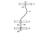
図9に示すように、プローブ10にストッパー領域100を形成してもよい。ストッパー領域100は、プローブ10のボトムガイド板22を貫通する領域よりも基端部の側に設けられた領域であり、ストッパー領域100の外径はボトムガイド板22のガイド穴220の内径よりも大きい。
第2の実施形態に係る電気的接続装置1では、プローブ10の機械的な硬度が、最大応力箇所を除いた領域よりも最大応力箇所において高い。このため、プローブ10は、最大応力箇所よりも、最大応力箇所を除いた領域において、先端部が被検査体2と接触した際に湾曲し易い構造を有する。これにより、プローブ10の全体が均一な硬度である場合に比べて、座屈したプローブ10の最も湾曲する位置が基端部の側に移動する。その結果、第2の実施形態に係る電気的接続装置1によれば、ミドルガイド板23のガイド穴230の内部を、ガイド穴230の中心線と略平行にプローブ10が摺動する。
上記のように本発明は実施形態によって記載したが、この開示の一部をなす論述及び図面はこの発明を限定するものであると理解すべきではない。この開示から当業者には様々な代替実施形態、実施例及び運用技術が明らかとなろう。
2…被検査体
10…プローブ
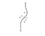
11…括れ
20…プローブヘッド
21…トップガイド板
22…ボトムガイド板
23…ミドルガイド板
30…電極基板
31…電極パッド
100…ストッパー領域
150…高硬度領域
Claims (9)
- 被検査体の電気的特性の測定に使用される電気的接続装置であって、
測定時に先端部が前記被検査体と接触するプローブと、
前記プローブの基端部に近い領域が貫通するトップガイド板、前記トップガイド板よりも前記プローブの前記先端部に近い領域が貫通するボトムガイド板、及び前記トップガイド板と前記ボトムガイド板との間で前記ボトムガイド板に近く配置されて前記プローブが貫通するミドルガイド板を有するプローブヘッドと
を備え、
前記トップガイド板の主面の面法線方向からみて、前記トップガイド板と前記ミドルガイド板とでは前記プローブが貫通するガイド穴の位置がずらして設けられており、前記プローブが前記トップガイド板と前記ミドルガイド板の間で湾曲した状態で保持され、
前記プローブが、前記先端部が前記被検査体と接触することにより座屈した前記プローブにかかる応力が最大である最大応力箇所よりも、前記最大応力箇所を除いた領域において、前記先端部が前記被検査体と接触した際に湾曲し易い構造を有する
ことを特徴とする電気的接続装置。 - 前記トップガイド板と前記ミドルガイド板の間で、前記最大応力箇所を除いた領域において前記プローブの側面に括れが形成されていることを特徴とする請求項1に記載の電気的接続装置。
- 前記プローブの全周に渡って前記括れが形成されていることを特徴とする請求項2に記載の電気的接続装置。
- 前記プローブが座屈する際に前記プローブの軸方向に伸縮する面に前記括れが形成されていることを特徴とする請求項2に記載の電気的接続装置。
- 前記プローブの機械的な硬度が、前記最大応力箇所を除いた領域よりも前記最大応力箇所において高いことを特徴とする請求項1に記載の電気的接続装置。
- 前記プローブの軸方向と垂直な断面形状が矩形状であることを特徴とする請求項1乃至5のいずれか1項に記載の電気的接続装置。
- 前記トップガイド板と前記ボトムガイド板との間に配置される前記ミドルガイド板の枚数が1枚であることを特徴とする請求項6に記載の電気的接続装置。
- 前記プローブに、前記ガイド穴の内径よりも外径が大きいストッパー領域が形成され、
前記被検査体の測定時に前記先端部が前記被検査体と接触することにより、前記ストッパー領域が前記トップガイド板、前記ボトムガイド板及び前記ミドルガイド板のいずれかに当接することを特徴とする請求項1乃至7のいずれか1項に記載の電気的接続装置。 - 前記プローブの前記ボトムガイド板を貫通する領域よりも前記基端部の側に、前記ボトムガイド板の前記ガイド穴の内径よりも外径が大きい前記ストッパー領域が形成されていることを特徴とする請求項8に記載の電気的接続装置。
Priority Applications (6)
| Application Number | Priority Date | Filing Date | Title |
|---|---|---|---|
| JP2019040144A JP7381209B2 (ja) | 2019-03-06 | 2019-03-06 | 電気的接続装置 |
| PCT/JP2020/007947 WO2020179596A1 (ja) | 2019-03-06 | 2020-02-27 | 電気的接続装置 |
| CN202080018929.0A CN113544831A (zh) | 2019-03-06 | 2020-02-27 | 电连接装置 |
| KR1020217027705A KR102623985B1 (ko) | 2019-03-06 | 2020-02-27 | 전기적 접속 장치 |
| US17/436,564 US12000867B2 (en) | 2019-03-06 | 2020-02-27 | Electrical connecting device |
| TW109107281A TWI737208B (zh) | 2019-03-06 | 2020-03-05 | 電性連接裝置 |
Applications Claiming Priority (1)
| Application Number | Priority Date | Filing Date | Title |
|---|---|---|---|
| JP2019040144A JP7381209B2 (ja) | 2019-03-06 | 2019-03-06 | 電気的接続装置 |
Publications (2)
| Publication Number | Publication Date |
|---|---|
| JP2020143976A true JP2020143976A (ja) | 2020-09-10 |
| JP7381209B2 JP7381209B2 (ja) | 2023-11-15 |
Family
ID=72337953
Family Applications (1)
| Application Number | Title | Priority Date | Filing Date |
|---|---|---|---|
| JP2019040144A Active JP7381209B2 (ja) | 2019-03-06 | 2019-03-06 | 電気的接続装置 |
Country Status (6)
| Country | Link |
|---|---|
| US (1) | US12000867B2 (ja) |
| JP (1) | JP7381209B2 (ja) |
| KR (1) | KR102623985B1 (ja) |
| CN (1) | CN113544831A (ja) |
| TW (1) | TWI737208B (ja) |
| WO (1) | WO2020179596A1 (ja) |
Cited By (3)
| Publication number | Priority date | Publication date | Assignee | Title |
|---|---|---|---|---|
| KR20230127485A (ko) * | 2022-02-25 | 2023-09-01 | (주)티에스이 | 저마찰형 프로브 헤드 |
| JP2024514988A (ja) * | 2021-04-30 | 2024-04-03 | ピーティーアンドケー カンパニー リミテッド | プローブピンとプローブピンの製造方法 |
| WO2026009835A1 (ja) * | 2024-07-03 | 2026-01-08 | 株式会社日本マイクロニクス | 電気的接続装置 |
Families Citing this family (5)
| Publication number | Priority date | Publication date | Assignee | Title |
|---|---|---|---|---|
| CN114325296A (zh) * | 2020-09-30 | 2022-04-12 | 揖斐电株式会社 | 导通检查用治具和印刷布线板的检查方法 |
| JP2023096615A (ja) * | 2021-12-27 | 2023-07-07 | 株式会社日本マイクロニクス | 電気的接続装置 |
| CN118284812A (zh) * | 2022-03-16 | 2024-07-02 | 日本电子材料株式会社 | 复合探针、探针的安装方法以及探针卡的制造方法 |
| JP2024041465A (ja) * | 2022-09-14 | 2024-03-27 | 株式会社日本マイクロニクス | 電気的接続装置 |
| CN115308456B (zh) * | 2022-09-29 | 2023-03-10 | 深圳市道格特科技有限公司 | 一种垂直探针及探针卡 |
Citations (10)
| Publication number | Priority date | Publication date | Assignee | Title |
|---|---|---|---|---|
| JP2005292019A (ja) * | 2004-04-02 | 2005-10-20 | Japan Electronic Materials Corp | プローブ |
| US20100171519A1 (en) * | 2008-06-18 | 2010-07-08 | Star Technologies Inc. | Probe and probe card for integrated circuit devices using the same |
| US20120286816A1 (en) * | 2004-05-21 | 2012-11-15 | Microprobe, Inc. | Probes with high current carrying capability and laser machining methods |
| JP2014001997A (ja) * | 2012-06-18 | 2014-01-09 | Micronics Japan Co Ltd | 垂直動作式プローブカード |
| JP2014044099A (ja) * | 2012-08-27 | 2014-03-13 | Micronics Japan Co Ltd | 電気的接続装置 |
| US20140352460A1 (en) * | 2013-06-03 | 2014-12-04 | Mpi Corporation | Probe Needle and Probe Module Using the Same |
| JP2015230314A (ja) * | 2014-06-06 | 2015-12-21 | 旺▲夕▼科技股▲分▼有限公司 | プローブおよびその製造方法 |
| JP2017521668A (ja) * | 2014-07-14 | 2017-08-03 | テクノプローベ エス.ピー.エー. | 試験ヘッドのための接触プローブ、及び対応する製造方法 |
| JP2018004260A (ja) * | 2016-06-27 | 2018-01-11 | 株式会社日本マイクロニクス | 電気的接続装置及び接触子 |
| JP2018523095A (ja) * | 2015-05-07 | 2018-08-16 | テクノプローベ エス.ピー.エー. | 特に低減ピッチ用途のための、垂直プローブを有するテストヘッド |
Family Cites Families (8)
| Publication number | Priority date | Publication date | Assignee | Title |
|---|---|---|---|---|
| US5952843A (en) * | 1998-03-24 | 1999-09-14 | Vinh; Nguyen T. | Variable contact pressure probe |
| TW200806992A (en) | 2006-07-26 | 2008-02-01 | Probeleader Co Ltd | Assembly structure of probe card |
| JP6305754B2 (ja) | 2013-12-20 | 2018-04-04 | 東京特殊電線株式会社 | コンタクトプローブユニット |
| TWM502175U (zh) * | 2015-02-04 | 2015-06-01 | Chin-Yi Lin | 探針頭 |
| WO2016146499A1 (en) * | 2015-03-13 | 2016-09-22 | Technoprobe S.P.A. | Testing head with vertical probes having an improved sliding movement within respective guide holes and correct holding of the probes within the testing head under different operative conditions |
| IT201700021397A1 (it) * | 2017-02-24 | 2018-08-24 | Technoprobe Spa | Testa di misura con migliorate proprietà in frequenza |
| JP2018179721A (ja) * | 2017-04-12 | 2018-11-15 | 株式会社日本マイクロニクス | 電気的接続装置 |
| TW201843457A (zh) * | 2017-05-05 | 2018-12-16 | 旺矽科技股份有限公司 | 具有垂直式探針之探針頭 |
-
2019
- 2019-03-06 JP JP2019040144A patent/JP7381209B2/ja active Active
-
2020
- 2020-02-27 US US17/436,564 patent/US12000867B2/en active Active
- 2020-02-27 KR KR1020217027705A patent/KR102623985B1/ko active Active
- 2020-02-27 CN CN202080018929.0A patent/CN113544831A/zh active Pending
- 2020-02-27 WO PCT/JP2020/007947 patent/WO2020179596A1/ja not_active Ceased
- 2020-03-05 TW TW109107281A patent/TWI737208B/zh active
Patent Citations (10)
| Publication number | Priority date | Publication date | Assignee | Title |
|---|---|---|---|---|
| JP2005292019A (ja) * | 2004-04-02 | 2005-10-20 | Japan Electronic Materials Corp | プローブ |
| US20120286816A1 (en) * | 2004-05-21 | 2012-11-15 | Microprobe, Inc. | Probes with high current carrying capability and laser machining methods |
| US20100171519A1 (en) * | 2008-06-18 | 2010-07-08 | Star Technologies Inc. | Probe and probe card for integrated circuit devices using the same |
| JP2014001997A (ja) * | 2012-06-18 | 2014-01-09 | Micronics Japan Co Ltd | 垂直動作式プローブカード |
| JP2014044099A (ja) * | 2012-08-27 | 2014-03-13 | Micronics Japan Co Ltd | 電気的接続装置 |
| US20140352460A1 (en) * | 2013-06-03 | 2014-12-04 | Mpi Corporation | Probe Needle and Probe Module Using the Same |
| JP2015230314A (ja) * | 2014-06-06 | 2015-12-21 | 旺▲夕▼科技股▲分▼有限公司 | プローブおよびその製造方法 |
| JP2017521668A (ja) * | 2014-07-14 | 2017-08-03 | テクノプローベ エス.ピー.エー. | 試験ヘッドのための接触プローブ、及び対応する製造方法 |
| JP2018523095A (ja) * | 2015-05-07 | 2018-08-16 | テクノプローベ エス.ピー.エー. | 特に低減ピッチ用途のための、垂直プローブを有するテストヘッド |
| JP2018004260A (ja) * | 2016-06-27 | 2018-01-11 | 株式会社日本マイクロニクス | 電気的接続装置及び接触子 |
Cited By (6)
| Publication number | Priority date | Publication date | Assignee | Title |
|---|---|---|---|---|
| JP2024514988A (ja) * | 2021-04-30 | 2024-04-03 | ピーティーアンドケー カンパニー リミテッド | プローブピンとプローブピンの製造方法 |
| JP7645593B2 (ja) | 2021-04-30 | 2025-03-14 | ピーティーアンドケー カンパニー リミテッド | プローブピンとプローブピンの製造方法 |
| JP2025071306A (ja) * | 2021-04-30 | 2025-05-02 | ピーティーアンドケー カンパニー リミテッド | プローブピンとプローブピンの製造方法 |
| KR20230127485A (ko) * | 2022-02-25 | 2023-09-01 | (주)티에스이 | 저마찰형 프로브 헤드 |
| KR102673349B1 (ko) | 2022-02-25 | 2024-06-07 | (주)티에스이 | 저마찰형 프로브 헤드 |
| WO2026009835A1 (ja) * | 2024-07-03 | 2026-01-08 | 株式会社日本マイクロニクス | 電気的接続装置 |
Also Published As
| Publication number | Publication date |
|---|---|
| WO2020179596A1 (ja) | 2020-09-10 |
| KR102623985B1 (ko) | 2024-01-11 |
| TWI737208B (zh) | 2021-08-21 |
| CN113544831A (zh) | 2021-10-22 |
| JP7381209B2 (ja) | 2023-11-15 |
| US20220146553A1 (en) | 2022-05-12 |
| US12000867B2 (en) | 2024-06-04 |
| TW202041865A (zh) | 2020-11-16 |
| KR20210123339A (ko) | 2021-10-13 |
Similar Documents
| Publication | Publication Date | Title |
|---|---|---|
| JP2020143976A (ja) | 電気的接続装置 | |
| KR102156364B1 (ko) | 전기적 접속 장치 | |
| CN104062476B (zh) | 探针卡用导板 | |
| US20020070743A1 (en) | Testing head having vertical probes | |
| CN101359000B (zh) | 电气讯号接续装置 | |
| US20160223590A1 (en) | Probe head and upper guider plate | |
| JP6872960B2 (ja) | 電気的接続装置 | |
| JP2017150864A (ja) | プローブガイド、プローブカード及びプローブガイドの製造方法 | |
| US7688089B2 (en) | Compliant membrane thin film interposer probe for intergrated circuit device testing | |
| KR20140059896A (ko) | 탐침 구조물 및 이를 갖는 프로브 카드 | |
| KR20140003761A (ko) | 정열편이 형성된 프로브핀 및 그의 프로브헤드 | |
| EP4589307A1 (en) | Electrical connection device | |
| EP4632392A1 (en) | Probe | |
| EP4632391A1 (en) | Probe and electrical connection device | |
| JP2008298678A (ja) | 電気的接続装置 | |
| JP6373011B2 (ja) | プローブカード | |
| US11959941B2 (en) | Probe card | |
| WO2023181754A1 (ja) | プローブ、プローブ保持装置およびプローブの製造方法 | |
| WO2024014231A1 (ja) | プローブ装置 | |
| JP2001330625A5 (ja) | ||
| JP2007157650A (ja) | 検査装置用ソケット |
Legal Events
| Date | Code | Title | Description |
|---|---|---|---|
| A621 | Written request for application examination |
Free format text: JAPANESE INTERMEDIATE CODE: A621 Effective date: 20220127 |
|
| A131 | Notification of reasons for refusal |
Free format text: JAPANESE INTERMEDIATE CODE: A131 Effective date: 20221004 |
|
| A521 | Request for written amendment filed |
Free format text: JAPANESE INTERMEDIATE CODE: A523 Effective date: 20221130 |
|
| A131 | Notification of reasons for refusal |
Free format text: JAPANESE INTERMEDIATE CODE: A131 Effective date: 20230307 |
|
| A521 | Request for written amendment filed |
Free format text: JAPANESE INTERMEDIATE CODE: A523 Effective date: 20230417 |
|
| A02 | Decision of refusal |
Free format text: JAPANESE INTERMEDIATE CODE: A02 Effective date: 20230613 |
|
| A521 | Request for written amendment filed |
Free format text: JAPANESE INTERMEDIATE CODE: A523 Effective date: 20230830 |
|
| A911 | Transfer to examiner for re-examination before appeal (zenchi) |
Free format text: JAPANESE INTERMEDIATE CODE: A911 Effective date: 20230911 |
|
| TRDD | Decision of grant or rejection written | ||
| A01 | Written decision to grant a patent or to grant a registration (utility model) |
Free format text: JAPANESE INTERMEDIATE CODE: A01 Effective date: 20231017 |
|
| A61 | First payment of annual fees (during grant procedure) |
Free format text: JAPANESE INTERMEDIATE CODE: A61 Effective date: 20231102 |
|
| R150 | Certificate of patent or registration of utility model |
Ref document number: 7381209 Country of ref document: JP Free format text: JAPANESE INTERMEDIATE CODE: R150 |