JP2020178067A - シリコン膜の成膜方法 - Google Patents
シリコン膜の成膜方法 Download PDFInfo
- Publication number
- JP2020178067A JP2020178067A JP2019080041A JP2019080041A JP2020178067A JP 2020178067 A JP2020178067 A JP 2020178067A JP 2019080041 A JP2019080041 A JP 2019080041A JP 2019080041 A JP2019080041 A JP 2019080041A JP 2020178067 A JP2020178067 A JP 2020178067A
- Authority
- JP
- Japan
- Prior art keywords
- gas
- silicon film
- plasma
- forming
- electrode
- Prior art date
- Legal status (The legal status is an assumption and is not a legal conclusion. Google has not performed a legal analysis and makes no representation as to the accuracy of the status listed.)
- Granted
Links
- XUIMIQQOPSSXEZ-UHFFFAOYSA-N Silicon Chemical compound [Si] XUIMIQQOPSSXEZ-UHFFFAOYSA-N 0.000 title claims abstract description 54
- 229910052710 silicon Inorganic materials 0.000 title claims abstract description 54
- 239000010703 silicon Substances 0.000 title claims abstract description 54
- 238000000151 deposition Methods 0.000 title abstract description 9
- 239000007789 gas Substances 0.000 claims abstract description 109
- UFHFLCQGNIYNRP-UHFFFAOYSA-N Hydrogen Chemical compound [H][H] UFHFLCQGNIYNRP-UHFFFAOYSA-N 0.000 claims abstract description 56
- 239000000758 substrate Substances 0.000 claims abstract description 47
- 238000000034 method Methods 0.000 claims abstract description 44
- 239000012895 dilution Substances 0.000 claims abstract description 26
- 238000010790 dilution Methods 0.000 claims abstract description 26
- 238000009616 inductively coupled plasma Methods 0.000 claims abstract description 19
- 230000015572 biosynthetic process Effects 0.000 claims description 32
- 239000002826 coolant Substances 0.000 claims description 29
- 239000011261 inert gas Substances 0.000 claims description 21
- 239000004020 conductor Substances 0.000 claims description 18
- 239000003989 dielectric material Substances 0.000 claims description 5
- 239000003085 diluting agent Substances 0.000 claims description 4
- 239000012528 membrane Substances 0.000 claims description 2
- 229910052739 hydrogen Inorganic materials 0.000 abstract description 42
- 239000001257 hydrogen Substances 0.000 abstract description 37
- 229910021417 amorphous silicon Inorganic materials 0.000 abstract description 17
- 230000008021 deposition Effects 0.000 abstract description 5
- 239000000243 solution Substances 0.000 abstract description 2
- 229910004014 SiF4 Inorganic materials 0.000 abstract 1
- ABTOQLMXBSRXSM-UHFFFAOYSA-N silicon tetrafluoride Chemical compound F[Si](F)(F)F ABTOQLMXBSRXSM-UHFFFAOYSA-N 0.000 abstract 1
- 239000010408 film Substances 0.000 description 117
- 229910052751 metal Inorganic materials 0.000 description 49
- 239000002184 metal Substances 0.000 description 49
- 239000003990 capacitor Substances 0.000 description 12
- 150000002500 ions Chemical class 0.000 description 11
- 238000002474 experimental method Methods 0.000 description 9
- 230000001965 increasing effect Effects 0.000 description 7
- 229920001940 conductive polymer Polymers 0.000 description 6
- 238000005268 plasma chemical vapour deposition Methods 0.000 description 6
- 238000000623 plasma-assisted chemical vapour deposition Methods 0.000 description 6
- 229910052786 argon Inorganic materials 0.000 description 5
- 239000000463 material Substances 0.000 description 5
- 230000007246 mechanism Effects 0.000 description 5
- KRHYYFGTRYWZRS-UHFFFAOYSA-N Fluorane Chemical compound F KRHYYFGTRYWZRS-UHFFFAOYSA-N 0.000 description 4
- 239000004696 Poly ether ether ketone Substances 0.000 description 4
- 239000004734 Polyphenylene sulfide Substances 0.000 description 4
- 238000012856 packing Methods 0.000 description 4
- 230000002093 peripheral effect Effects 0.000 description 4
- 229920002530 polyetherether ketone Polymers 0.000 description 4
- 229920000069 polyphenylene sulfide Polymers 0.000 description 4
- 239000002994 raw material Substances 0.000 description 4
- XLYOFNOQVPJJNP-UHFFFAOYSA-N water Substances O XLYOFNOQVPJJNP-UHFFFAOYSA-N 0.000 description 4
- PNEYBMLMFCGWSK-UHFFFAOYSA-N aluminium oxide Inorganic materials [O-2].[O-2].[O-2].[Al+3].[Al+3] PNEYBMLMFCGWSK-UHFFFAOYSA-N 0.000 description 3
- 230000008859 change Effects 0.000 description 3
- 238000006243 chemical reaction Methods 0.000 description 3
- 238000005229 chemical vapour deposition Methods 0.000 description 3
- 238000007865 diluting Methods 0.000 description 3
- 238000011156 evaluation Methods 0.000 description 3
- 239000002245 particle Substances 0.000 description 3
- RYGMFSIKBFXOCR-UHFFFAOYSA-N Copper Chemical compound [Cu] RYGMFSIKBFXOCR-UHFFFAOYSA-N 0.000 description 2
- 239000004698 Polyethylene Substances 0.000 description 2
- 229910045601 alloy Inorganic materials 0.000 description 2
- 239000000956 alloy Substances 0.000 description 2
- 229910052782 aluminium Inorganic materials 0.000 description 2
- XAGFODPZIPBFFR-UHFFFAOYSA-N aluminium Chemical compound [Al] XAGFODPZIPBFFR-UHFFFAOYSA-N 0.000 description 2
- 238000011109 contamination Methods 0.000 description 2
- 239000010949 copper Substances 0.000 description 2
- 229910052802 copper Inorganic materials 0.000 description 2
- 238000000354 decomposition reaction Methods 0.000 description 2
- 230000007423 decrease Effects 0.000 description 2
- 229920006351 engineering plastic Polymers 0.000 description 2
- 229910052734 helium Inorganic materials 0.000 description 2
- 150000002431 hydrogen Chemical class 0.000 description 2
- 238000009413 insulation Methods 0.000 description 2
- 239000007788 liquid Substances 0.000 description 2
- 238000004518 low pressure chemical vapour deposition Methods 0.000 description 2
- 238000004519 manufacturing process Methods 0.000 description 2
- 229910052754 neon Inorganic materials 0.000 description 2
- 229920000573 polyethylene Polymers 0.000 description 2
- 238000003825 pressing Methods 0.000 description 2
- 230000008569 process Effects 0.000 description 2
- 239000010453 quartz Substances 0.000 description 2
- 238000007789 sealing Methods 0.000 description 2
- VYPSYNLAJGMNEJ-UHFFFAOYSA-N silicon dioxide Inorganic materials O=[Si]=O VYPSYNLAJGMNEJ-UHFFFAOYSA-N 0.000 description 2
- DDFHBQSCUXNBSA-UHFFFAOYSA-N 5-(5-carboxythiophen-2-yl)thiophene-2-carboxylic acid Chemical compound S1C(C(=O)O)=CC=C1C1=CC=C(C(O)=O)S1 DDFHBQSCUXNBSA-UHFFFAOYSA-N 0.000 description 1
- YCKRFDGAMUMZLT-UHFFFAOYSA-N Fluorine atom Chemical compound [F] YCKRFDGAMUMZLT-UHFFFAOYSA-N 0.000 description 1
- 238000005033 Fourier transform infrared spectroscopy Methods 0.000 description 1
- 229910052581 Si3N4 Inorganic materials 0.000 description 1
- 238000000137 annealing Methods 0.000 description 1
- 230000037237 body shape Effects 0.000 description 1
- 239000000919 ceramic Substances 0.000 description 1
- 230000006866 deterioration Effects 0.000 description 1
- 230000000694 effects Effects 0.000 description 1
- 230000005684 electric field Effects 0.000 description 1
- 238000010292 electrical insulation Methods 0.000 description 1
- 238000004880 explosion Methods 0.000 description 1
- 229910052731 fluorine Inorganic materials 0.000 description 1
- 239000011737 fluorine Substances 0.000 description 1
- 238000010438 heat treatment Methods 0.000 description 1
- 238000005984 hydrogenation reaction Methods 0.000 description 1
- 230000006698 induction Effects 0.000 description 1
- 230000001939 inductive effect Effects 0.000 description 1
- 238000003780 insertion Methods 0.000 description 1
- 230000037431 insertion Effects 0.000 description 1
- 229910052743 krypton Inorganic materials 0.000 description 1
- 238000005224 laser annealing Methods 0.000 description 1
- 239000004973 liquid crystal related substance Substances 0.000 description 1
- 239000011259 mixed solution Substances 0.000 description 1
- 238000012986 modification Methods 0.000 description 1
- 230000004048 modification Effects 0.000 description 1
- 230000000149 penetrating effect Effects 0.000 description 1
- -1 polyethylene Polymers 0.000 description 1
- 238000006116 polymerization reaction Methods 0.000 description 1
- 230000009467 reduction Effects 0.000 description 1
- 239000003507 refrigerant Substances 0.000 description 1
- 239000011347 resin Substances 0.000 description 1
- 229920005989 resin Polymers 0.000 description 1
- HBMJWWWQQXIZIP-UHFFFAOYSA-N silicon carbide Chemical compound [Si+]#[C-] HBMJWWWQQXIZIP-UHFFFAOYSA-N 0.000 description 1
- 229910010271 silicon carbide Inorganic materials 0.000 description 1
- HQVNEWCFYHHQES-UHFFFAOYSA-N silicon nitride Chemical compound N12[Si]34N5[Si]62N3[Si]51N64 HQVNEWCFYHHQES-UHFFFAOYSA-N 0.000 description 1
- 239000010935 stainless steel Substances 0.000 description 1
- 229910001220 stainless steel Inorganic materials 0.000 description 1
- 239000010409 thin film Substances 0.000 description 1
- 230000001988 toxicity Effects 0.000 description 1
- 231100000419 toxicity Toxicity 0.000 description 1
- 229910052724 xenon Inorganic materials 0.000 description 1
Images


Landscapes
- Chemical Vapour Deposition (AREA)
Abstract
Description
CVDプラズマ成膜装置の真空槽内に載置された基板上に、プラズマを用いてアモルファス構造を有するシリコン膜を成膜するシリコン膜の成膜方法であって、
前記プラズマの生成に、主ガスとしてSiF4ガスを、希釈用ガスとして不活性ガスおよび水素ガスを用い、
前記主ガスと前記希釈用ガスとの全体に占める前記水素ガスの比率を6〜35容量%とし、
前記真空槽内に、前記主ガスおよび前記希釈用ガスを導入しながら、前記真空槽内を100mTorr以下の圧力に保持して、誘導結合型プラズマを生成させ、
300℃以下の基板上に前記シリコン膜を成膜することを特徴とするシリコン膜の成膜方法である。
前記主ガスと前記希釈用ガスとの全体に占める前記水素ガスの比率を8〜25容量%とすることを特徴とする請求項1に記載のシリコン膜の成膜方法である。
前記主ガスと前記希釈用ガスとの全体に占める前記水素ガスの比率を9〜17容量%とすることを特徴とする請求項1に記載のシリコン膜の成膜方法である。
前記主ガスと前記希釈用ガスとの全体に占める前記SiF4ガスの比率を8〜12容量%とすることを特徴とする請求項1ないし請求項3のいずれか1項に記載のシリコン膜の成膜方法である。
前記主ガスと前記希釈用ガスとの全体に占める前記不活性ガスの比率を55〜84容量%とすることを特徴とする請求項1ないし請求項4のいずれか1項に記載のシリコン膜の成膜方法である。
前記不活性ガスとして、Arガスを用いることを特徴とする請求項1ないし請求項5のいずれか1項に記載のシリコン膜の成膜方法である。
内部に冷却液が流通する流路を有し、以下の構成を有するアンテナ
・少なくとも2つの管状の導体要素
・隣り合う導体要素の間に設けられて、各導体要素を絶縁する管状の絶縁要素
・前記流路に設けられて、互いに隣り合う導体要素と電気的に直列接続された容量
素子
前記CVDプラズマ成膜装置として、
内部に冷却液が流通する流路を有し、少なくとも2つの管状をなす導体要素と、互いに隣り合う前記導体要素の間に設けられて、それら導体要素を絶縁する管状をなす絶縁要素と、前記流路に設けられて、互いに隣り合う前記導体要素と電気的に直列接続された容量素子とを有するアンテナを備え、
前記容量素子は、互いに隣り合う前記導体要素の一方と電気的に接続された第1の電極と、互いに隣り合う前記導体要素の他方と電気的に接続されるとともに、前記第1の電極に対向して配置された第2の電極と、前記第1の電極及び前記第2の電極の間の空間を満たす誘電体とからなり、
前記冷却液を前記誘電体として用いた成膜装置を用いることを特徴とする請求項1ないし請求項6のいずれか1項に記載のシリコン膜の成膜方法である。
成膜中、前記アンテナに対し、700〜1000mW/cm2のパワー密度で高周波電力を印加して前記誘導結合型プラズマを生成させることを特徴とする請求項7に記載のシリコン膜の成膜方法である。
成膜中の前記主ガスと希釈用ガスとを合わせたガスの面積当たりのトータル流量が、0.040〜0.157sccm/cm2であることを特徴とする請求項7または請求項8に記載のシリコン膜の成膜方法である。
成膜中の前記主ガスの面積当たりの流量が、0.007〜0.018sccm/cm2であることを特徴とする請求項7ないし請求項9のいずれか1項に記載のシリコン膜の成膜方法である。
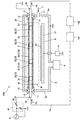
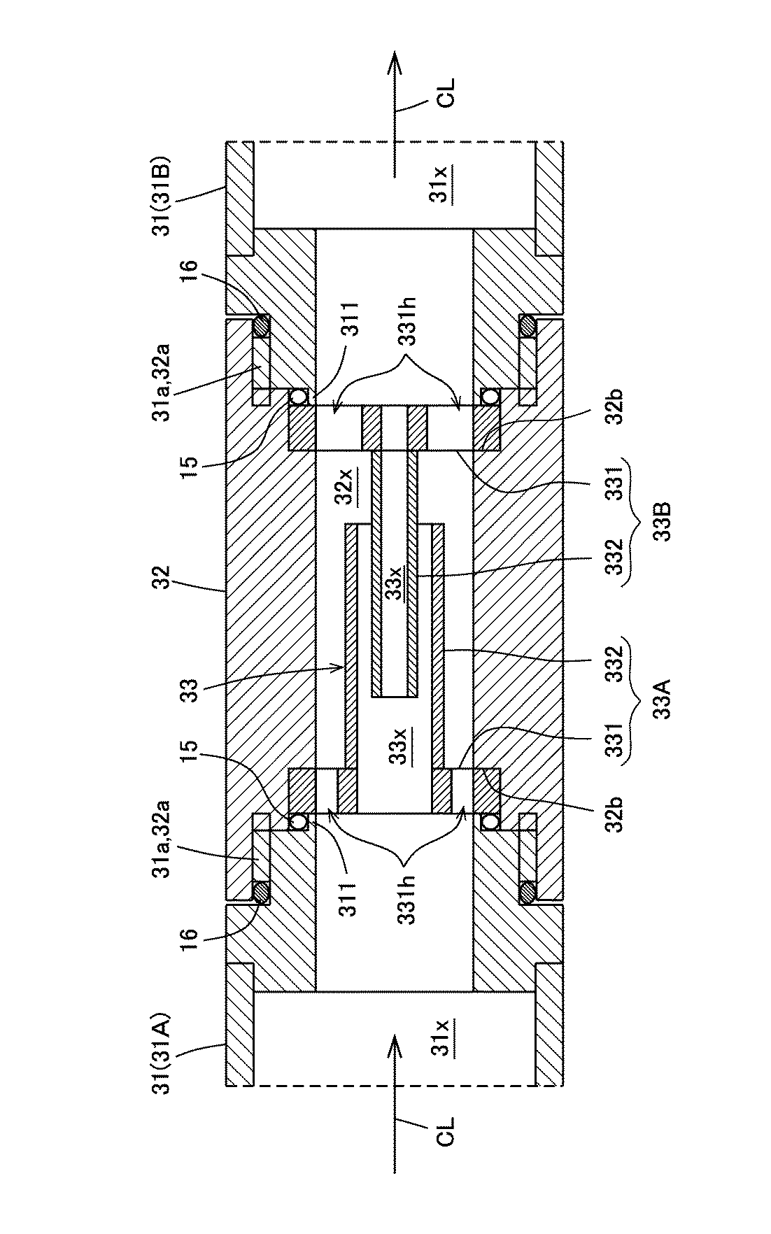
図1および図2は、本実施の形態において使用される成膜装置、即ち、上記した構成の成膜装置の模式的な断面図である。なお、図1はアンテナの長手方向に沿った縦断面図であり、図2はアンテナの長手方向と直交する方向に沿った縦断面図である。また、図3はアンテナにおけるコンデンサ部分を示す部分拡大断面図である。
このように構成した本実施形態の成膜装置100によれば、絶縁パイプ32を介して互いに隣り合う金属パイプ31にコンデンサ33を電気的に直列接続しているので、アンテナ3の合成リアクタンスは、簡単に言えば、誘導性リアクタンスから容量性リアクタンスを引いた形になるので、アンテナ3のインピーダンスを低減させることができる。その結果、アンテナ3を長くする場合でもそのインピーダンスの増大を抑えることができ、アンテナ3に高周波電流が流れやすくなり、誘導結合型のプラズマPを効率良く発生させることができる。
次に、上記した成膜装置を用いて行う本実施の形態に係るシリコン膜の成膜方法について説明する。
まず、主ガスとしてはSiF4ガスを用いる。前記した通り、SiF4は、水素(H)を含まないため、シリコン膜中にHが取り込まれ難く、水素含有比率を低くすることができる。
主ガスおよび希釈用ガスの比率については、主ガスと希釈用ガスの全体に占める水素ガスの比率が6〜35容量%となるように制御する。これにより、水素含有比率を、従来に比べて、大きく低減することができる。このとき、主ガスと希釈用ガスとの全体に占めるSiF4ガスの比率を8〜12容量%、不活性ガスの比率を55〜84容量%となるように制御することが好ましい。
真空槽内の圧力は、100mTorr以下の低い圧力に保持する。これにより、プラズマの平均自由行程を長くすることができ、プラズマを構成するイオンや電子に大きなエネルギーを加えることができる。
本実施の形態においては、プラズマとして、誘導結合型プラズマを生成させる。これにより、プラズマ化におけるガスの分解効率を向上させることができる。
成膜中、アンテナに印加する高周波電力のパワー密度は、ICP生成の観点から、700m〜1000mW/cm2であることが好ましい。なお、ここでいう「パワー密度」とは、アンテナに印加する電力(mW)を真空槽内の内部空間を基板と平行に横切るように切断した断面積(cm2)によって除した値である。より、具体的には、断面積は、真空槽の基板とアンテナとの間の内部空間を基板と平行に横切るように切断した断面積である。
主ガスと希釈用ガスとの面積当たりのトータル流量は、ICP生成の観点から、0.040〜0.157sccm/cm2であることが好ましい。
真空槽に供給する主ガスの面積当たりの流量は、0.007〜0.018sccm/cm2であることが好ましい。
1.シリコン膜の成膜
図1〜図3に示した構成を有する成膜装置を使用し、ICPを用いたプラズマCVD法により、下記の条件の下でシリコン膜を成膜した。
基板温度、基板、アンテナに印加するパワー、真空槽内の圧力およびSiF4ガス流量を基本条件として、下記の条件で固定した。また、不活性ガスにはArを用いた。なお、本実験において、主ガス(SiF4)と希釈用ガス(ArおよびH2)のトータル流量に対するSiF4の比率(SiF4/SiF4+Ar+H2)は、10容量%である。
(a)基板温度:300℃
(b)基板 :N型Siウエハー
(c)パワー :9kW(パワー密度:710mW/cm2)
(d)圧力 :45mTorr
(e)SiF4ガス流量:100sccm(0.008sccm/cm2)
ArおよびH2の流量およびガスのトータル流量に対する比率および成膜時間は、表1に記載の通りとした。なお、表1のAr、H2の流量欄に括弧書きで示した数値は、sccm/cm2を単位とする数値であり、表1には、膜厚(nm)、成膜速度(nm/min)、H濃度(×1021cm−1)を併記している。そして、実験例1以外の基板に対しては、予め、BHF(フッ酸とフッ化アンモニウムの混合液)による洗浄を行った。なお、ArおよびH2のガスのトータル流量に対する比率は、具体的には、Ar/SiF4+Ar+H2、および、H2/SiF4+Ar+H2である。
(1)水素含有比率(H/Si比)
各実験例で得られたシリコン膜について、FT−IR法を用いて水素含有比率(H/Si比)(at%)の測定を行った。結果を表2および図4に示す。なお、図4において、縦軸は水素含有比率(H/Si比)(at%)である。また、横軸は、上段がH2の流量比率(H2/(SiF4+Ar+H2))(容量%)、下段がArの流量比率(Ar/(SiF4+Ar+H2))(容量%)である。
1.シリコン膜の成膜
実験1で前記のようにH/Si比が、Arの流量比80容量%から90容量%の間で急激に上昇しているため、基本となる成膜条件を実験1と同じ条件にして、Ar流量およびH2流量を変量させて、さらに詳細な実験を行った。成膜条件を表3に示す。
実験1と同じ方法で水素含有比率(H/Si比)を測定した。評価結果を表4に示す。また、実験2の結果は実験1の結果を示した図4に併せて示す。
2a、2c 側壁
2b 上側壁
3 アンテナ
3a 給電端部
3b 終端部
4 高周波電源
6 真空排気装置
7 原料ガス
8 基板ホルダ
9 バイアス電源
10 絶縁カバー
11 絶縁部材
12、13 パッキン
14 循環流路
15 リング状多面接触子
16 シール部材
21 ガス導入口
31 金属パイプ
31A 第1の金属パイプ
31B 第2の金属パイプ
31a 雄ねじ部
31x、32x 流路
32 絶縁パイプ
32a 雌ねじ部
32b 凹部
33 コンデンサ
33A 第1の電極
33B 第2の電極
33x 主流路
41 整合回路
81 ヒータ
100 成膜装置
141 温調機構
142 循環機構
311 接触部
331 フランジ部
331h 貫通孔
332 延出部
CL 冷却液
IR 高周波電流
P プラズマ
W 基板
Claims (10)
- CVDプラズマ成膜装置の真空槽内に載置された基板上に、プラズマを用いてアモルファス構造を有するシリコン膜を成膜するシリコン膜の成膜方法であって、
前記プラズマの生成に、主ガスとしてSiF4ガスを、希釈用ガスとして不活性ガスおよび水素ガスを用い、
前記主ガスと前記希釈用ガスとの全体に占める前記水素ガスの比率を6〜35容量%とし、
前記真空槽内に、前記主ガスおよび前記希釈用ガスを導入しながら、前記真空槽内を100mTorr以下の圧力に保持して、誘導結合型プラズマを生成させ、
300℃以下の基板上に前記シリコン膜を成膜することを特徴とするシリコン膜の成膜方法。 - 前記主ガスと前記希釈用ガスとの全体に占める前記水素ガスの比率を8〜25容量%とすることを特徴とする請求項1に記載のシリコン膜の成膜方法。
- 前記主ガスと前記希釈用ガスとの全体に占める前記水素ガスの比率を9〜17容量%とすることを特徴とする請求項1に記載のシリコン膜の成膜方法。
- 前記主ガスと前記希釈用ガスとの全体に占める前記SiF4ガスの比率を8〜12容量%とすることを特徴とする請求項1ないし請求項3のいずれか1項に記載のシリコン膜の成膜方法。
- 前記主ガスと前記希釈用ガスとの全体に占める前記不活性ガスの比率を55〜84容量%とすることを特徴とする請求項1ないし請求項4のいずれか1項に記載のシリコン膜の成膜方法。
- 前記不活性ガスとして、Arガスを用いることを特徴とする請求項1ないし請求項5のいずれか1項に記載のシリコン膜の成膜方法。
- 前記CVDプラズマ成膜装置として、
内部に冷却液が流通する流路を有し、少なくとも2つの管状をなす導体要素と、互いに隣り合う前記導体要素の間に設けられて、それら導体要素を絶縁する管状をなす絶縁要素と、前記流路に設けられて、互いに隣り合う前記導体要素と電気的に直列接続された容量素子とを有するアンテナを備え、
前記容量素子は、互いに隣り合う前記導体要素の一方と電気的に接続された第1の電極と、互いに隣り合う前記導体要素の他方と電気的に接続されるとともに、前記第1の電極に対向して配置された第2の電極と、前記第1の電極及び前記第2の電極の間の空間を満たす誘電体とからなり、
前記冷却液を前記誘電体として用いた成膜装置を用いることを特徴とする請求項1ないし請求項6のいずれか1項に記載のシリコン膜の成膜方法。 - 成膜中、前記アンテナに対し、700〜1000mW/cm2のパワー密度で高周波電力を印加して前記誘導結合型プラズマを生成させることを特徴とする請求項7に記載のシリコン膜の成膜方法。
- 成膜中の前記主ガスと希釈用ガスとを合わせたガスの面積当たりのトータル流量が、0.040〜0.157sccm/cm2であることを特徴とする請求項7または請求項8に記載のシリコン膜の成膜方法。
- 成膜中の前記主ガスの面積当たりの流量が、0.007〜0.018sccm/cm2であることを特徴とする請求項7ないし請求項9のいずれか1項に記載のシリコン膜の成膜方法。
Priority Applications (1)
| Application Number | Priority Date | Filing Date | Title |
|---|---|---|---|
| JP2019080041A JP7233639B2 (ja) | 2019-04-19 | 2019-04-19 | シリコン膜の成膜方法 |
Applications Claiming Priority (1)
| Application Number | Priority Date | Filing Date | Title |
|---|---|---|---|
| JP2019080041A JP7233639B2 (ja) | 2019-04-19 | 2019-04-19 | シリコン膜の成膜方法 |
Publications (2)
| Publication Number | Publication Date |
|---|---|
| JP2020178067A true JP2020178067A (ja) | 2020-10-29 |
| JP7233639B2 JP7233639B2 (ja) | 2023-03-07 |
Family
ID=72936048
Family Applications (1)
| Application Number | Title | Priority Date | Filing Date |
|---|---|---|---|
| JP2019080041A Active JP7233639B2 (ja) | 2019-04-19 | 2019-04-19 | シリコン膜の成膜方法 |
Country Status (1)
| Country | Link |
|---|---|
| JP (1) | JP7233639B2 (ja) |
Citations (12)
| Publication number | Priority date | Publication date | Assignee | Title |
|---|---|---|---|---|
| JPS56104433A (en) * | 1980-01-16 | 1981-08-20 | Energy Conversion Devices Inc | Amorphous semiconductor corresponding to crystalline semiconductor |
| JPS57160907A (en) * | 1981-03-26 | 1982-10-04 | Agency Of Ind Science & Technol | Manufacture of amorphous silicon containing fluorine |
| JPS63222424A (ja) * | 1987-03-12 | 1988-09-16 | Canon Inc | 堆積膜形成法及び堆積膜形成装置 |
| JPS63232418A (ja) * | 1987-03-20 | 1988-09-28 | Canon Inc | 堆積膜形成法及び装置 |
| JPS63239931A (ja) * | 1987-03-27 | 1988-10-05 | Canon Inc | 堆積膜形成法 |
| JPH01289110A (ja) * | 1988-05-17 | 1989-11-21 | Canon Inc | 堆積膜形成法 |
| JPH0613131U (ja) * | 1981-03-16 | 1994-02-18 | エナージイー・コンバージヨン・デバイセス,インコーポレテツド | 半導体デバイス製造用の半導体層蒸着装置 |
| JP2002009295A (ja) * | 2000-06-23 | 2002-01-11 | Nec Corp | 薄膜トランジスタ及びその製造方法 |
| WO2011041087A2 (en) * | 2009-09-29 | 2011-04-07 | Applied Materials, Inc. | Inductively-coupled plasma (icp) resonant source element |
| JP2016526282A (ja) * | 2013-05-09 | 2016-09-01 | アプライド マテリアルズ インコーポレイテッドApplied Materials,Incorporated | エキシマレーザアニーリング後にポリシリコン品質を向上させる多層アモルファスシリコン構造 |
| JP2017003862A (ja) * | 2015-06-12 | 2017-01-05 | キヤノン株式会社 | 電子写真感光体の製造方法 |
| JP2018133326A (ja) * | 2017-02-16 | 2018-08-23 | 日新電機株式会社 | プラズマ発生用のアンテナ及びそれを備えるプラズマ処理装置 |
-
2019
- 2019-04-19 JP JP2019080041A patent/JP7233639B2/ja active Active
Patent Citations (12)
| Publication number | Priority date | Publication date | Assignee | Title |
|---|---|---|---|---|
| JPS56104433A (en) * | 1980-01-16 | 1981-08-20 | Energy Conversion Devices Inc | Amorphous semiconductor corresponding to crystalline semiconductor |
| JPH0613131U (ja) * | 1981-03-16 | 1994-02-18 | エナージイー・コンバージヨン・デバイセス,インコーポレテツド | 半導体デバイス製造用の半導体層蒸着装置 |
| JPS57160907A (en) * | 1981-03-26 | 1982-10-04 | Agency Of Ind Science & Technol | Manufacture of amorphous silicon containing fluorine |
| JPS63222424A (ja) * | 1987-03-12 | 1988-09-16 | Canon Inc | 堆積膜形成法及び堆積膜形成装置 |
| JPS63232418A (ja) * | 1987-03-20 | 1988-09-28 | Canon Inc | 堆積膜形成法及び装置 |
| JPS63239931A (ja) * | 1987-03-27 | 1988-10-05 | Canon Inc | 堆積膜形成法 |
| JPH01289110A (ja) * | 1988-05-17 | 1989-11-21 | Canon Inc | 堆積膜形成法 |
| JP2002009295A (ja) * | 2000-06-23 | 2002-01-11 | Nec Corp | 薄膜トランジスタ及びその製造方法 |
| WO2011041087A2 (en) * | 2009-09-29 | 2011-04-07 | Applied Materials, Inc. | Inductively-coupled plasma (icp) resonant source element |
| JP2016526282A (ja) * | 2013-05-09 | 2016-09-01 | アプライド マテリアルズ インコーポレイテッドApplied Materials,Incorporated | エキシマレーザアニーリング後にポリシリコン品質を向上させる多層アモルファスシリコン構造 |
| JP2017003862A (ja) * | 2015-06-12 | 2017-01-05 | キヤノン株式会社 | 電子写真感光体の製造方法 |
| JP2018133326A (ja) * | 2017-02-16 | 2018-08-23 | 日新電機株式会社 | プラズマ発生用のアンテナ及びそれを備えるプラズマ処理装置 |
Also Published As
| Publication number | Publication date |
|---|---|
| JP7233639B2 (ja) | 2023-03-07 |
Similar Documents
| Publication | Publication Date | Title |
|---|---|---|
| US8974684B2 (en) | Synchronous embedded radio frequency pulsing for plasma etching | |
| US8898889B2 (en) | Chuck assembly for plasma processing | |
| US20200161097A1 (en) | Peripheral rf feed and symmetric rf return for symmetric rf delivery | |
| TWI645442B (zh) | Plasma processing device | |
| KR101957348B1 (ko) | 플라즈마 처리 장치 및 플라즈마 처리 방법 | |
| TWI290809B (en) | Procedure and device for the production of a plasma | |
| US11430636B2 (en) | Plasma processing apparatus and cleaning method | |
| JP6341329B1 (ja) | プラズマ発生用のアンテナ及びそれを備えるプラズマ処理装置 | |
| JPWO2009107718A1 (ja) | プラズマエッチング処理装置およびプラズマエッチング処理方法 | |
| JP2021088727A (ja) | 成膜方法 | |
| US20110094683A1 (en) | Rf feed structure for plasma processing | |
| CN110709533A (zh) | 溅射装置 | |
| CN110291847A (zh) | 等离子体产生用的天线、具有所述天线的等离子体处理装置以及天线构造 | |
| US12154790B2 (en) | Etching method and plasma processing apparatus | |
| EP2863416B1 (en) | Method for etching copper layer | |
| JP7233639B2 (ja) | シリコン膜の成膜方法 | |
| US20180047542A1 (en) | Inductively coupled plasma chamber having a multi-zone showerhead | |
| KR102578780B1 (ko) | 반도체 제조 장치 및 반도체 장치의 제조 방법 | |
| TW202301465A (zh) | 蝕刻方法及電漿處理系統 | |
| US11368003B2 (en) | Seamless electrical conduit | |
| JP6807777B2 (ja) | プラズマ処理装置 | |
| WO2013078152A1 (en) | Peripheral rf feed and symmetric rf return with rf strap input | |
| WO2013078346A1 (en) | Peripheral rf feed and symmetric rf return for symmetric rf delivery | |
| JP7028001B2 (ja) | 成膜方法 | |
| WO2019181776A1 (ja) | アンテナ及びプラズマ処理装置 |
Legal Events
| Date | Code | Title | Description |
|---|---|---|---|
| A621 | Written request for application examination |
Free format text: JAPANESE INTERMEDIATE CODE: A621 Effective date: 20220411 |
|
| TRDD | Decision of grant or rejection written | ||
| A01 | Written decision to grant a patent or to grant a registration (utility model) |
Free format text: JAPANESE INTERMEDIATE CODE: A01 Effective date: 20230123 |
|
| A977 | Report on retrieval |
Free format text: JAPANESE INTERMEDIATE CODE: A971007 Effective date: 20230125 |
|
| A61 | First payment of annual fees (during grant procedure) |
Free format text: JAPANESE INTERMEDIATE CODE: A61 Effective date: 20230205 |
|
| R150 | Certificate of patent or registration of utility model |
Ref document number: 7233639 Country of ref document: JP Free format text: JAPANESE INTERMEDIATE CODE: R150 |