JP2020178079A - 半導体装置および表示装置 - Google Patents
半導体装置および表示装置 Download PDFInfo
- Publication number
- JP2020178079A JP2020178079A JP2019080382A JP2019080382A JP2020178079A JP 2020178079 A JP2020178079 A JP 2020178079A JP 2019080382 A JP2019080382 A JP 2019080382A JP 2019080382 A JP2019080382 A JP 2019080382A JP 2020178079 A JP2020178079 A JP 2020178079A
- Authority
- JP
- Japan
- Prior art keywords
- semiconductor
- film
- electrode
- insulating film
- low resistance
- Prior art date
- Legal status (The legal status is an assumption and is not a legal conclusion. Google has not performed a legal analysis and makes no representation as to the accuracy of the status listed.)
- Pending
Links
Images








Classifications
-
- H—ELECTRICITY
- H10—SEMICONDUCTOR DEVICES; ELECTRIC SOLID-STATE DEVICES NOT OTHERWISE PROVIDED FOR
- H10D—INORGANIC ELECTRIC SEMICONDUCTOR DEVICES
- H10D30/00—Field-effect transistors [FET]
- H10D30/60—Insulated-gate field-effect transistors [IGFET]
- H10D30/67—Thin-film transistors [TFT]
- H10D30/6704—Thin-film transistors [TFT] having supplementary regions or layers in the thin films or in the insulated bulk substrates for controlling properties of the device
-
- H—ELECTRICITY
- H10—SEMICONDUCTOR DEVICES; ELECTRIC SOLID-STATE DEVICES NOT OTHERWISE PROVIDED FOR
- H10D—INORGANIC ELECTRIC SEMICONDUCTOR DEVICES
- H10D30/00—Field-effect transistors [FET]
- H10D30/60—Insulated-gate field-effect transistors [IGFET]
- H10D30/67—Thin-film transistors [TFT]
- H10D30/674—Thin-film transistors [TFT] characterised by the active materials
- H10D30/6741—Group IV materials, e.g. germanium or silicon carbide
- H10D30/6743—Silicon
-
- H—ELECTRICITY
- H10—SEMICONDUCTOR DEVICES; ELECTRIC SOLID-STATE DEVICES NOT OTHERWISE PROVIDED FOR
- H10D—INORGANIC ELECTRIC SEMICONDUCTOR DEVICES
- H10D30/00—Field-effect transistors [FET]
- H10D30/60—Insulated-gate field-effect transistors [IGFET]
- H10D30/67—Thin-film transistors [TFT]
- H10D30/674—Thin-film transistors [TFT] characterised by the active materials
- H10D30/6755—Oxide semiconductors, e.g. zinc oxide, copper aluminium oxide or cadmium stannate
-
- H—ELECTRICITY
- H10—SEMICONDUCTOR DEVICES; ELECTRIC SOLID-STATE DEVICES NOT OTHERWISE PROVIDED FOR
- H10D—INORGANIC ELECTRIC SEMICONDUCTOR DEVICES
- H10D30/00—Field-effect transistors [FET]
- H10D30/60—Insulated-gate field-effect transistors [IGFET]
- H10D30/67—Thin-film transistors [TFT]
- H10D30/6757—Thin-film transistors [TFT] characterised by the structure of the channel, e.g. transverse or longitudinal shape or doping profile
-
- H—ELECTRICITY
- H10—SEMICONDUCTOR DEVICES; ELECTRIC SOLID-STATE DEVICES NOT OTHERWISE PROVIDED FOR
- H10D—INORGANIC ELECTRIC SEMICONDUCTOR DEVICES
- H10D62/00—Semiconductor bodies, or regions thereof, of devices having potential barriers
- H10D62/80—Semiconductor bodies, or regions thereof, of devices having potential barriers characterised by the materials
- H10D62/81—Semiconductor bodies, or regions thereof, of devices having potential barriers characterised by the materials of structures exhibiting quantum-confinement effects, e.g. single quantum wells; of structures having periodic or quasi-periodic potential variation
-
- H—ELECTRICITY
- H10—SEMICONDUCTOR DEVICES; ELECTRIC SOLID-STATE DEVICES NOT OTHERWISE PROVIDED FOR
- H10D—INORGANIC ELECTRIC SEMICONDUCTOR DEVICES
- H10D86/00—Integrated devices formed in or on insulating or conducting substrates, e.g. formed in silicon-on-insulator [SOI] substrates or on stainless steel or glass substrates
- H10D86/40—Integrated devices formed in or on insulating or conducting substrates, e.g. formed in silicon-on-insulator [SOI] substrates or on stainless steel or glass substrates characterised by multiple TFTs
- H10D86/421—Integrated devices formed in or on insulating or conducting substrates, e.g. formed in silicon-on-insulator [SOI] substrates or on stainless steel or glass substrates characterised by multiple TFTs having a particular composition, shape or crystalline structure of the active layer
- H10D86/423—Integrated devices formed in or on insulating or conducting substrates, e.g. formed in silicon-on-insulator [SOI] substrates or on stainless steel or glass substrates characterised by multiple TFTs having a particular composition, shape or crystalline structure of the active layer comprising semiconductor materials not belonging to the Group IV, e.g. InGaZnO
-
- H—ELECTRICITY
- H10—SEMICONDUCTOR DEVICES; ELECTRIC SOLID-STATE DEVICES NOT OTHERWISE PROVIDED FOR
- H10D—INORGANIC ELECTRIC SEMICONDUCTOR DEVICES
- H10D86/00—Integrated devices formed in or on insulating or conducting substrates, e.g. formed in silicon-on-insulator [SOI] substrates or on stainless steel or glass substrates
- H10D86/40—Integrated devices formed in or on insulating or conducting substrates, e.g. formed in silicon-on-insulator [SOI] substrates or on stainless steel or glass substrates characterised by multiple TFTs
- H10D86/441—Interconnections, e.g. scanning lines
-
- H—ELECTRICITY
- H10—SEMICONDUCTOR DEVICES; ELECTRIC SOLID-STATE DEVICES NOT OTHERWISE PROVIDED FOR
- H10D—INORGANIC ELECTRIC SEMICONDUCTOR DEVICES
- H10D86/00—Integrated devices formed in or on insulating or conducting substrates, e.g. formed in silicon-on-insulator [SOI] substrates or on stainless steel or glass substrates
- H10D86/40—Integrated devices formed in or on insulating or conducting substrates, e.g. formed in silicon-on-insulator [SOI] substrates or on stainless steel or glass substrates characterised by multiple TFTs
- H10D86/451—Integrated devices formed in or on insulating or conducting substrates, e.g. formed in silicon-on-insulator [SOI] substrates or on stainless steel or glass substrates characterised by multiple TFTs characterised by the compositions or shapes of the interlayer dielectrics
-
- H—ELECTRICITY
- H10—SEMICONDUCTOR DEVICES; ELECTRIC SOLID-STATE DEVICES NOT OTHERWISE PROVIDED FOR
- H10D—INORGANIC ELECTRIC SEMICONDUCTOR DEVICES
- H10D86/00—Integrated devices formed in or on insulating or conducting substrates, e.g. formed in silicon-on-insulator [SOI] substrates or on stainless steel or glass substrates
- H10D86/40—Integrated devices formed in or on insulating or conducting substrates, e.g. formed in silicon-on-insulator [SOI] substrates or on stainless steel or glass substrates characterised by multiple TFTs
- H10D86/481—Integrated devices formed in or on insulating or conducting substrates, e.g. formed in silicon-on-insulator [SOI] substrates or on stainless steel or glass substrates characterised by multiple TFTs integrated with passive devices, e.g. auxiliary capacitors
-
- H—ELECTRICITY
- H10—SEMICONDUCTOR DEVICES; ELECTRIC SOLID-STATE DEVICES NOT OTHERWISE PROVIDED FOR
- H10D—INORGANIC ELECTRIC SEMICONDUCTOR DEVICES
- H10D86/00—Integrated devices formed in or on insulating or conducting substrates, e.g. formed in silicon-on-insulator [SOI] substrates or on stainless steel or glass substrates
- H10D86/40—Integrated devices formed in or on insulating or conducting substrates, e.g. formed in silicon-on-insulator [SOI] substrates or on stainless steel or glass substrates characterised by multiple TFTs
- H10D86/60—Integrated devices formed in or on insulating or conducting substrates, e.g. formed in silicon-on-insulator [SOI] substrates or on stainless steel or glass substrates characterised by multiple TFTs wherein the TFTs are in active matrices
-
- H—ELECTRICITY
- H10—SEMICONDUCTOR DEVICES; ELECTRIC SOLID-STATE DEVICES NOT OTHERWISE PROVIDED FOR
- H10P—GENERIC PROCESSES OR APPARATUS FOR THE MANUFACTURE OR TREATMENT OF DEVICES COVERED BY CLASS H10
- H10P14/00—Formation of materials, e.g. in the shape of layers or pillars
- H10P14/60—Formation of materials, e.g. in the shape of layers or pillars of insulating materials
- H10P14/69—Inorganic materials
- H10P14/692—Inorganic materials composed of oxides, glassy oxides or oxide-based glasses
- H10P14/6921—Inorganic materials composed of oxides, glassy oxides or oxide-based glasses containing silicon
- H10P14/69215—Inorganic materials composed of oxides, glassy oxides or oxide-based glasses containing silicon the material being a silicon oxide, e.g. SiO2
-
- H—ELECTRICITY
- H10—SEMICONDUCTOR DEVICES; ELECTRIC SOLID-STATE DEVICES NOT OTHERWISE PROVIDED FOR
- H10P—GENERIC PROCESSES OR APPARATUS FOR THE MANUFACTURE OR TREATMENT OF DEVICES COVERED BY CLASS H10
- H10P14/00—Formation of materials, e.g. in the shape of layers or pillars
- H10P14/60—Formation of materials, e.g. in the shape of layers or pillars of insulating materials
- H10P14/69—Inorganic materials
- H10P14/692—Inorganic materials composed of oxides, glassy oxides or oxide-based glasses
- H10P14/6938—Inorganic materials composed of oxides, glassy oxides or oxide-based glasses the material containing at least one metal element, e.g. metal oxides, metal oxynitrides or metal oxycarbides
- H10P14/6939—Inorganic materials composed of oxides, glassy oxides or oxide-based glasses the material containing at least one metal element, e.g. metal oxides, metal oxynitrides or metal oxycarbides characterised by the metal
- H10P14/69391—Inorganic materials composed of oxides, glassy oxides or oxide-based glasses the material containing at least one metal element, e.g. metal oxides, metal oxynitrides or metal oxycarbides characterised by the metal the material containing aluminium, e.g. Al2O3
-
- H—ELECTRICITY
- H10—SEMICONDUCTOR DEVICES; ELECTRIC SOLID-STATE DEVICES NOT OTHERWISE PROVIDED FOR
- H10P—GENERIC PROCESSES OR APPARATUS FOR THE MANUFACTURE OR TREATMENT OF DEVICES COVERED BY CLASS H10
- H10P14/00—Formation of materials, e.g. in the shape of layers or pillars
- H10P14/60—Formation of materials, e.g. in the shape of layers or pillars of insulating materials
- H10P14/69—Inorganic materials
- H10P14/694—Inorganic materials composed of nitrides
- H10P14/6943—Inorganic materials composed of nitrides containing silicon
- H10P14/69433—Inorganic materials composed of nitrides containing silicon the material being a silicon nitride not containing oxygen, e.g. SixNy or SixByNz
-
- G—PHYSICS
- G02—OPTICS
- G02F—OPTICAL DEVICES OR ARRANGEMENTS FOR THE CONTROL OF LIGHT BY MODIFICATION OF THE OPTICAL PROPERTIES OF THE MEDIA OF THE ELEMENTS INVOLVED THEREIN; NON-LINEAR OPTICS; FREQUENCY-CHANGING OF LIGHT; OPTICAL LOGIC ELEMENTS; OPTICAL ANALOGUE/DIGITAL CONVERTERS
- G02F1/00—Devices or arrangements for the control of the intensity, colour, phase, polarisation or direction of light arriving from an independent light source, e.g. switching, gating or modulating; Non-linear optics
- G02F1/01—Devices or arrangements for the control of the intensity, colour, phase, polarisation or direction of light arriving from an independent light source, e.g. switching, gating or modulating; Non-linear optics for the control of the intensity, phase, polarisation or colour
- G02F1/13—Devices or arrangements for the control of the intensity, colour, phase, polarisation or direction of light arriving from an independent light source, e.g. switching, gating or modulating; Non-linear optics for the control of the intensity, phase, polarisation or colour based on liquid crystals, e.g. single liquid crystal display cells
- G02F1/133—Constructional arrangements; Operation of liquid crystal cells; Circuit arrangements
- G02F1/136—Liquid crystal cells structurally associated with a semi-conducting layer or substrate, e.g. cells forming part of an integrated circuit
- G02F1/1362—Active matrix addressed cells
- G02F1/136213—Storage capacitors associated with the pixel electrode
Landscapes
- Physics & Mathematics (AREA)
- Nonlinear Science (AREA)
- Engineering & Computer Science (AREA)
- Crystallography & Structural Chemistry (AREA)
- Mathematical Physics (AREA)
- Chemical & Material Sciences (AREA)
- Microelectronics & Electronic Packaging (AREA)
- Power Engineering (AREA)
- General Physics & Mathematics (AREA)
- Optics & Photonics (AREA)
- Thin Film Transistor (AREA)
- Semiconductor Integrated Circuits (AREA)
- Liquid Crystal (AREA)
- Electroluminescent Light Sources (AREA)
Abstract
Description
[構成]
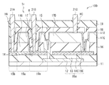
図1は、本技術の一実施の形態に係る半導体装置(半導体装置1)の断面構成を模式的に表したものである。半導体装置1は、例えば表示装置および撮像装置(後述の図7の表示装置2Aおよび図8の撮像装置2B)等の駆動回路に用いられるものである。この半導体装置1には、トップゲート型の薄膜トランジスタ(トランジスタTr)および保持容量(保持容量Cs)が設けられ、トランジスタTrと保持容量Csとが電気的に接続されている。
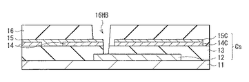
第1電極12は、基板11上の選択的な領域に設けられている。第1電極12は、第2電極15Cに対向する部分と、第2電極15Cに非対向の部分とを含んでいる。第1電極12のうち、第2電極15Cに非対向の部分は、第2電極15CよりもトランジスタTr側(図1のX軸方向)に設けられており、孔部16HBに対向している。第1電極12は、例えば、モリブデン(Mo),タングステン(W),アルミニウム(Al),銅(Cu),銀(Ag)およびチタン(Ti)等の金属を含んで構成されている。第1電極12は、合金により構成されていてもよく、複数の金属膜を含む積層膜により構成されていてもよい。第1電極12は、金属以外の導電性材料により構成されていてもよい。
図2(A)(B)は、トランジスタTrの構成を模式的に表している。図2(A)は、トランジスタTrの断面構成を表し、図2(B)は、トランジスタTrの平面構成を表している。
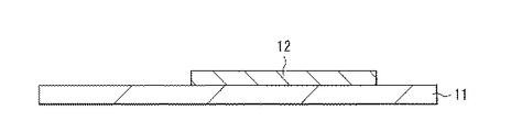
上記のような半導体装置1は、例えば次のようにして製造することができる(図4A〜図4F)。
本実施の形態の半導体装置1では、ゲート電極17に閾値電圧以上のオン電圧が印加されると、半導体膜15のチャネル領域15aが活性化される。これにより、一対の低抵抗領域15b間に電流が流れる。これに応じて、接続配線17Bを介して、半導体膜15から第1電極12に電流が流れ保持容量Csに電荷が保持される。
上記実施の形態において説明した半導体装置1は、例えば表示装置(後述の図7の表示装置2A)および撮像装置(後述の図8の撮像装置2B)等の駆動回路に用いることができる。
上記表示装置2Aおよび撮像装置2B等は、様々なタイプの電子機器に用いることができる。図9に、電子機器3の機能ブロック構成を示す。電子機器3としては、例えばテレビジョン装置、パーソナルコンピュータ(PC)、スマートフォン、タブレット型PC、携帯電話機、デジタルスチルカメラおよびデジタルビデオカメラ等が挙げられる。
(1)
基板と、
前記基板上の選択的な領域に設けられた第1半導体補助膜と、
酸化物半導体材料を含むともに、前記第1半導体補助膜に接する低抵抗領域と、前記低抵抗領域と異なる部分に設けられたチャネル領域とを有する半導体膜と、
前記半導体膜を前記チャネル領域から前記低抵抗領域の少なくとも一部まで覆うゲート絶縁膜と、
前記ゲート絶縁膜を間にして前記半導体膜の前記チャネル領域に対向するゲート電極と
を備えた半導体装置。
(2)
前記第1半導体補助膜は、前記半導体膜の前記低抵抗領域を介した電流の流れを促す
前記(1)に記載の半導体装置。
(3)
更に、前記半導体膜の前記低抵抗領域に対向する位置に設けられるとともに、前記ゲート絶縁膜を貫通する孔部と、
前記孔部を介して前記半導体膜の前記低抵抗領域に電気的に接続されたソース・ドレイン電極とを有する
前記(1)または(2)に記載の半導体装置。
(4)
前記基板上に、前記第1半導体補助膜、前記半導体膜、前記ゲート絶縁膜、前記ゲート電極および前記ソース・ドレイン電極の順に設けられている
前記(3)に記載の半導体装置。
(5)
前記第1半導体補助膜は金属を含む
前記(1)ないし(4)のうちいずれか1つに記載の半導体装置。
(6)
前記第1半導体補助膜はアルミニウムを含む
前記(1)ないし(5)のうちいずれか1つに記載の半導体装置。
(7)
前記第1半導体補助膜は金属酸化物を含む
前記(1)ないし(4)のうちいずれか1つに記載の半導体装置。
(8)
前記第1半導体補助膜は、酸化インジウムスズ(Indium Tin Oxide)または酸化インジウム亜鉛(Indium Zinc Oxide)を含む
前記(1)ないし(4)のうちいずれか1つに記載の半導体装置。
(9)
更に、
前記基板上に設けられるとともに、前記半導体膜の前記低抵抗領域に電気的に接続された第1電極と、
前記酸化物半導体材料を含むとともに、前記第1電極の少なくとも一部に対向して設けられた第2電極と、
前記第1半導体補助膜の構成材料と同じ材料を含むとともに、前記第2電極に接する第2半導体補助膜とを有する
前記(1)ないし(8)のうちいずれか1つ記載の半導体装置。
(10)
前記基板上に、前記第1電極、前記第2半導体補助膜および前記第2電極の順に設けられている
前記(9)に記載の半導体装置。
(11)
表示素子および前記表示素子を駆動する半導体装置を備え、
前記半導体装置は、
基板と、
前記基板上の選択的な領域に設けられた第1半導体補助膜と、
酸化物半導体材料を含むともに、前記第1半導体補助膜に接する低抵抗領域と、前記低抵抗領域と異なる部分に設けられたチャネル領域とを有する半導体膜と、
前記半導体膜を前記チャネル領域から前記低抵抗領域の少なくとも一部まで覆うゲート絶縁膜と、
前記ゲート絶縁膜を間にして前記半導体膜の前記チャネル領域に対向するゲート電極とを含む
表示装置。
Claims (11)
- 基板と、
前記基板上の選択的な領域に設けられた第1半導体補助膜と、
酸化物半導体材料を含むともに、前記第1半導体補助膜に接する低抵抗領域と、前記低抵抗領域と異なる部分に設けられたチャネル領域とを有する半導体膜と、
前記半導体膜を前記チャネル領域から前記低抵抗領域の少なくとも一部まで覆うゲート絶縁膜と、
前記ゲート絶縁膜を間にして前記半導体膜の前記チャネル領域に対向するゲート電極と
を備えた半導体装置。 - 前記第1半導体補助膜は、前記半導体膜の前記低抵抗領域を介した電流の流れを促す
請求項1に記載の半導体装置。 - 更に、前記半導体膜の前記低抵抗領域に対向する位置に設けられるとともに、前記ゲート絶縁膜を貫通する孔部と、
前記孔部を介して前記半導体膜の前記低抵抗領域に電気的に接続されたソース・ドレイン電極とを有する
請求項1に記載の半導体装置。 - 前記基板上に、前記第1半導体補助膜、前記半導体膜、前記ゲート絶縁膜、前記ゲート電極および前記ソース・ドレイン電極の順に設けられている
請求項3に記載の半導体装置。 - 前記第1半導体補助膜は金属を含む
請求項1に記載の半導体装置。 - 前記第1半導体補助膜はアルミニウムを含む
請求項1に記載の半導体装置。 - 前記第1半導体補助膜は金属酸化物を含む
請求項1に記載の半導体装置。 - 前記第1半導体補助膜は、酸化インジウムスズ(Indium Tin Oxide)または酸化インジウム亜鉛(Indium Zinc Oxide)を含む
請求項1に記載の半導体装置。 - 更に、
前記基板上に設けられるとともに、前記半導体膜の前記低抵抗領域に電気的に接続された第1電極と、
前記酸化物半導体材料を含むとともに、前記第1電極の少なくとも一部に対向して設けられた第2電極と、
前記第1半導体補助膜の構成材料と同じ材料を含むとともに、前記第2電極に接する第2半導体補助膜とを有する
請求項1記載の半導体装置。 - 前記基板上に、前記第1電極、前記第2半導体補助膜および前記第2電極の順に設けられている
請求項9に記載の半導体装置。 - 表示素子および前記表示素子を駆動する半導体装置を備え、
前記半導体装置は、
基板と、
前記基板上の選択的な領域に設けられた第1半導体補助膜と、
酸化物半導体材料を含むともに、前記第1半導体補助膜に接する低抵抗領域と、前記低抵抗領域と異なる部分に設けられたチャネル領域とを有する半導体膜と、
前記半導体膜を前記チャネル領域から前記低抵抗領域の少なくとも一部まで覆うゲート絶縁膜と、
前記ゲート絶縁膜を間にして前記半導体膜の前記チャネル領域に対向するゲート電極とを含む
表示装置。
Priority Applications (2)
| Application Number | Priority Date | Filing Date | Title |
|---|---|---|---|
| JP2019080382A JP2020178079A (ja) | 2019-04-19 | 2019-04-19 | 半導体装置および表示装置 |
| US16/736,814 US11081591B2 (en) | 2019-04-19 | 2020-01-08 | Semiconductor device and display unit |
Applications Claiming Priority (1)
| Application Number | Priority Date | Filing Date | Title |
|---|---|---|---|
| JP2019080382A JP2020178079A (ja) | 2019-04-19 | 2019-04-19 | 半導体装置および表示装置 |
Publications (2)
| Publication Number | Publication Date |
|---|---|
| JP2020178079A true JP2020178079A (ja) | 2020-10-29 |
| JP2020178079A5 JP2020178079A5 (ja) | 2021-12-23 |
Family
ID=72831291
Family Applications (1)
| Application Number | Title | Priority Date | Filing Date |
|---|---|---|---|
| JP2019080382A Pending JP2020178079A (ja) | 2019-04-19 | 2019-04-19 | 半導体装置および表示装置 |
Country Status (2)
| Country | Link |
|---|---|
| US (1) | US11081591B2 (ja) |
| JP (1) | JP2020178079A (ja) |
Citations (3)
| Publication number | Priority date | Publication date | Assignee | Title |
|---|---|---|---|---|
| US20130126868A1 (en) * | 2011-11-18 | 2013-05-23 | Semiconductor Energy Laboratory Co., Ltd. | Semiconductor element, method for manufacturing semiconductor element, and semiconductor device including semiconductor element |
| JP2016057547A (ja) * | 2014-09-11 | 2016-04-21 | シャープ株式会社 | Memsディスプレイおよびその製造方法 |
| JP2017228802A (ja) * | 2011-04-22 | 2017-12-28 | 株式会社半導体エネルギー研究所 | 半導体装置 |
Family Cites Families (3)
| Publication number | Priority date | Publication date | Assignee | Title |
|---|---|---|---|---|
| WO2007032128A1 (ja) | 2005-09-16 | 2007-03-22 | Sharp Kabushiki Kaisha | 薄膜トランジスタ |
| WO2015132694A1 (en) * | 2014-03-07 | 2015-09-11 | Semiconductor Energy Laboratory Co., Ltd. | Touch sensor, touch panel, and manufacturing method of touch panel |
| KR102437450B1 (ko) * | 2014-06-13 | 2022-08-30 | 가부시키가이샤 한도오따이 에네루기 켄큐쇼 | 반도체 장치, 및 반도체 장치를 포함하는 전자 기기 |
-
2019
- 2019-04-19 JP JP2019080382A patent/JP2020178079A/ja active Pending
-
2020
- 2020-01-08 US US16/736,814 patent/US11081591B2/en active Active
Patent Citations (4)
| Publication number | Priority date | Publication date | Assignee | Title |
|---|---|---|---|---|
| JP2017228802A (ja) * | 2011-04-22 | 2017-12-28 | 株式会社半導体エネルギー研究所 | 半導体装置 |
| US20130126868A1 (en) * | 2011-11-18 | 2013-05-23 | Semiconductor Energy Laboratory Co., Ltd. | Semiconductor element, method for manufacturing semiconductor element, and semiconductor device including semiconductor element |
| JP2017152720A (ja) * | 2011-11-18 | 2017-08-31 | 株式会社半導体エネルギー研究所 | 半導体装置 |
| JP2016057547A (ja) * | 2014-09-11 | 2016-04-21 | シャープ株式会社 | Memsディスプレイおよびその製造方法 |
Also Published As
| Publication number | Publication date |
|---|---|
| US20200335627A1 (en) | 2020-10-22 |
| US11081591B2 (en) | 2021-08-03 |
Similar Documents
| Publication | Publication Date | Title |
|---|---|---|
| JP6706570B2 (ja) | 半導体装置、半導体装置の製造方法および表示装置 | |
| US10886411B2 (en) | Semiconductor device and display unit | |
| US10879329B2 (en) | Semiconductor device, semiconductor substrate, luminescent unit, and display unit | |
| US11189735B2 (en) | Semiconductor device and display apparatus | |
| JP2021197416A (ja) | 半導体装置の製造方法、及び、半導体装置 | |
| US10431603B2 (en) | Semiconductor device | |
| US20170053947A1 (en) | Thin-film transistor, semiconductor unit, and electronic apparatus | |
| JP2020178079A (ja) | 半導体装置および表示装置 | |
| JP6811096B2 (ja) | 半導体装置、表示装置および電子機器 | |
| JP6732829B2 (ja) | 半導体装置および表示装置 | |
| JP2020136506A (ja) | 半導体装置、表示装置および半導体装置の製造方法 | |
| US11239371B2 (en) | Thin-film transistor including source-drain electrodes connected to a semiconducting film and extending through a semiconductor auxiliary film | |
| JP6706587B2 (ja) | 半導体装置、表示装置および電子機器 | |
| JP2019192851A (ja) | 半導体装置 | |
| JP6732713B2 (ja) | 半導体装置および表示装置 | |
| US11127762B2 (en) | Semiconductor device and display including wiring line having protective metal film | |
| JP7598749B2 (ja) | 半導体装置 | |
| JP6781051B2 (ja) | 半導体装置、表示装置および電子機器 | |
| JP2018170319A (ja) | 半導体装置およびその製造方法、並びに表示装置 | |
| JP6795543B2 (ja) | 半導体装置の製造方法 | |
| US10879402B2 (en) | Thin film transistor and display unit | |
| JP2018160518A (ja) | 半導体装置、表示装置および電子機器 | |
| JP2018195630A (ja) | トランジスタおよび表示装置 | |
| JP2018129431A (ja) | 電子デバイス、半導体装置および表示装置 |
Legal Events
| Date | Code | Title | Description |
|---|---|---|---|
| A521 | Request for written amendment filed |
Free format text: JAPANESE INTERMEDIATE CODE: A523 Effective date: 20211112 |
|
| A621 | Written request for application examination |
Free format text: JAPANESE INTERMEDIATE CODE: A621 Effective date: 20211112 |
|
| A977 | Report on retrieval |
Free format text: JAPANESE INTERMEDIATE CODE: A971007 Effective date: 20221130 |
|
| A131 | Notification of reasons for refusal |
Free format text: JAPANESE INTERMEDIATE CODE: A131 Effective date: 20221206 |
|
| A02 | Decision of refusal |
Free format text: JAPANESE INTERMEDIATE CODE: A02 Effective date: 20230530 |
|
| A711 | Notification of change in applicant |
Free format text: JAPANESE INTERMEDIATE CODE: A711 Effective date: 20230828 |
|
| A521 | Request for written amendment filed |
Free format text: JAPANESE INTERMEDIATE CODE: A821 Effective date: 20230828 |