JP2020201401A - 光学デバイス、光学デバイスの製造方法及び電子機器 - Google Patents
光学デバイス、光学デバイスの製造方法及び電子機器 Download PDFInfo
- Publication number
- JP2020201401A JP2020201401A JP2019108544A JP2019108544A JP2020201401A JP 2020201401 A JP2020201401 A JP 2020201401A JP 2019108544 A JP2019108544 A JP 2019108544A JP 2019108544 A JP2019108544 A JP 2019108544A JP 2020201401 A JP2020201401 A JP 2020201401A
- Authority
- JP
- Japan
- Prior art keywords
- optical device
- partition wall
- layer
- substrate
- convex
- Prior art date
- Legal status (The legal status is an assumption and is not a legal conclusion. Google has not performed a legal analysis and makes no representation as to the accuracy of the status listed.)
- Pending
Links
Images


Classifications
-
- B—PERFORMING OPERATIONS; TRANSPORTING
- B29—WORKING OF PLASTICS; WORKING OF SUBSTANCES IN A PLASTIC STATE IN GENERAL
- B29C—SHAPING OR JOINING OF PLASTICS; SHAPING OF MATERIAL IN A PLASTIC STATE, NOT OTHERWISE PROVIDED FOR; AFTER-TREATMENT OF THE SHAPED PRODUCTS, e.g. REPAIRING
- B29C33/00—Moulds or cores; Details thereof or accessories therefor
- B29C33/42—Moulds or cores; Details thereof or accessories therefor characterised by the shape of the moulding surface, e.g. ribs or grooves
- B29C33/424—Moulding surfaces provided with means for marking or patterning
-
- G—PHYSICS
- G02—OPTICS
- G02B—OPTICAL ELEMENTS, SYSTEMS OR APPARATUS
- G02B1/00—Optical elements characterised by the material of which they are made; Optical coatings for optical elements
- G02B1/04—Optical elements characterised by the material of which they are made; Optical coatings for optical elements made of organic materials, e.g. plastics
-
- G—PHYSICS
- G02—OPTICS
- G02B—OPTICAL ELEMENTS, SYSTEMS OR APPARATUS
- G02B1/00—Optical elements characterised by the material of which they are made; Optical coatings for optical elements
- G02B1/10—Optical coatings produced by application to, or surface treatment of, optical elements
- G02B1/11—Anti-reflection coatings
-
- G—PHYSICS
- G02—OPTICS
- G02F—OPTICAL DEVICES OR ARRANGEMENTS FOR THE CONTROL OF LIGHT BY MODIFICATION OF THE OPTICAL PROPERTIES OF THE MEDIA OF THE ELEMENTS INVOLVED THEREIN; NON-LINEAR OPTICS; FREQUENCY-CHANGING OF LIGHT; OPTICAL LOGIC ELEMENTS; OPTICAL ANALOGUE/DIGITAL CONVERTERS
- G02F1/00—Devices or arrangements for the control of the intensity, colour, phase, polarisation or direction of light arriving from an independent light source, e.g. switching, gating or modulating; Non-linear optics
- G02F1/01—Devices or arrangements for the control of the intensity, colour, phase, polarisation or direction of light arriving from an independent light source, e.g. switching, gating or modulating; Non-linear optics for the control of the intensity, phase, polarisation or colour
- G02F1/165—Devices or arrangements for the control of the intensity, colour, phase, polarisation or direction of light arriving from an independent light source, e.g. switching, gating or modulating; Non-linear optics for the control of the intensity, phase, polarisation or colour based on translational movement of particles in a fluid under the influence of an applied field
- G02F1/166—Devices or arrangements for the control of the intensity, colour, phase, polarisation or direction of light arriving from an independent light source, e.g. switching, gating or modulating; Non-linear optics for the control of the intensity, phase, polarisation or colour based on translational movement of particles in a fluid under the influence of an applied field characterised by the electro-optical or magneto-optical effect
- G02F1/167—Devices or arrangements for the control of the intensity, colour, phase, polarisation or direction of light arriving from an independent light source, e.g. switching, gating or modulating; Non-linear optics for the control of the intensity, phase, polarisation or colour based on translational movement of particles in a fluid under the influence of an applied field characterised by the electro-optical or magneto-optical effect by electrophoresis
-
- G—PHYSICS
- G02—OPTICS
- G02F—OPTICAL DEVICES OR ARRANGEMENTS FOR THE CONTROL OF LIGHT BY MODIFICATION OF THE OPTICAL PROPERTIES OF THE MEDIA OF THE ELEMENTS INVOLVED THEREIN; NON-LINEAR OPTICS; FREQUENCY-CHANGING OF LIGHT; OPTICAL LOGIC ELEMENTS; OPTICAL ANALOGUE/DIGITAL CONVERTERS
- G02F1/00—Devices or arrangements for the control of the intensity, colour, phase, polarisation or direction of light arriving from an independent light source, e.g. switching, gating or modulating; Non-linear optics
- G02F1/01—Devices or arrangements for the control of the intensity, colour, phase, polarisation or direction of light arriving from an independent light source, e.g. switching, gating or modulating; Non-linear optics for the control of the intensity, phase, polarisation or colour
- G02F1/165—Devices or arrangements for the control of the intensity, colour, phase, polarisation or direction of light arriving from an independent light source, e.g. switching, gating or modulating; Non-linear optics for the control of the intensity, phase, polarisation or colour based on translational movement of particles in a fluid under the influence of an applied field
- G02F1/1675—Constructional details
- G02F1/1676—Electrodes
-
- G—PHYSICS
- G09—EDUCATION; CRYPTOGRAPHY; DISPLAY; ADVERTISING; SEALS
- G09G—ARRANGEMENTS OR CIRCUITS FOR CONTROL OF INDICATING DEVICES USING STATIC MEANS TO PRESENT VARIABLE INFORMATION
- G09G3/00—Control arrangements or circuits, of interest only in connection with visual indicators other than cathode-ray tubes
- G09G3/20—Control arrangements or circuits, of interest only in connection with visual indicators other than cathode-ray tubes for presentation of an assembly of a number of characters, e.g. a page, by composing the assembly by combination of individual elements arranged in a matrix no fixed position being assigned to or needed to be assigned to the individual characters or partial characters
- G09G3/34—Control arrangements or circuits, of interest only in connection with visual indicators other than cathode-ray tubes for presentation of an assembly of a number of characters, e.g. a page, by composing the assembly by combination of individual elements arranged in a matrix no fixed position being assigned to or needed to be assigned to the individual characters or partial characters by control of light from an independent source
- G09G3/3433—Control arrangements or circuits, of interest only in connection with visual indicators other than cathode-ray tubes for presentation of an assembly of a number of characters, e.g. a page, by composing the assembly by combination of individual elements arranged in a matrix no fixed position being assigned to or needed to be assigned to the individual characters or partial characters by control of light from an independent source using light modulating elements actuated by an electric field and being other than liquid crystal devices and electrochromic devices
- G09G3/344—Control arrangements or circuits, of interest only in connection with visual indicators other than cathode-ray tubes for presentation of an assembly of a number of characters, e.g. a page, by composing the assembly by combination of individual elements arranged in a matrix no fixed position being assigned to or needed to be assigned to the individual characters or partial characters by control of light from an independent source using light modulating elements actuated by an electric field and being other than liquid crystal devices and electrochromic devices based on particles moving in a fluid or in a gas, e.g. electrophoretic devices
- G09G3/3446—Control arrangements or circuits, of interest only in connection with visual indicators other than cathode-ray tubes for presentation of an assembly of a number of characters, e.g. a page, by composing the assembly by combination of individual elements arranged in a matrix no fixed position being assigned to or needed to be assigned to the individual characters or partial characters by control of light from an independent source using light modulating elements actuated by an electric field and being other than liquid crystal devices and electrochromic devices based on particles moving in a fluid or in a gas, e.g. electrophoretic devices with more than two electrodes controlling the modulating element
-
- G—PHYSICS
- G02—OPTICS
- G02B—OPTICAL ELEMENTS, SYSTEMS OR APPARATUS
- G02B1/00—Optical elements characterised by the material of which they are made; Optical coatings for optical elements
- G02B1/10—Optical coatings produced by application to, or surface treatment of, optical elements
- G02B1/18—Coatings for keeping optical surfaces clean, e.g. hydrophobic or photo-catalytic films
-
- G—PHYSICS
- G02—OPTICS
- G02B—OPTICAL ELEMENTS, SYSTEMS OR APPARATUS
- G02B5/00—Optical elements other than lenses
- G02B5/02—Diffusing elements; Afocal elements
- G02B5/0273—Diffusing elements; Afocal elements characterized by the use
- G02B5/0294—Diffusing elements; Afocal elements characterized by the use adapted to provide an additional optical effect, e.g. anti-reflection or filter
-
- G—PHYSICS
- G09—EDUCATION; CRYPTOGRAPHY; DISPLAY; ADVERTISING; SEALS
- G09G—ARRANGEMENTS OR CIRCUITS FOR CONTROL OF INDICATING DEVICES USING STATIC MEANS TO PRESENT VARIABLE INFORMATION
- G09G2300/00—Aspects of the constitution of display devices
- G09G2300/04—Structural and physical details of display devices
- G09G2300/0421—Structural details of the set of electrodes
- G09G2300/0426—Layout of electrodes and connections
Landscapes
- Physics & Mathematics (AREA)
- General Physics & Mathematics (AREA)
- Optics & Photonics (AREA)
- Engineering & Computer Science (AREA)
- Nonlinear Science (AREA)
- Theoretical Computer Science (AREA)
- Computer Hardware Design (AREA)
- Mechanical Engineering (AREA)
- Chemical Kinetics & Catalysis (AREA)
- Electrochemistry (AREA)
- Molecular Biology (AREA)
- Chemical & Material Sciences (AREA)
- Life Sciences & Earth Sciences (AREA)
- Health & Medical Sciences (AREA)
- Devices For Indicating Variable Information By Combining Individual Elements (AREA)
- Electrochromic Elements, Electrophoresis, Or Variable Reflection Or Absorption Elements (AREA)
Abstract
Description
例えば、基板の基材としてITO(酸化インジウムスズ)のフィルムを用いて、その上のUVインプリントプロセスによって隔壁を形成する場合、UVインプリントに用いる樹脂とITOフィルムとがとうまく密着しないことがある。これは、UVインプリントに用いる樹脂は無溶媒であり、モールドとの離型性も確保する必要があるため、接着成分を多く配合することができないことが原因の1つであると考えられる。さらに、ロール・トゥ・ロールプロセスの場合は、枚葉プロセスに比べて基板と樹脂間の浸透時間が短いなどのプロセス的制約により、同じ樹脂でも密着性は異なることが考えられる。
しかしながら、特許文献1の技術では、ITO基板と隔壁との密着性は確保できるものの、隔壁の形成に要する時間がかかり、製造効率の悪化を招くという問題があった。
また、特許文献1の技術では、ITO基板と隔壁との間に接着性樹脂を設けていることから、その界面で反射することも考えられ、デバイスの光学性能が低下するおそれがあった。
(1)対向して配設された基板と、該基板の対向面内に形成された、隣接する空間を区切る隔壁と、該隔壁によって区切られた空間内に充填された、電界制御材料を含む流動体と、を備える光学デバイスであって、
少なくとも一方の前記基板と前記隔壁との間に、微細な凹凸形状を有する微細凹凸層及び該微細凹凸層の形状に倣って形成された導電層を、さらに備えることを特徴とする、光学デバイス。
(2)前記微細凹凸層の凹凸の平均間隔が、50〜300nmであることを特徴とする、上記(1)に記載の光学デバイス。
(3)前記微細凹凸層の凹凸の平均高低差が、30nm以上であることを特徴とする、上記(1)又は(2)に記載の光学デバイス。
(4)前記微細凹凸層の凹凸形状が、インプリントによって形成されることを特徴とする、上記(1)〜(3)のいずれかに記載の光学デバイス。
(5)前記微細凹凸層及び前記導電層は、両方の前記基板と前記隔壁との間に形成されていることを特徴とする、上記(1)〜(4)のいずれかに記載の光学デバイス。
(6)2つの対向する基板の対向面上に、微細凹凸層を形成する工程と、
前記微細凹凸層を覆うように導電層を形成する工程と、
前記導電層上に、隣接する空間を区切る隔壁構造をインプリントによって形成する工程と、
前記隔壁の区切られた空間内に、電界制御材料を含む流動体を充填する工程と、を備えることを特徴とする、光学デバイスの製造方法。
(7)上記(1)〜(5)のいずれかに記載の光学デバイスを有することを特徴とする、電子機器。
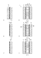
図1は、本発明の光学デバイスの一実施形態の断面を模式的に示したものであり、図2は、本発明の光学デバイスの一実施形態の断面について、基板と隔壁との界面を拡大して模式的に示したものである。また、図3は、本発明の光学デバイスの製造方法の一実施形態について、製造工程の流れの一例を示したものである。
なお、図1〜図3の中で開示した各部材については、説明の便宜のため、実際とは異なる縮尺及び形状で表しているものもある。
まず、本発明の光学デバイスの一実施形態について説明する。
本発明の一実施形態に係る光学デバイスは、図1に示すように、対向して配設された基板10と、該基板10の対向面内に形成された、隣接する空間を区切る隔壁20と、該隔壁20によって区切られた空間内に充填された、電界制御材料を含む流動体30と、を備える光学デバイス1である。
そして、本発明の一実施形態に係る光学デバイス1は、図1に示すように、少なくとも一方(図1では両方)の前記基板10と前記隔壁20との間に、微細な凹凸形状を有する微細凹凸層40及び該微細凹凸層40の形状に倣って形成された導電層50を、さらに備えることを特徴とする。
(基板)
本発明の一実施形態に係る光学デバイス1は、図1に示すように、対向するように設けられた基板10を備える。
ここで、前記基板10は、透明基板であり、それぞれ対向する面とは反対の面10aに電極(図示せず)を有する。
なお、本明細書において「透明」とは、可視光帯域(おおよそ360nm〜830nm)に属する波長の光の透過率が高いことを意味し、例えば、当該光の透過率が70%以上であることを意味する。
前記基板10の材料として、例えば、ポリエチレン(PE)、ポリエチレンテレフタレート(PET)、ポリエーテルサルホン(PES)、ポリエチレンナフタレート(PEN)、ポリプロピレン(PP)、ポリカーボネート(PC)、シクロオレフィンポリマー、シクロオレフィンコポリマー、ポリイミド、塩化ビニル等の透明フィルムや、透明ガラス等の樹脂板が用いられる。
ここで、強度を確保しつつ、薄膜化を図る観点からは、前記基板10の厚さは、25〜200μmであることが好ましく、50〜150μmであることがより好ましい。
また、本発明の一実施形態に係る光学デバイス1は、図1に示すように、前記基板10の対向面内に形成された、隣接する空間を区切る隔壁20をさらに備える。
ここで、前記隔壁20の「隣接する空間を区切る」とは、隔壁によって前記基板10の対向面内に存在する空間を区切ることを意味している。例えば、図1では、隔壁20のうち、2つの基板10を結ぶ方向に延在する部分20aが、隣接する空間を区切っており、後述する流動体30を充填するための空間20b(「セル」とも呼ばれる)を形成している。
なお、前記隔壁によって区切られる空間20bの形状(パターン)についても、特に限定はされず、光学デバイス1の種類や要求される性能に応じて、適宜選択することができる。
また、本発明の一実施形態に係る光学デバイス1は、図1に示すように、前記隔壁20によって区切られた空間20b充填された流動体30をさらに備える。
ここで、前記流動体30は、電界制御材料(図示せず)を含み、該電界制御材料が前記基板10間に電界をかけた際に移動することによって、画像表示を行うことができる。
そして、本発明の光学デバイス1は、図1及び図2に示すように、少なくとも一方の前記基板10と前記隔壁20との間に、微細な凹凸形状を有する微細凹凸層40及び該微細凹凸層40の形状に倣って形成された導電層50をさらに備える。
前記微細凹凸層40及び前記導電層50が微細な凹凸形状を有することで、これらの層が反射防止構造体として働くことができる結果、光学デバイス1の光学性能を高めることができ、さらに、前記微細凹凸層40及び前記導電層50の微細な凹凸形状によって、アンカー効果が得られるため、前記基板10と前記隔壁20との間の密着性についても向上させることができる。加えて、前記微細凹凸層40については、フォトリソグラフィ等の煩雑なプロセスによって形成する必要はなく、インプリント等の効率的なプロセスによって形成できるため、光学デバイス1の製造効率の低下招くこともない。
前記微細凹凸層40を構成する材料については、特に限定はされないが、光の透過性及び密着性をより高めることができる観点から、光学部品用途に使用される、アクリルモノマー、アクリルオリゴマー等のアクリル樹脂、又は、エポキシ樹脂などを含有することが好ましい。
ここで、前記微細凹凸層40の凹凸の平均間隔Pは、隣り合う凸部間及び凹部間の間隔の算術平均値である。なお、前記微細凹凸層40の凹凸の平均間隔Pは、例えば、走査型電子顕微鏡(SEM)、あるいは断面透過型電子顕微鏡(断面TEM)などによって観察可能である。隣り合う凸部間及び凹部間の距離の算術平均値を導出する方法としては、例えば、隣り合う凸部の組み合わせ、及び/又は、隣り合う凹部の組み合わせをそれぞれ複数個ピックアップし、各組み合わせを構成する凸部間の距離および凹部間の距離を測定し、測定値を平均する方法が挙げられる。
なお、前記微細凹凸層40の凹凸の高低差Hは、例えば、走査型電子顕微鏡(SEM)、あるいは断面透過型電子顕微鏡(断面TEM)などによって観察可能である。凹凸の高低差Hの算術平均値を導出する方法としては、例えば、前記微細凹凸層40の凹凸の高低差Hを複数個計測し、それらの測定値を平均する方法が挙げられる。
前記微細凹凸層40をインプリントによって形成する条件については、特に限定されず、公知のインプリント装置を用いて行うことができる。例えば、前記微細凹凸層40の材料として紫外線硬化樹脂を用いる場合、フィルムの巻出し及び巻取り機構を有する円筒状モールド型と、該モールド型に当接する調圧可能なニップロールと、を用い、紫外線硬化樹脂を円筒状モールドに押しあてながら、紫外線硬化を行った後、フィルムを巻き取ることによって、微細凹凸層40を形成できる。
また、前記微細凹凸層40及び前記導電層50については、少なくとも一方の前記基板10と前記隔壁20との間に形成してもよいが、より密着性および光透過特性を向上させるためには、図1に示すように、両方の前記基板10と前記隔壁20との間に形成されることが好ましい。
本発明の光学デバイスの一実施形態では、上述した基板10、隔壁20、流動体30、微細凹凸層40及び導電層50の他にも、光学デバイスに要求される性能に応じて、その他の部材をさらに備えることもできる。
例えば、前記基板10の対向面とは反対の面10aに、ハードコート層、防曇層、粘着層、遮光層などが挙げられる。
次に、本発明の光学デバイスの製造方法の一実施形態について説明する。
本発明の一実施形態に係る光学デバイスの製造方法は、図3に示すように、2つの対向する基板10の対向面上に、微細凹凸層40を形成する工程(図3(a))と、前記微細凹凸層40を覆うように導電層50を形成する工程(図3(b))と、前記導電層50上に、隣接する空間を区切る隔壁構造21をインプリントによって形成する工程(図3(c)、(d))と、前記隔壁20の区切られた空間20b内に、電界制御材料を含む流動体30を充填する工程(図3(e)、(f))と、を備えることを特徴とする。
上記工程を経ることで、製造効率の低下を招くことなく、基板10と隔壁20との間の密着性を向上できるとともに、光学性能に優れた光学デバイス1を得ることができる。
前記微細凹凸層40をインプリントによって形成する条件については、特に限定されず、公知のインプリント装置を用いて行うことができる。例えば、前記微細凹凸層40の材料として紫外線硬化樹脂を用いる場合、フィルムの巻出し及び巻取り機構を有する円筒状モールド型と、該モールド型に当接する調圧可能なニップロールと、を用い、紫外線硬化樹脂を円筒状モールドに押しあてながら、紫外線硬化を行った後、フィルムを巻き取ることによって、微細凹凸層40を形成できる。
本発明の電子機器は、上述した本発明の光学デバイス1を有することを特徴とする。
本発明の電子機器は、基板と隔壁との間の密着性、及び、光学性能に優れた本発明の光学デバイス1を有するため、光学デバイスの耐久性が向上し、優れた光学性能を実現できる。
図1に示されるような、対向して配設された基板10と、該基板10の対向面上に形成された、微細凹凸層40と、該微細凹凸層40を覆うように形成された導電層50と、導電層の対向する面内に形成された隔壁20と、該隔壁20によって区切られた空間内に充填された、電界制御材料を含む流動体30と、を備えた光学デバイス1のサンプルを作製した。
(1)基板
ポリエーテルテレフタレートからなる基板を2枚用意した。
(2)微細凹凸層
微細凹凸層は、アクリル系の紫外線硬化性樹脂を材料として用い、インプリントプロセスにより形成した。アクリル系紫外線硬化樹脂については、以下の配合比の樹脂組成物から作製した。インプリントは、円筒状(直径150mm)の石英母材に対して、凹凸がフォトリソグラフィにより施されたモールドを用い、シート状の樹脂組成物に凹凸形状を施すとともに、紫外線を照射し、硬化させた。
モノマー(東亞合成「アロニックスM305」):45質量%
オリゴマー(日本合成化学「UV-1700」):20質量%
反応性希釈剤(KJ ケミカル「DMAA」):30質量%
光重合開始剤(BASFジャパン「イルガキュア184」):5質量%
また、作製した微細凹凸層の、凹凸の平均間隔P及び凹凸の平均高低差については、表1に示す条件とした。なお、比較例1のサンプルについては、微細凹凸層を形成していない。
(3)導電層
酸化インジウムスズ(スズ5%)の導電層をスパッタリングプロセスにより形成した。導電層の平均厚さは60nm、シート抵抗は150Ω/□である。
(4)隔壁
隔壁は、アクリル系の紫外線硬化性樹脂を材料として用い、インプリントプロセスにより形成した。アクリル系紫外線硬化樹脂については、以下の配合比の樹脂組成物から作製した。インプリントは、円筒状(直径150mm)の金属母材に対して、凹凸が切削加工により施されたモールドを用い、シート状の樹脂組成物に凹凸形状を施すとともに、紫外線を照射し、硬化させた。
モノマー(東亞合成「アロニックスM305」):30質量%
オリゴマー(日本合成化学「UV-1700」):30質量%
反応性希釈剤(KJ ケミカル「DMAA」):30質量%
光重合開始剤(BASFジャパン「イルガキュア184」):5質量%
また、作製した隔壁20は、図1に示すように、基板10同士をつなぐ方向に延在し、延在する部分20aの、形成ピッチが100μm、厚さが30μm、長さが70μmである。
(5)流動体
流動体については、電界制御材料(ナノカーボン材料)を有機溶媒(シクロヘキサン)に分散させた溶液を用い、スキージにより隔壁の区切られた空間内へ充填した。
(評価)
作製した光学デバイスの各サンプルについて、以下の評価(1)〜(5)を実施し、評価結果を表1に示す。
光学デバイスの各サンプルの作製において、微細凹凸層をインプリントによって形成した際の、モールドの離型が良好に行われたか否かについて、以下の基準に従って評価した。
○:モールドの離型を良好に行えた
△:微細凹凸層の一部で離型不良発生することがあった
×:離型不良が発生して微細凹凸層の形成が困難であった
得られた光学デバイスの各サンプルについて、JIS K 5400(1990年)に準拠した鉛筆引っ掻き試験を実施し、試験後の基板と隔壁との間の剥がれの有無を確認し、剥がれなかったマスの割合(%)を算出し、以下の基準に従って評価した。
〇:90%以上
△:10%以上〜90%未満
×:1%未満
得られた光学デバイスの各サンプルについて、測定装置(日本分光(株)V-570)によって、視感透過率(%)を測定し、以下の基準に従って評価した。
〇:70%以上
△:60%以上〜70%未満
×:60%未満
さらに、得られた光学デバイスの各サンプルについて、波長に対する視感透過率(%)の値をグラフにしたものを図5に示す。
得られた光学デバイスの各サンプルについて、暗室にて斜め(光学デバイスの表面に対して30°程度の角度)より白色光を照射し、回折光の有無を目視で確認し、以下の基準に従って評価した。
〇:ほとんど回折光は視認されなかった
△:回折光は視認できるが、強い回折光は視認されなかった
×:強い回折光が視認された
上述した評価(1)〜(4)の結果を踏まえて、以下の基準で総合評価を行った。
○:評価(1)〜(4)において、全ての評価結果が○であった
△:評価(1)〜(4)において、評価結果が△のものがあるが、×はなかった
×:評価(1)〜(4)において、評価結果が×のものがあった

一方、微細凹凸層を設けていない比較例の光学デバイスのサンプルについては、光の透過性や基板と隔壁との密着性の点で、不良な結果を示すことがわかった。
10 基板
10a 対向する面とは反対の面
20 隔壁
20a 2つの基板を結ぶ方向に延在する部分
20b 隔壁によって区切られた空間
21 隔壁構造
30 流動体
40 微細凹凸層
50 導電層
Claims (7)
- 対向して配設された基板と、該基板の対向面内に形成された、隣接する空間を区切る隔壁と、該隔壁によって区切られた空間内に充填された、電界制御材料を含む流動体と、を備える光学デバイスであって、
少なくとも一方の前記基板と前記隔壁との間に、微細な凹凸形状を有する微細凹凸層及び該微細凹凸層の形状に倣って形成された導電層を、さらに備えることを特徴とする、光学デバイス。 - 前記微細凹凸層の凹凸の平均間隔が、50〜300nmであることを特徴とする、請求項1に記載の光学デバイス。
- 前記微細凹凸層の凹凸の平均高低差が、30nm以上であることを特徴とする、請求項1又は2に記載の光学デバイス。
- 前記微細凹凸層の凹凸形状が、インプリントによって形成されることを特徴とする、請求項1〜3のいずれか1項に記載の光学デバイス。
- 前記微細凹凸層及び前記導電層は、両方の前記基板と前記隔壁との間に形成されていることを特徴とする、請求項1〜4のいずれか1項に記載の光学デバイス。
- 2つの対向する基板の対向面上に、微細凹凸層を形成する工程と、
前記微細凹凸層を覆うように導電層を形成する工程と、
前記導電層上に、隣接する空間を区切る隔壁構造をインプリントによって形成する工程と、
前記隔壁の区切られた空間内に、電界制御材料を含む流動体を充填する工程と、を備えることを特徴とする、光学デバイスの製造方法。 - 請求項1〜5のいずれか1項に記載の光学デバイスを有することを特徴とする、電子機器。
Priority Applications (3)
| Application Number | Priority Date | Filing Date | Title |
|---|---|---|---|
| JP2019108544A JP2020201401A (ja) | 2019-06-11 | 2019-06-11 | 光学デバイス、光学デバイスの製造方法及び電子機器 |
| US16/892,284 US11874436B2 (en) | 2019-06-11 | 2020-06-04 | Optical device having fluid-filled partitioned spaces with electric field control material |
| JP2023132350A JP7646758B2 (ja) | 2019-06-11 | 2023-08-15 | 光学デバイス、光学デバイスの製造方法及び電子機器 |
Applications Claiming Priority (1)
| Application Number | Priority Date | Filing Date | Title |
|---|---|---|---|
| JP2019108544A JP2020201401A (ja) | 2019-06-11 | 2019-06-11 | 光学デバイス、光学デバイスの製造方法及び電子機器 |
Related Child Applications (1)
| Application Number | Title | Priority Date | Filing Date |
|---|---|---|---|
| JP2023132350A Division JP7646758B2 (ja) | 2019-06-11 | 2023-08-15 | 光学デバイス、光学デバイスの製造方法及び電子機器 |
Publications (1)
| Publication Number | Publication Date |
|---|---|
| JP2020201401A true JP2020201401A (ja) | 2020-12-17 |
Family
ID=73743616
Family Applications (2)
| Application Number | Title | Priority Date | Filing Date |
|---|---|---|---|
| JP2019108544A Pending JP2020201401A (ja) | 2019-06-11 | 2019-06-11 | 光学デバイス、光学デバイスの製造方法及び電子機器 |
| JP2023132350A Active JP7646758B2 (ja) | 2019-06-11 | 2023-08-15 | 光学デバイス、光学デバイスの製造方法及び電子機器 |
Family Applications After (1)
| Application Number | Title | Priority Date | Filing Date |
|---|---|---|---|
| JP2023132350A Active JP7646758B2 (ja) | 2019-06-11 | 2023-08-15 | 光学デバイス、光学デバイスの製造方法及び電子機器 |
Country Status (2)
| Country | Link |
|---|---|
| US (1) | US11874436B2 (ja) |
| JP (2) | JP2020201401A (ja) |
Citations (6)
| Publication number | Priority date | Publication date | Assignee | Title |
|---|---|---|---|---|
| US20070046623A1 (en) * | 2005-08-26 | 2007-03-01 | Lg Electronics Inc. | Electronic paper display device, manufacturing method and driving method thereof |
| JP2012123086A (ja) * | 2010-12-07 | 2012-06-28 | Sony Corp | 導電性光学素子ならびに情報入力装置および表示装置 |
| JP2012203342A (ja) * | 2011-03-28 | 2012-10-22 | Sony Corp | 電気泳動素子、表示装置および電子機器 |
| KR20140036791A (ko) * | 2012-09-18 | 2014-03-26 | 한국전자통신연구원 | 전자종이 디스플레이 장치 및 그 제조 방법 |
| KR20150055927A (ko) * | 2013-11-14 | 2015-05-22 | 한국전자통신연구원 | 컬러 전자종이 디스플레이 및 그 색 구현 방법 |
| JP2015114448A (ja) * | 2013-12-11 | 2015-06-22 | セイコーエプソン株式会社 | 電気泳動表示装置、電気泳動表示装置の製造方法、電子機器 |
Family Cites Families (5)
| Publication number | Priority date | Publication date | Assignee | Title |
|---|---|---|---|---|
| WO2008069162A1 (en) * | 2006-12-05 | 2008-06-12 | Semiconductor Energy Laboratory Co., Ltd. | Anti-reflection film and display device |
| JP2015054402A (ja) | 2013-09-10 | 2015-03-23 | 三菱レイヨン株式会社 | 積層構造体およびその製造方法、反射防止物品 |
| EP3465337A4 (en) * | 2016-05-23 | 2019-12-25 | Clearink Displays, Inc. | HYBRID REFLECTIVE EMISSIVE IMAGE DISPLAY |
| JP2018185495A (ja) | 2017-04-27 | 2018-11-22 | 大日本印刷株式会社 | 表示装置 |
| EP4485061A3 (en) * | 2018-07-03 | 2025-04-16 | Wuxi CLEARink Limited | Color filter arrays for tir-based image displays |
-
2019
- 2019-06-11 JP JP2019108544A patent/JP2020201401A/ja active Pending
-
2020
- 2020-06-04 US US16/892,284 patent/US11874436B2/en active Active
-
2023
- 2023-08-15 JP JP2023132350A patent/JP7646758B2/ja active Active
Patent Citations (6)
| Publication number | Priority date | Publication date | Assignee | Title |
|---|---|---|---|---|
| US20070046623A1 (en) * | 2005-08-26 | 2007-03-01 | Lg Electronics Inc. | Electronic paper display device, manufacturing method and driving method thereof |
| JP2012123086A (ja) * | 2010-12-07 | 2012-06-28 | Sony Corp | 導電性光学素子ならびに情報入力装置および表示装置 |
| JP2012203342A (ja) * | 2011-03-28 | 2012-10-22 | Sony Corp | 電気泳動素子、表示装置および電子機器 |
| KR20140036791A (ko) * | 2012-09-18 | 2014-03-26 | 한국전자통신연구원 | 전자종이 디스플레이 장치 및 그 제조 방법 |
| KR20150055927A (ko) * | 2013-11-14 | 2015-05-22 | 한국전자통신연구원 | 컬러 전자종이 디스플레이 및 그 색 구현 방법 |
| JP2015114448A (ja) * | 2013-12-11 | 2015-06-22 | セイコーエプソン株式会社 | 電気泳動表示装置、電気泳動表示装置の製造方法、電子機器 |
Also Published As
| Publication number | Publication date |
|---|---|
| US11874436B2 (en) | 2024-01-16 |
| JP2023155286A (ja) | 2023-10-20 |
| JP7646758B2 (ja) | 2025-03-17 |
| US20200393598A1 (en) | 2020-12-17 |
Similar Documents
| Publication | Publication Date | Title |
|---|---|---|
| US8531406B2 (en) | Transparent conductive film, electrode sheet for use in touch panel, and touch panel | |
| JP5895677B2 (ja) | 表示シート、表示シートの製造方法、表示装置および電子機器 | |
| KR101555411B1 (ko) | 투명 도전성 필름 및 그 용도 | |
| CN106782772A (zh) | 透明导电薄膜 | |
| JP6044108B2 (ja) | 表示シート、表示シートの製造方法、表示装置および電子機器 | |
| CN102265354A (zh) | 透明导电性层叠体和使用其的透明触摸面板 | |
| US20150015934A1 (en) | Electrophoretic apparatus, manufacturing method of electrophoretic apparatus, and electronic apparatus | |
| JP5862136B2 (ja) | 電気泳動表示装置 | |
| US20160139479A1 (en) | Display unit and electronic apparatus | |
| JP2011154202A (ja) | 電気泳動表示媒体及びその製造方法 | |
| WO2012008230A1 (ja) | 電子ペーパー用カラーフィルタ部材、電子ペーパー、およびそれらの製造方法 | |
| JP7646758B2 (ja) | 光学デバイス、光学デバイスの製造方法及び電子機器 | |
| CN110612477A (zh) | 分隔壁图案膜及其制造方法 | |
| KR20140007221A (ko) | 은 나노와이어 시인성이 개선된 광학 필름 | |
| JP6221435B2 (ja) | 電気泳動装置、電気泳動装置の製造方法、及び電子機器 | |
| JP6123168B2 (ja) | 表示シート、表示シートの製造方法、表示装置および電子機器 | |
| KR102960764B1 (ko) | 캡슐화 전기영동 매체의 패턴화된 영역들을 포함하는 디스플레이 재료 | |
| US20260036863A1 (en) | Display material including patterned areas of encapsulated electrophoretic media | |
| JP2013068903A (ja) | 電気泳動表示装置 | |
| TWI815316B (zh) | 製造用於電泳顯示器之積層體之方法 | |
| EP3729190B1 (en) | Electrophoretic display device and electronic apparatus | |
| KR102396509B1 (ko) | 블랙 격벽 패턴 필름 및 이의 제조방법 | |
| JP4373997B2 (ja) | 透明導電膜形成用組成物、透明導電膜及びディスプレイ | |
| CN206292766U (zh) | 透明导电薄膜 | |
| TW202210300A (zh) | 聚合物薄膜 |
Legal Events
| Date | Code | Title | Description |
|---|---|---|---|
| A621 | Written request for application examination |
Free format text: JAPANESE INTERMEDIATE CODE: A621 Effective date: 20220513 |
|
| A977 | Report on retrieval |
Free format text: JAPANESE INTERMEDIATE CODE: A971007 Effective date: 20221213 |
|
| A131 | Notification of reasons for refusal |
Free format text: JAPANESE INTERMEDIATE CODE: A131 Effective date: 20221220 |
|
| A601 | Written request for extension of time |
Free format text: JAPANESE INTERMEDIATE CODE: A601 Effective date: 20230214 |
|
| A521 | Request for written amendment filed |
Free format text: JAPANESE INTERMEDIATE CODE: A523 Effective date: 20230418 |
|
| A02 | Decision of refusal |
Free format text: JAPANESE INTERMEDIATE CODE: A02 Effective date: 20230516 |