JP2020202003A - フェイルビット数計数回路及び不揮発性半導体記憶装置 - Google Patents
フェイルビット数計数回路及び不揮発性半導体記憶装置 Download PDFInfo
- Publication number
- JP2020202003A JP2020202003A JP2019109833A JP2019109833A JP2020202003A JP 2020202003 A JP2020202003 A JP 2020202003A JP 2019109833 A JP2019109833 A JP 2019109833A JP 2019109833 A JP2019109833 A JP 2019109833A JP 2020202003 A JP2020202003 A JP 2020202003A
- Authority
- JP
- Japan
- Prior art keywords
- circuit
- data
- fail
- page buffer
- counting
- Prior art date
- Legal status (The legal status is an assumption and is not a legal conclusion. Google has not performed a legal analysis and makes no representation as to the accuracy of the status listed.)
- Granted
Links
Images






Classifications
-
- H—ELECTRICITY
- H03—ELECTRONIC CIRCUITRY
- H03K—PULSE TECHNIQUE
- H03K23/00—Pulse counters comprising counting chains; Frequency dividers comprising counting chains
- H03K23/40—Gating or clocking signals applied to all stages, i.e. synchronous counters
-
- G—PHYSICS
- G11—INFORMATION STORAGE
- G11C—STATIC STORES
- G11C16/00—Erasable programmable read-only memories
- G11C16/02—Erasable programmable read-only memories electrically programmable
- G11C16/06—Auxiliary circuits, e.g. for writing into memory
- G11C16/34—Determination of programming status, e.g. threshold voltage, overprogramming or underprogramming, retention
-
- G—PHYSICS
- G11—INFORMATION STORAGE
- G11C—STATIC STORES
- G11C29/00—Checking stores for correct operation ; Subsequent repair; Testing stores during standby or offline operation
- G11C29/04—Detection or location of defective memory elements, e.g. cell constructio details, timing of test signals
- G11C29/08—Functional testing, e.g. testing during refresh, power-on self testing [POST] or distributed testing
- G11C29/12—Built-in arrangements for testing, e.g. built-in self testing [BIST] or interconnection details
- G11C29/38—Response verification devices
- G11C29/42—Response verification devices using error correcting codes [ECC] or parity check
-
- G—PHYSICS
- G11—INFORMATION STORAGE
- G11C—STATIC STORES
- G11C16/00—Erasable programmable read-only memories
- G11C16/02—Erasable programmable read-only memories electrically programmable
- G11C16/06—Auxiliary circuits, e.g. for writing into memory
- G11C16/30—Power supply circuits
-
- G—PHYSICS
- G11—INFORMATION STORAGE
- G11C—STATIC STORES
- G11C16/00—Erasable programmable read-only memories
- G11C16/02—Erasable programmable read-only memories electrically programmable
- G11C16/06—Auxiliary circuits, e.g. for writing into memory
- G11C16/32—Timing circuits
-
- G—PHYSICS
- G11—INFORMATION STORAGE
- G11C—STATIC STORES
- G11C29/00—Checking stores for correct operation ; Subsequent repair; Testing stores during standby or offline operation
- G11C29/04—Detection or location of defective memory elements, e.g. cell constructio details, timing of test signals
-
- G—PHYSICS
- G11—INFORMATION STORAGE
- G11C—STATIC STORES
- G11C29/00—Checking stores for correct operation ; Subsequent repair; Testing stores during standby or offline operation
- G11C29/04—Detection or location of defective memory elements, e.g. cell constructio details, timing of test signals
- G11C29/08—Functional testing, e.g. testing during refresh, power-on self testing [POST] or distributed testing
- G11C29/12—Built-in arrangements for testing, e.g. built-in self testing [BIST] or interconnection details
- G11C29/12015—Built-in arrangements for testing, e.g. built-in self testing [BIST] or interconnection details comprising clock generation or timing circuitry
-
- G—PHYSICS
- G11—INFORMATION STORAGE
- G11C—STATIC STORES
- G11C29/00—Checking stores for correct operation ; Subsequent repair; Testing stores during standby or offline operation
- G11C29/04—Detection or location of defective memory elements, e.g. cell constructio details, timing of test signals
- G11C29/08—Functional testing, e.g. testing during refresh, power-on self testing [POST] or distributed testing
- G11C29/12—Built-in arrangements for testing, e.g. built-in self testing [BIST] or interconnection details
- G11C29/18—Address generation devices; Devices for accessing memories, e.g. details of addressing circuits
- G11C29/20—Address generation devices; Devices for accessing memories, e.g. details of addressing circuits using counters or linear-feedback shift registers [LFSR]
-
- G—PHYSICS
- G11—INFORMATION STORAGE
- G11C—STATIC STORES
- G11C29/00—Checking stores for correct operation ; Subsequent repair; Testing stores during standby or offline operation
- G11C29/04—Detection or location of defective memory elements, e.g. cell constructio details, timing of test signals
- G11C29/08—Functional testing, e.g. testing during refresh, power-on self testing [POST] or distributed testing
- G11C29/12—Built-in arrangements for testing, e.g. built-in self testing [BIST] or interconnection details
- G11C29/44—Indication or identification of errors, e.g. for repair
-
- G—PHYSICS
- G11—INFORMATION STORAGE
- G11C—STATIC STORES
- G11C7/00—Arrangements for writing information into, or reading information out from, a digital store
- G11C7/10—Input/output [I/O] data interface arrangements, e.g. I/O data control circuits, I/O data buffers
- G11C7/1006—Data managing, e.g. manipulating data before writing or reading out, data bus switches or control circuits therefor
-
- G—PHYSICS
- G11—INFORMATION STORAGE
- G11C—STATIC STORES
- G11C7/00—Arrangements for writing information into, or reading information out from, a digital store
- G11C7/10—Input/output [I/O] data interface arrangements, e.g. I/O data control circuits, I/O data buffers
- G11C7/1051—Data output circuits, e.g. read-out amplifiers, data output buffers, data output registers, data output level conversion circuits
- G11C7/1057—Data output buffers, e.g. comprising level conversion circuits, circuits for adapting load
-
- G—PHYSICS
- G11—INFORMATION STORAGE
- G11C—STATIC STORES
- G11C7/00—Arrangements for writing information into, or reading information out from, a digital store
- G11C7/10—Input/output [I/O] data interface arrangements, e.g. I/O data control circuits, I/O data buffers
- G11C7/1078—Data input circuits, e.g. write amplifiers, data input buffers, data input registers, data input level conversion circuits
- G11C7/1084—Data input buffers, e.g. comprising level conversion circuits, circuits for adapting load
-
- G—PHYSICS
- G11—INFORMATION STORAGE
- G11C—STATIC STORES
- G11C16/00—Erasable programmable read-only memories
- G11C16/02—Erasable programmable read-only memories electrically programmable
- G11C16/04—Erasable programmable read-only memories electrically programmable using variable threshold transistors, e.g. FAMOS
- G11C16/0483—Erasable programmable read-only memories electrically programmable using variable threshold transistors, e.g. FAMOS comprising cells having several storage transistors connected in series
-
- G—PHYSICS
- G11—INFORMATION STORAGE
- G11C—STATIC STORES
- G11C16/00—Erasable programmable read-only memories
- G11C16/02—Erasable programmable read-only memories electrically programmable
- G11C16/06—Auxiliary circuits, e.g. for writing into memory
- G11C16/10—Programming or data input circuits
-
- G—PHYSICS
- G11—INFORMATION STORAGE
- G11C—STATIC STORES
- G11C16/00—Erasable programmable read-only memories
- G11C16/02—Erasable programmable read-only memories electrically programmable
- G11C16/06—Auxiliary circuits, e.g. for writing into memory
- G11C16/26—Sensing or reading circuits; Data output circuits
-
- G—PHYSICS
- G11—INFORMATION STORAGE
- G11C—STATIC STORES
- G11C29/00—Checking stores for correct operation ; Subsequent repair; Testing stores during standby or offline operation
- G11C29/04—Detection or location of defective memory elements, e.g. cell constructio details, timing of test signals
- G11C29/08—Functional testing, e.g. testing during refresh, power-on self testing [POST] or distributed testing
- G11C29/12—Built-in arrangements for testing, e.g. built-in self testing [BIST] or interconnection details
- G11C2029/1204—Bit line control
Landscapes
- Read Only Memory (AREA)
- For Increasing The Reliability Of Semiconductor Memories (AREA)
Abstract
Description
複数のメモリセルからなる不揮発性のメモリセルアレイと、複数のセグメントからなるデータを上記メモリセルアレイに対してページバッファを介して書き込み及び上記メモリセルアレイから前記ページバッファを介して読み出しを制御し、書き込み又は読み出し時に発生するフェイルビット数を計数する制御回路とを備えた、不揮発性半導体記憶装置のためのフェイルビット数計数回路であって、
前記ページバッファは、パスビット又はフェイルビットを示すCRデータを出力する所定容量の複数のページバッファ部に分割され、
前記各ページバッファ部からのパスビットを示すCRデータに対してオンとなり、フェイルビットを示すCRデータに対してオフとなる複数のスイッチ素子を直列に接続して直列回路で構成されたデータ転送回路を備え、
前記制御回路は、前記データ転送回路の一方の入力端子に計数イネーブル信号を入力し、所定周期のクロックに応じて前記計数イネーブル信号を次段のオフの前記スイッチ素子まで前記直列回路を介して順次転送し、
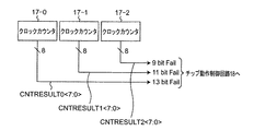
前記データ転送回路の一方の入力端子に計数イネーブル信号を入力した後、前記データ転送回路の他方の出力端子に前記計数イネーブル信号が到達するまでの前記クロックの数をフェイルビット数として計数するクロックカウンタを備えたことを特徴とする。
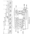
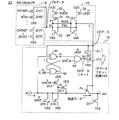
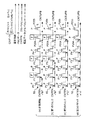
ここで、図8のデータ転送回路16の動作を以下の表1に示す。

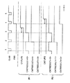
JDG<7:0>:CRデータを出力するロジック(制御)信号であり、当該信号の動作は1つのページバッファ毎行われ、対象のページバッファは1回の動作で1つのみである。
RDEN:PBデータをCRデータラッチ15に取り込む信号であり、基本的には、JDG<7:0>信号の論理和のロジックで生成される。
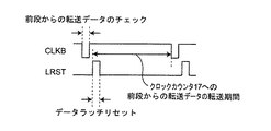
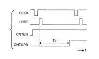
LRST:ラッチリセット時と、前段の転送データJDn−1をラッチ(N1,N2による)に取り込むときに動作する信号である。
SRST,SRSTB:PチャネルMOSトランジスタPnのストリングをリセットするための信号である。
CLKB:ローイネーブルのクロックであり、フェイル数を計数するために用いる。
JDn−1:前段からの転送データである。
JDn:前段からの転送データ及び自段のCRデータに基づく転送データであり、初期状態と、パスビットのときは、JDn−1がそのままJDnになる。
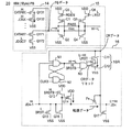
図15は変形例に係るページバッファ回路20Aの構成例を示す回路図である。図15のページバッファ回路20Aは、図8のページバッファ回路20に比較して、以下の点が異なる。
(1)CRデータラッチ15に代えて、CRデータ転送回路15Aを備えた。
(2)データ転送回路16に代えて、データ転送回路16Aを備えた。
以下、相違点について詳述する。
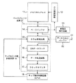
12 ロウ制御回路
13 高電圧発生回路
14 ページバッファ
15 CRデータラッチ
15A CRデータ転送回路
16,16A データ転送回路
16R CRデータリセット回路
17,17A,17−0〜17−2 クロックカウンタ
18 チップ動作制御回路
20 ページバッファ回路
21 入出力端子
22 データ入出力バッファ
30 カラム制御回路
201 ページバッファ
202 インバータ
203 電流源
INV1 インバータ
N1〜N3 ナンドゲート
Pn,P0〜P255 PチャネルMOSトランジスタ
Q1〜Q172,Q201〜Q206 MOSトランジスタ
T1 検出点
Claims (8)
- 複数のメモリセルからなる不揮発性のメモリセルアレイと、複数のセグメントからなるデータを上記メモリセルアレイに対してページバッファを介して書き込み及び上記メモリセルアレイから前記ページバッファを介して読み出しを制御し、書き込み又は読み出し時に発生するフェイルビット数を計数する制御回路とを備えた、不揮発性半導体記憶装置のためのフェイルビット数計数回路であって、
前記ページバッファは、パスビット又はフェイルビットを示す計算結果データを出力する所定容量の複数のページバッファ部に分割され、
前記各ページバッファ部からのパスビットを示す計算結果データに対してオンとなり、フェイルビットを示す計算結果データに対してオフとなる複数のスイッチ素子を直列に接続して直列回路で構成されたデータ転送回路を備え、
前記制御回路は、前記データ転送回路の一方の入力端子に計数イネーブル信号を入力し、所定周期のクロックに応じて前記計数イネーブル信号を次段のオフの前記スイッチ素子まで前記直列回路を介して順次転送し、
前記データ転送回路の一方の入力端子に計数イネーブル信号を入力した後、前記データ転送回路の他方の出力端子に前記計数イネーブル信号が到達するまでの前記クロックの数をフェイルビット数として計数するクロックカウンタを備えたことを特徴とする、不揮発性半導体記憶装置のためのフェイルビット数計数回路。 - 前記クロックカウンタは、前記不揮発性半導体記憶装置のチップの動作を制御する演算回路に内蔵されることを特徴とする、請求項1記載のフェイルビット数計数回路。
- 前記データ転送回路は、前段のデータ転送回路からの転送データがフェイルビットのときでかつ前記計算結果データがフェイルビットを示すときに、前記ページバッファのデータに対応するデータを次段のデータ転送回路に送信することを特徴とする請求項1又は2記載のフェイルビット数計数回路。
- 前記各ページバッファ部からのパスビットを示す計算結果データを一時的にラッチした後、前記各スイッチ素子の制御端子に転送する計算結果データラッチをさらに備えたことを特徴とする請求項1〜3のうちのいずれか1つに記載のフェイルビット数計数回路。
- 複数のページバッファにそれぞれ対応する複数のクロックカウンタを備え、
前記制御回路は、前記複数のクロックカウンタからのフェイルビット数を加算することで、前記複数のページバッファの全体のフェイルビット数を計算することを特徴とする、請求項1〜4のうちのいずれか1つに記載のフェイルビット数計数回路。 - 前記各スイッチ素子は、PチャネルMOSトランジスタであることを特徴とする請求項1〜5のうちのいずれか1つに記載のフェイルビット数計数回路。
- 前記データ転送回路は、前記複数のスイッチ素子のオン抵抗の増大により伝送速度の低下が発生しないように、前記計算結果データを転送する前記直列回路に所定の電圧を印加する電源回路をさらに備えたことを特徴とする請求項1〜6のうちのいずれか1つに記載のフェイルビット数計数回路。
- 請求項1〜7のうちのいずれか1つに記載のフェイルビット数計数回路を備えたことを特徴とする不揮発性半導体記憶装置。
Priority Applications (4)
| Application Number | Priority Date | Filing Date | Title |
|---|---|---|---|
| JP2019109833A JP6757447B1 (ja) | 2019-06-12 | 2019-06-12 | フェイルビット数計数回路及び不揮発性半導体記憶装置 |
| US16/796,957 US11004522B2 (en) | 2019-06-12 | 2020-02-21 | Fail bit number counting circuit and non-volatile semiconductor storage device |
| TW109110853A TWI725799B (zh) | 2019-06-12 | 2020-03-30 | 失效位元數目計數電路及非揮發性半導體儲存裝置 |
| CN202010311415.6A CN112086123B (zh) | 2019-06-12 | 2020-04-20 | 失效位数目计数电路及非易失性半导体储存装置 |
Applications Claiming Priority (1)
| Application Number | Priority Date | Filing Date | Title |
|---|---|---|---|
| JP2019109833A JP6757447B1 (ja) | 2019-06-12 | 2019-06-12 | フェイルビット数計数回路及び不揮発性半導体記憶装置 |
Publications (2)
| Publication Number | Publication Date |
|---|---|
| JP6757447B1 JP6757447B1 (ja) | 2020-09-16 |
| JP2020202003A true JP2020202003A (ja) | 2020-12-17 |
Family
ID=72432308
Family Applications (1)
| Application Number | Title | Priority Date | Filing Date |
|---|---|---|---|
| JP2019109833A Active JP6757447B1 (ja) | 2019-06-12 | 2019-06-12 | フェイルビット数計数回路及び不揮発性半導体記憶装置 |
Country Status (4)
| Country | Link |
|---|---|
| US (1) | US11004522B2 (ja) |
| JP (1) | JP6757447B1 (ja) |
| CN (1) | CN112086123B (ja) |
| TW (1) | TWI725799B (ja) |
Families Citing this family (2)
| Publication number | Priority date | Publication date | Assignee | Title |
|---|---|---|---|---|
| US11513880B1 (en) * | 2021-08-26 | 2022-11-29 | Powerchip Semiconductor Manufacturing Corporation | Failure bit count circuit for memory and method thereof |
| KR20250139497A (ko) * | 2024-03-15 | 2025-09-23 | 삼성전자주식회사 | 페일 비트 카운트 동작 또는 포지션 서치 동작을 수행하는 스캔 레지스터 회로 및 그것을 포함하는 메모리 장치 |
Family Cites Families (18)
| Publication number | Priority date | Publication date | Assignee | Title |
|---|---|---|---|---|
| KR950000273B1 (ko) | 1992-02-21 | 1995-01-12 | 삼성전자 주식회사 | 불휘발성 반도체 메모리장치 및 그 최적화 기입방법 |
| JP2000285692A (ja) | 1999-04-01 | 2000-10-13 | Sony Corp | 不揮発性半導体記憶装置、並びにデータ書き込み方法およびデータ読み出し方法 |
| JP2001028575A (ja) | 1999-07-13 | 2001-01-30 | Victor Co Of Japan Ltd | デジタル放送受信装置 |
| JP4250325B2 (ja) | 2000-11-01 | 2009-04-08 | 株式会社東芝 | 半導体記憶装置 |
| KR100399365B1 (ko) | 2000-12-04 | 2003-09-26 | 삼성전자주식회사 | 페일 비트 검출 스킴을 구비한 불휘발성 반도체 메모리장치 및 그것의 페일 비트 카운트 방법 |
| JP2003346485A (ja) | 2002-05-23 | 2003-12-05 | Fujitsu Ltd | 不揮発性半導体記憶装置及び不揮発性半導体記憶装置の書き込み方法 |
| JP2006012367A (ja) * | 2004-06-29 | 2006-01-12 | Toshiba Corp | 不揮発性半導体記憶装置 |
| US7428180B2 (en) * | 2006-01-25 | 2008-09-23 | Samsung Electronics Co., Ltd. | Semiconductor memory devices and methods of testing for failed bits of semiconductor memory devices |
| KR100933859B1 (ko) * | 2007-11-29 | 2009-12-24 | 주식회사 하이닉스반도체 | 플래시 메모리 소자 및 그것의 프로그램 방법 |
| KR100965077B1 (ko) * | 2008-11-14 | 2010-06-21 | 주식회사 하이닉스반도체 | 불휘발성 메모리 장치의 페일 비트 카운터 |
| JP2012133840A (ja) * | 2010-12-20 | 2012-07-12 | Samsung Yokohama Research Institute Co Ltd | 半導体記憶装置、及び記憶方法 |
| JP2012203965A (ja) * | 2011-03-25 | 2012-10-22 | Toshiba Corp | 半導体記憶装置 |
| JP5678151B1 (ja) * | 2013-09-18 | 2015-02-25 | 力晶科技股▲ふん▼有限公司 | 不揮発性半導体記憶装置とその制御方法 |
| JP5909294B1 (ja) * | 2015-03-11 | 2016-04-26 | 力晶科技股▲ふん▼有限公司 | 不揮発性記憶装置のための書き込み回路及び方法、並びに不揮発性記憶装置 |
| JP6114796B1 (ja) * | 2015-10-05 | 2017-04-12 | 力晶科技股▲ふん▼有限公司 | 不揮発性記憶装置のためのセンス回路及び不揮発性記憶装置 |
| US10297337B2 (en) * | 2017-08-04 | 2019-05-21 | Sandisk Technologies Llc | Hierarchical fail bit counting circuit in memory device |
| KR20190032104A (ko) * | 2017-09-19 | 2019-03-27 | 에스케이하이닉스 주식회사 | 비휘발성 메모리 장치, 비휘발성 메모리 장치를 포함하는 데이터 저장 장치 및 그것의 동작 방법 |
| US10482986B2 (en) * | 2017-10-25 | 2019-11-19 | Western Digital Technologies, Inc. | Adaptive erase fail bit criteria |
-
2019
- 2019-06-12 JP JP2019109833A patent/JP6757447B1/ja active Active
-
2020
- 2020-02-21 US US16/796,957 patent/US11004522B2/en active Active
- 2020-03-30 TW TW109110853A patent/TWI725799B/zh active
- 2020-04-20 CN CN202010311415.6A patent/CN112086123B/zh active Active
Also Published As
| Publication number | Publication date |
|---|---|
| TWI725799B (zh) | 2021-04-21 |
| US11004522B2 (en) | 2021-05-11 |
| CN112086123A (zh) | 2020-12-15 |
| US20200395085A1 (en) | 2020-12-17 |
| JP6757447B1 (ja) | 2020-09-16 |
| TW202105401A (zh) | 2021-02-01 |
| CN112086123B (zh) | 2022-09-27 |
Similar Documents
| Publication | Publication Date | Title |
|---|---|---|
| JP3647996B2 (ja) | 不揮発性半導体メモリ装置とその読出及びプログラム方法 | |
| JP4566369B2 (ja) | 不揮発性半導体メモリ装置 | |
| CN107766171B (zh) | 与非型快闪存储器及其读出方法 | |
| US10481965B2 (en) | Method and apparatus for determining status element total with sequentially coupled counting status circuits | |
| US10748607B2 (en) | Non-volatile memory device and associated peripheral circuit with data verifying and rewriting functions | |
| JP2006012367A (ja) | 不揮発性半導体記憶装置 | |
| JPS63285800A (ja) | 半導体メモリ装置 | |
| JP6757447B1 (ja) | フェイルビット数計数回路及び不揮発性半導体記憶装置 | |
| JP4686350B2 (ja) | 不揮発性半導体記憶装置及びその自己テスト方法 | |
| CN101563675B (zh) | 具有高写入并行度的用于快闪存储器的列冗余 | |
| KR101092012B1 (ko) | 반도체 장치 및 써넣기 방법 | |
| JP4499111B2 (ja) | 不揮発性記憶装置の情報設定方法、および不揮発性記憶装置 | |
| CN104900269B (zh) | 半导体存储装置及其冗余方法 | |
| CN113674794B (zh) | 半导体存储装置以及错误检测纠正相关信息的读出方法 | |
| JPH11134884A (ja) | 半導体装置 | |
| JP2012128921A (ja) | 半導体記憶装置 | |
| US9852024B2 (en) | Apparatus and method for read time control in ECC-enabled flash memory | |
| KR100673776B1 (ko) | 플래시 메모리 장치의 페이지 버퍼 및 이를 이용한 데이터리드 방법 | |
| JP4074276B2 (ja) | 半導体装置 | |
| CN108399934B (zh) | 半导体存储装置及数据设定方法 | |
| CN101399074B (zh) | 集成电路中存储器电路及其控制方法 | |
| JP2009252290A (ja) | 半導体集積回路およびその動作方法 | |
| JP4530562B2 (ja) | 不揮発性メモリ | |
| KR19980042664A (ko) | 소거 기능의 테스트용 테스트 회로를 가진 비휘발성 반도체메모리 | |
| CN120126535A (zh) | 半导体器件 |
Legal Events
| Date | Code | Title | Description |
|---|---|---|---|
| A621 | Written request for application examination |
Free format text: JAPANESE INTERMEDIATE CODE: A621 Effective date: 20190612 |
|
| TRDD | Decision of grant or rejection written | ||
| A01 | Written decision to grant a patent or to grant a registration (utility model) |
Free format text: JAPANESE INTERMEDIATE CODE: A01 Effective date: 20200825 |
|
| A61 | First payment of annual fees (during grant procedure) |
Free format text: JAPANESE INTERMEDIATE CODE: A61 Effective date: 20200828 |
|
| R150 | Certificate of patent or registration of utility model |
Ref document number: 6757447 Country of ref document: JP Free format text: JAPANESE INTERMEDIATE CODE: R150 |
|
| R250 | Receipt of annual fees |
Free format text: JAPANESE INTERMEDIATE CODE: R250 |
|
| R250 | Receipt of annual fees |
Free format text: JAPANESE INTERMEDIATE CODE: R250 |
|
| R250 | Receipt of annual fees |
Free format text: JAPANESE INTERMEDIATE CODE: R250 |