JP2020519952A - スイッチャブル層および少なくとも1つの光学層を有する光学デバイス - Google Patents
スイッチャブル層および少なくとも1つの光学層を有する光学デバイス Download PDFInfo
- Publication number
- JP2020519952A JP2020519952A JP2019561906A JP2019561906A JP2020519952A JP 2020519952 A JP2020519952 A JP 2020519952A JP 2019561906 A JP2019561906 A JP 2019561906A JP 2019561906 A JP2019561906 A JP 2019561906A JP 2020519952 A JP2020519952 A JP 2020519952A
- Authority
- JP
- Japan
- Prior art keywords
- switchable
- layer
- optical device
- light
- reflection
- Prior art date
- Legal status (The legal status is an assumption and is not a legal conclusion. Google has not performed a legal analysis and makes no representation as to the accuracy of the status listed.)
- Granted
Links
Images



Classifications
-
- G—PHYSICS
- G02—OPTICS
- G02F—OPTICAL DEVICES OR ARRANGEMENTS FOR THE CONTROL OF LIGHT BY MODIFICATION OF THE OPTICAL PROPERTIES OF THE MEDIA OF THE ELEMENTS INVOLVED THEREIN; NON-LINEAR OPTICS; FREQUENCY-CHANGING OF LIGHT; OPTICAL LOGIC ELEMENTS; OPTICAL ANALOGUE/DIGITAL CONVERTERS
- G02F1/00—Devices or arrangements for the control of the intensity, colour, phase, polarisation or direction of light arriving from an independent light source, e.g. switching, gating or modulating; Non-linear optics
- G02F1/01—Devices or arrangements for the control of the intensity, colour, phase, polarisation or direction of light arriving from an independent light source, e.g. switching, gating or modulating; Non-linear optics for the control of the intensity, phase, polarisation or colour
- G02F1/13—Devices or arrangements for the control of the intensity, colour, phase, polarisation or direction of light arriving from an independent light source, e.g. switching, gating or modulating; Non-linear optics for the control of the intensity, phase, polarisation or colour based on liquid crystals, e.g. single liquid crystal display cells
- G02F1/137—Devices or arrangements for the control of the intensity, colour, phase, polarisation or direction of light arriving from an independent light source, e.g. switching, gating or modulating; Non-linear optics for the control of the intensity, phase, polarisation or colour based on liquid crystals, e.g. single liquid crystal display cells characterised by the electro-optical or magneto-optical effect, e.g. field-induced phase transition, orientation effect, guest-host interaction or dynamic scattering
- G02F1/13725—Devices or arrangements for the control of the intensity, colour, phase, polarisation or direction of light arriving from an independent light source, e.g. switching, gating or modulating; Non-linear optics for the control of the intensity, phase, polarisation or colour based on liquid crystals, e.g. single liquid crystal display cells characterised by the electro-optical or magneto-optical effect, e.g. field-induced phase transition, orientation effect, guest-host interaction or dynamic scattering based on guest-host interaction
-
- G—PHYSICS
- G02—OPTICS
- G02F—OPTICAL DEVICES OR ARRANGEMENTS FOR THE CONTROL OF LIGHT BY MODIFICATION OF THE OPTICAL PROPERTIES OF THE MEDIA OF THE ELEMENTS INVOLVED THEREIN; NON-LINEAR OPTICS; FREQUENCY-CHANGING OF LIGHT; OPTICAL LOGIC ELEMENTS; OPTICAL ANALOGUE/DIGITAL CONVERTERS
- G02F1/00—Devices or arrangements for the control of the intensity, colour, phase, polarisation or direction of light arriving from an independent light source, e.g. switching, gating or modulating; Non-linear optics
- G02F1/01—Devices or arrangements for the control of the intensity, colour, phase, polarisation or direction of light arriving from an independent light source, e.g. switching, gating or modulating; Non-linear optics for the control of the intensity, phase, polarisation or colour
- G02F1/13—Devices or arrangements for the control of the intensity, colour, phase, polarisation or direction of light arriving from an independent light source, e.g. switching, gating or modulating; Non-linear optics for the control of the intensity, phase, polarisation or colour based on liquid crystals, e.g. single liquid crystal display cells
- G02F1/133—Constructional arrangements; Operation of liquid crystal cells; Circuit arrangements
- G02F1/1333—Constructional arrangements; Manufacturing methods
- G02F1/1335—Structural association of cells with optical devices, e.g. polarisers or reflectors
- G02F1/133553—Reflecting elements
-
- G—PHYSICS
- G02—OPTICS
- G02F—OPTICAL DEVICES OR ARRANGEMENTS FOR THE CONTROL OF LIGHT BY MODIFICATION OF THE OPTICAL PROPERTIES OF THE MEDIA OF THE ELEMENTS INVOLVED THEREIN; NON-LINEAR OPTICS; FREQUENCY-CHANGING OF LIGHT; OPTICAL LOGIC ELEMENTS; OPTICAL ANALOGUE/DIGITAL CONVERTERS
- G02F1/00—Devices or arrangements for the control of the intensity, colour, phase, polarisation or direction of light arriving from an independent light source, e.g. switching, gating or modulating; Non-linear optics
- G02F1/01—Devices or arrangements for the control of the intensity, colour, phase, polarisation or direction of light arriving from an independent light source, e.g. switching, gating or modulating; Non-linear optics for the control of the intensity, phase, polarisation or colour
- G02F1/13—Devices or arrangements for the control of the intensity, colour, phase, polarisation or direction of light arriving from an independent light source, e.g. switching, gating or modulating; Non-linear optics for the control of the intensity, phase, polarisation or colour based on liquid crystals, e.g. single liquid crystal display cells
- G02F1/133—Constructional arrangements; Operation of liquid crystal cells; Circuit arrangements
- G02F1/1333—Constructional arrangements; Manufacturing methods
- G02F1/1335—Structural association of cells with optical devices, e.g. polarisers or reflectors
- G02F1/13363—Birefringent elements, e.g. for optical compensation
- G02F1/133638—Waveplates, i.e. plates with a retardation value of lambda/n
-
- G—PHYSICS
- G02—OPTICS
- G02F—OPTICAL DEVICES OR ARRANGEMENTS FOR THE CONTROL OF LIGHT BY MODIFICATION OF THE OPTICAL PROPERTIES OF THE MEDIA OF THE ELEMENTS INVOLVED THEREIN; NON-LINEAR OPTICS; FREQUENCY-CHANGING OF LIGHT; OPTICAL LOGIC ELEMENTS; OPTICAL ANALOGUE/DIGITAL CONVERTERS
- G02F1/00—Devices or arrangements for the control of the intensity, colour, phase, polarisation or direction of light arriving from an independent light source, e.g. switching, gating or modulating; Non-linear optics
- G02F1/01—Devices or arrangements for the control of the intensity, colour, phase, polarisation or direction of light arriving from an independent light source, e.g. switching, gating or modulating; Non-linear optics for the control of the intensity, phase, polarisation or colour
- G02F1/15—Devices or arrangements for the control of the intensity, colour, phase, polarisation or direction of light arriving from an independent light source, e.g. switching, gating or modulating; Non-linear optics for the control of the intensity, phase, polarisation or colour based on an electrochromic effect
- G02F1/153—Constructional details
- G02F1/155—Electrodes
Landscapes
- Physics & Mathematics (AREA)
- Nonlinear Science (AREA)
- General Physics & Mathematics (AREA)
- Optics & Photonics (AREA)
- Chemical & Material Sciences (AREA)
- Crystallography & Structural Chemistry (AREA)
- Mathematical Physics (AREA)
- Liquid Crystal (AREA)
- Polarising Elements (AREA)
- Mechanical Light Control Or Optical Switches (AREA)
Abstract
Description
C(λ)=(1−R(λ))×(ΤΒ(λ)−TD(λ)) (1)
と定義され、C(λ)は、波長λを有する光に対するコントラストであり、R(λ)(上記のように定義される反射強度)は、波長λを有する光に対する反射による損失強度であり、ΤΒ(λ)およびTD(λ)(上記のように定義される透過強度)は、それぞれ明状態および暗状態に対する、波長λを有する透過光の強度である。反射強度および透過強度は、0と1との間の無次元数として与えられる。反射損失には、スイッチャブル光学デバイスの少なくとも1つの光学層における反射も、別のすべての層における反射も含まれる。
n×d=λ/4
にしたがい、ただしnは、反射防止層の材料の屈折率、dは、反射防止層の厚さ、λは、最小反射率の波長である。
D=I1/I2
と定義され、ただしI1は、第1偏光の透過光の強度であり、I2は、第1偏光方向と直交する第2偏光の透過光の強度である。第1偏光は、透過強度が大きい方の偏光として定義される。好ましくは、ダイクロイックコントラストDは、スペクトルの可視範囲における光に対し、少なくとも2であり、さらに好ましくは少なくとも4であり、最も好ましくは少なくとも10である。
P=R1/R2
と定義され、ただしR1は、第1偏光の反射光の強度であり、R2は、第1偏光方向と直交する第2偏光方向の反射光の強度である。第1偏光は、反射強度が大きい方の偏光として定義される。好ましくは、偏光コントラストPは、少なくとも1つの反射帯域内の波長を有する光に対し、少なくとも2であり、さらに好ましくは少なくとも4であり、最も好ましくは少なくとも10である。
実施例1A
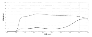
外側から緑色に見えるスイッチャブルウィンドウを製造するためには、2つのタイプのコーティングガラス基板が、主要ガラスサプライヤから入手される。第1基板の一方の面には、50%の反射強度を有する選択的反射コーティングがコーティングされている。他方の面には、透明導電性酸化物(TCO transparent conductive oxide)がコーティングされている。緑色に見えるようにするために、選択的反射コーティングは、約550nmの中心波長および約100nmの帯域幅を有するように指定される。第2基板は、一方の面にTCOコーティングを有し、かつ他方の面にコーティングを有しない。
表1

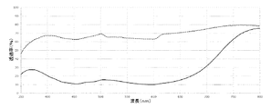
ここではデバイスは、染料がドーピングされた液晶混合物の吸収スペクトルが、選択的反射コーティングの反射スペクトルと相補的になるように調整される(すなわち可視スペクトルの青色および赤色部分においてより吸収される)点において実施例1Aのデバイスとは異なるように構成されている。この混合物の透過スペクトルは、図5に示されている。他のすべての面において、このデバイスは、実施例1Aのデバイスと同じである。
表2
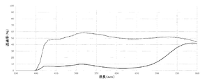
択一的な一実施例として、反射層が、上記の実施例1Aおよび1Bのように50%ではなく10%の反射強度を有するようにスイッチャブルデバイスを構成可能である。この場合、比較実施例(2A)は、実施例1Aのように50%ではなく10%である、反射層の反射強度を除いて、すべての面において実施例1Aと同一である。実施例2Aに対し、図7に示した透過スペクトルが得られる(破線=明状態;実線=暗状態)。このデバイスは、表3に示したCRI座標からわかるように暗状態において着色している。すなわち、
表3
表4
表5
Claims (16)
- 少なくとも1つのスイッチャブル層(15)と、少なくとも1つの光学層(20、22)とを含む層構造を有するスイッチャブル光学デバイス(10)であって、
少なくとも1つの前記スイッチャブル層(15)は、液晶材料および少なくとも1つの染料を有する、スイッチャブル光学デバイス(10)において、
少なくとも1つの前記光学層(20、22)は、可視スペクトルの少なくとも1つの第1部分を含む少なくとも1つの反射帯域(32)と、可視スペクトルの少なくとも1つの第2部分を含む少なくとも1つの透過帯域(30、34)とを有し、
少なくとも1つの前記スイッチャブル層(15)の吸収スペクトルは、少なくとも1つの前記染料によって調整されており、これにより、可視スペクトルにおける入射光に対し、前記スイッチャブル光学デバイス(10)を通る光透過は、前記スイッチャブル層(15)の少なくとも1つの状態について、あらかじめ定められる透過スペクトルに設定される、ことを特徴とする、スイッチャブル光学デバイス(10)。 - 少なくとも1つの前記染料は、前記スイッチャブル光学デバイス(10)の前記透過スペクトルが、可視スペクトルに対し、少なくとも1つの前記スイッチャブル層(15)の少なくとも1つの前記状態について、無彩色であるように選択される、ことを特徴とする、請求項1記載のスイッチャブル光学デバイス(10)。
- 無彩色の前記透過スペクトルを得るために、少なくとも1つの前記染料の前記吸収スペクトルが、少なくとも1つの前記光学層(20、22)の少なくとも1つの前記透過帯域と相補的になるように調整されている、ことを特徴とする、請求項2記載のスイッチャブル光学デバイス(10)。
- 少なくとも1つの前記スイッチャブル層(15)は、少なくとも1つの明状態および暗状態を有し、
前記可視スペクトルにおける光に対し、C(λ)=(1−R(λ))×(TB(λ)−TD(λ))によって定められかつ前記可視スペクトルにわたって平均化されるコントラストCは、少なくとも0.5であり、ただしRは、前記スイッチャブル光学デバイス(10)によって反射される光の強度であり、TBは、前記明状態において前記スイッチャブル光学デバイス(10)を通して透過される光の強度であり、TDは、前記暗状態において前記スイッチャブル光学デバイス(10)を通して透過される光の強度である、ことを特徴とする、請求項1から3までのいずれか1項記載のスイッチャブル光学デバイス(10)。 - 前記層構造は、第1透明基板(12)と、第1透明電極層(24)と、少なくとも1つの前記スイッチャブル層(15)と、第2透明電極層(26)と、第2透明基板(14)とをこの順序で有する、ことを特徴とする、請求項1から4までのいずれか1項記載のスイッチャブル光学デバイス(10)。
- 少なくとも1つの前記反射帯域における少なくとも1つの前記光学層(20、22)の反射は、偏光に依存し、第1直線偏光の光は、第2直線偏光の光よりも強く反射される、ことを特徴とする、請求項1から5までのいずれか1項記載のスイッチャブル光学デバイス(10)。
- 少なくとも1つの前記光学層(20、22)は、コレステリック層であり、少なくとも1つの前記反射帯域における光の反射は、偏光に依存し、第1円偏光の光は、第2円偏光の光よりも強く反射される、ことを特徴とする、請求項1から6までのいずれか1項記載のスイッチャブル光学デバイス(10)。
- 前記コレステリック層および4分の1波長リターダ層は、少なくとも1つの前記スイッチャブル層(15)の一方の面に配置されており、前記4分の1波長リターダ層は、少なくとも1つの前記スイッチャブル層(15)を向いており、前記4分の1波長リターダ層により、透過された前記第2円偏光が直線偏光に変更される、ことを特徴とする、請求項7記載のスイッチャブル光学デバイス(10)。
- 前記第1偏光の反射光の前記強度と、前記第2偏光の反射光の前記強度との比として定められる、少なくとも1つの前記反射帯域における、少なくとも1つの前記光学層(20、22)の前記偏光コントラストは、少なくとも2である、ことを特徴とする、請求項6から8までのいずれか1項記載のスイッチャブル光学デバイス(10)。
- 少なくとも1つの前記スイッチャブル層(15)は、可視スペクトルに対し、少なくとも1つの状態において、第1偏光の透過光の強度と、前記第1偏光と直交する第2偏光の透過光の強度との比として定められる、2より大のダイクロイックコントラストを有し、
少なくとも1つの前記光学層(20、22)によって大部分が透過される前記偏光は、少なくとも1つの前記スイッチャブル層(15)において大部分の吸収が行われるのと同じ偏光である、ことを特徴とする、請求項6から9までのいずれか1項記載のスイッチャブル光学デバイス(10)。 - 少なくとも1つの前記反射帯域内に波長を有する光の少なくとも5%は、少なくとも1つの前記光学層(20、22)によって反射される、ことを特徴とする、請求項1から10までのいずれか1項記載のスイッチャブル光学デバイス(10)。
- 少なくとも1つの前記透過帯域内に波長を有する光の少なくとも90%は、少なくとも1つの前記光学層(20、22)によって透過される、ことを特徴とする、請求項1から11までのいずれか1項記載のスイッチャブル光学デバイス(10)。
- 前記スイッチャブル光学デバイス(10)は、少なくとも2つの光学層(20、22)を有する、ことを特徴とする、請求項1から12までのいずれか1項記載のスイッチャブル光学デバイス(10)。
- 可視スペクトルの少なくとも第1部分を含む少なくとも1つの反射帯域と、可視スペクトルの少なくとも1つの第2部分を含む少なくとも1つの透過帯域とを有する、少なくとも1つの前記光学層は、反射層である、ことを特徴とする、請求項1から13までのいずれか1項記載のスイッチャブル光学デバイス(10)。
- 請求項1から14までのいずれか1項記載の少なくとも1つのスイッチャブル光学デバイス(10)を有するスイッチャブルウィンドウ。
- 建造物または乗物におけるウィンドウとしての、請求項15記載のスイッチャブルウィンドウの使用方法。
Applications Claiming Priority (3)
| Application Number | Priority Date | Filing Date | Title |
|---|---|---|---|
| EP17170278 | 2017-05-09 | ||
| EP17170278.0 | 2017-05-09 | ||
| PCT/EP2018/061797 WO2018206545A1 (en) | 2017-05-09 | 2018-05-08 | Optical device comprising a switchable layer and at least one optical layer |
Publications (2)
| Publication Number | Publication Date |
|---|---|
| JP2020519952A true JP2020519952A (ja) | 2020-07-02 |
| JP7203759B2 JP7203759B2 (ja) | 2023-01-13 |
Family
ID=58699038
Family Applications (1)
| Application Number | Title | Priority Date | Filing Date |
|---|---|---|---|
| JP2019561906A Active JP7203759B2 (ja) | 2017-05-09 | 2018-05-08 | スイッチャブル層および少なくとも1つの光学層を有する光学デバイス |
Country Status (7)
| Country | Link |
|---|---|
| US (1) | US11137639B2 (ja) |
| EP (1) | EP3622346B1 (ja) |
| JP (1) | JP7203759B2 (ja) |
| KR (1) | KR102490569B1 (ja) |
| CN (1) | CN110603481B (ja) |
| TW (1) | TWI766991B (ja) |
| WO (1) | WO2018206545A1 (ja) |
Cited By (1)
| Publication number | Priority date | Publication date | Assignee | Title |
|---|---|---|---|---|
| JPWO2023038143A1 (ja) * | 2021-09-13 | 2023-03-16 |
Families Citing this family (2)
| Publication number | Priority date | Publication date | Assignee | Title |
|---|---|---|---|---|
| KR102669400B1 (ko) * | 2019-03-27 | 2024-05-28 | 주식회사 엘지화학 | 광학 디바이스 |
| CN115453786A (zh) | 2021-06-08 | 2022-12-09 | 群创光电股份有限公司 | 电子装置 |
Citations (4)
| Publication number | Priority date | Publication date | Assignee | Title |
|---|---|---|---|---|
| JP2007515661A (ja) * | 2003-09-26 | 2007-06-14 | フェルナンド,プライマル | 不透明性調節可能な窓 |
| JP2012502322A (ja) * | 2008-09-10 | 2012-01-26 | メルク パテント ゲゼルシャフト ミット ベシュレンクテル ハフツング | 偏光を発する蛍光バックライトを有する液晶ディスプレイ |
| JP2013521521A (ja) * | 2010-03-01 | 2013-06-10 | メルク パテント ゲゼルシャフト ミット ベシュレンクテル ハフツング | 電気光学的スイッチング素子および電気光学的ディスプレイ |
| US20150378205A1 (en) * | 2014-06-30 | 2015-12-31 | Lg Display Co., Ltd. | Light controlling apparatus and transparent display including the same |
Family Cites Families (23)
| Publication number | Priority date | Publication date | Assignee | Title |
|---|---|---|---|---|
| JPS5895327A (ja) * | 1981-12-01 | 1983-06-06 | Alps Electric Co Ltd | カラ−液晶表示素子 |
| US6559903B2 (en) * | 1991-11-27 | 2003-05-06 | Reveo, Inc. | Non-absorptive electro-optical glazing structure employing composite infrared reflective polarizing filter |
| US20050007505A1 (en) * | 1991-11-27 | 2005-01-13 | Faris Sadeg M. | Electro-optical glazing structures having reflection and transparent modes of operation |
| US5691789A (en) * | 1995-10-30 | 1997-11-25 | Li; Le | Single-layer reflective super broadband circular polarizer and method of fabrication therefor |
| US5940150A (en) * | 1991-11-27 | 1999-08-17 | Reveo, Inc. | Electro-optical glazing structures having total-reflection and transparent modes of operation for use in dynamical control of electromagnetic radiation |
| FR2752570B1 (fr) * | 1996-08-22 | 1998-10-02 | Saint Gobain Vitrage | Vitrage a proprietes optiques et/ou energetiques variables |
| CN100399075C (zh) * | 2002-04-23 | 2008-07-02 | 日东电工株式会社 | 偏振部件,偏振光源及使用其的图像显示装置 |
| CN100442090C (zh) * | 2003-01-24 | 2008-12-10 | 日东电工株式会社 | 色校正偏振器 |
| DE102004021247A1 (de) * | 2004-04-30 | 2005-11-24 | Giesecke & Devrient Gmbh | Sicherheitselement und Verfahren zu seiner Herstellung |
| CN102037565B (zh) | 2008-05-21 | 2014-10-29 | 皮尔普拉斯有限公司 | 具有各向异性发光材料的光学器件 |
| US8045107B2 (en) * | 2009-11-06 | 2011-10-25 | Sharp Laboratories Of America, Inc. | Color-tunable plasmonic device with a partially modulated refractive index |
| US9164314B2 (en) * | 2010-07-19 | 2015-10-20 | Peer+ B.V. | Electro-optical controllable glazing |
| EP2761360A4 (en) * | 2011-09-30 | 2015-06-10 | 3M Innovative Properties Co | ELECTRONICALLY SWITCHED PRIVACY FILMS AND DISPLAY DEVICE THEREFOR |
| EP4600727A3 (en) * | 2012-05-29 | 2025-10-22 | Solutia Canada Inc. | Optical filter comprising a variable transmittance layer |
| KR102171901B1 (ko) | 2012-12-13 | 2020-11-02 | 메르크 파텐트 게엠베하 | 액정 매질 |
| KR102234246B1 (ko) | 2013-05-24 | 2021-04-01 | 메르크 파텐트 게엠베하 | 이색성 염료를 함유하는, 에너지 통과를 조절하기 위한 장치 |
| JP2016536634A (ja) * | 2013-10-17 | 2016-11-24 | メルク パテント ゲゼルシャフト ミット ベシュレンクテル ハフツングMerck Patent Gesellschaft mit beschraenkter Haftung | 光の進入を制御するためのデバイス |
| KR102254011B1 (ko) * | 2013-12-19 | 2021-05-20 | 메르크 파텐트 게엠베하 | 광의 통과를 조절하기 위한 장치 |
| KR102254014B1 (ko) | 2013-12-19 | 2021-05-20 | 메르크 파텐트 게엠베하 | 염료 화합물 |
| EP3115834B1 (en) * | 2014-03-07 | 2019-01-30 | LG Chem, Ltd. | Optical modulation apparatus |
| CN107075377B (zh) | 2014-08-25 | 2020-08-11 | 默克专利股份有限公司 | 用于调节能量通过的装置 |
| US10364356B2 (en) | 2014-12-09 | 2019-07-30 | Merck Patent Gmbh | Device for regulating the passage of energy |
| US10545346B2 (en) * | 2017-01-05 | 2020-01-28 | Digilens Inc. | Wearable heads up displays |
-
2018
- 2018-05-08 JP JP2019561906A patent/JP7203759B2/ja active Active
- 2018-05-08 KR KR1020197035923A patent/KR102490569B1/ko active Active
- 2018-05-08 CN CN201880030222.4A patent/CN110603481B/zh active Active
- 2018-05-08 US US16/612,235 patent/US11137639B2/en active Active
- 2018-05-08 EP EP18721067.9A patent/EP3622346B1/en active Active
- 2018-05-08 WO PCT/EP2018/061797 patent/WO2018206545A1/en not_active Ceased
- 2018-05-09 TW TW107115712A patent/TWI766991B/zh active
Patent Citations (4)
| Publication number | Priority date | Publication date | Assignee | Title |
|---|---|---|---|---|
| JP2007515661A (ja) * | 2003-09-26 | 2007-06-14 | フェルナンド,プライマル | 不透明性調節可能な窓 |
| JP2012502322A (ja) * | 2008-09-10 | 2012-01-26 | メルク パテント ゲゼルシャフト ミット ベシュレンクテル ハフツング | 偏光を発する蛍光バックライトを有する液晶ディスプレイ |
| JP2013521521A (ja) * | 2010-03-01 | 2013-06-10 | メルク パテント ゲゼルシャフト ミット ベシュレンクテル ハフツング | 電気光学的スイッチング素子および電気光学的ディスプレイ |
| US20150378205A1 (en) * | 2014-06-30 | 2015-12-31 | Lg Display Co., Ltd. | Light controlling apparatus and transparent display including the same |
Cited By (4)
| Publication number | Priority date | Publication date | Assignee | Title |
|---|---|---|---|---|
| JPWO2023038143A1 (ja) * | 2021-09-13 | 2023-03-16 | ||
| WO2023038143A1 (ja) * | 2021-09-13 | 2023-03-16 | 凸版印刷株式会社 | 調光窓 |
| JP7563618B2 (ja) | 2021-09-13 | 2024-10-08 | Toppanホールディングス株式会社 | 調光窓 |
| US12282229B2 (en) | 2021-09-13 | 2025-04-22 | Toppan Holdings Inc. | Light control window |
Also Published As
| Publication number | Publication date |
|---|---|
| CN110603481B (zh) | 2022-10-04 |
| US20210116748A1 (en) | 2021-04-22 |
| TWI766991B (zh) | 2022-06-11 |
| CN110603481A (zh) | 2019-12-20 |
| JP7203759B2 (ja) | 2023-01-13 |
| EP3622346A1 (en) | 2020-03-18 |
| US11137639B2 (en) | 2021-10-05 |
| KR20200006082A (ko) | 2020-01-17 |
| WO2018206545A1 (en) | 2018-11-15 |
| TW201901271A (zh) | 2019-01-01 |
| KR102490569B1 (ko) | 2023-01-19 |
| EP3622346B1 (en) | 2022-05-18 |
Similar Documents
| Publication | Publication Date | Title |
|---|---|---|
| KR102266840B1 (ko) | 광 에너지의 통과를 조절하기 위한 2개의 액정 스위칭 층을 포함하는 장치 | |
| TWI631387B (zh) | 用於調節光之入射的裝置 | |
| KR102125892B1 (ko) | 광 에너지의 통과를 조절하기 위한 장치 | |
| KR20150105249A (ko) | 광변조 장치 | |
| KR102810574B1 (ko) | 광 유입 조절 장치 | |
| JP7203759B2 (ja) | スイッチャブル層および少なくとも1つの光学層を有する光学デバイス | |
| US9046730B2 (en) | Displays and sensors integrated with multi-state cholesteric liquid crystal devices | |
| CN101578553A (zh) | 具有可电控的透射和反射的窗口 | |
| TW201124771A (en) | Reflective display device | |
| JP7163008B2 (ja) | 光学スイッチデバイス | |
| CN102354010B (zh) | 一种节能型玻璃膜及使用节能型玻璃膜的装置 | |
| CN100403108C (zh) | 具有反射偏振片的液晶显示器 | |
| JP2023157234A (ja) | 有機el表示装置 | |
| JPH03265822A (ja) | 全固体型エレクトロクロミック材料および防眩ミラー | |
| JPH09236799A (ja) | 反射型表示装置 |
Legal Events
| Date | Code | Title | Description |
|---|---|---|---|
| A621 | Written request for application examination |
Free format text: JAPANESE INTERMEDIATE CODE: A621 Effective date: 20210507 |
|
| A977 | Report on retrieval |
Free format text: JAPANESE INTERMEDIATE CODE: A971007 Effective date: 20220314 |
|
| A131 | Notification of reasons for refusal |
Free format text: JAPANESE INTERMEDIATE CODE: A131 Effective date: 20220412 |
|
| A521 | Request for written amendment filed |
Free format text: JAPANESE INTERMEDIATE CODE: A523 Effective date: 20220609 |
|
| A131 | Notification of reasons for refusal |
Free format text: JAPANESE INTERMEDIATE CODE: A131 Effective date: 20220914 |
|
| A521 | Request for written amendment filed |
Free format text: JAPANESE INTERMEDIATE CODE: A523 Effective date: 20221025 |
|
| TRDD | Decision of grant or rejection written | ||
| A01 | Written decision to grant a patent or to grant a registration (utility model) |
Free format text: JAPANESE INTERMEDIATE CODE: A01 Effective date: 20221213 |
|
| A61 | First payment of annual fees (during grant procedure) |
Free format text: JAPANESE INTERMEDIATE CODE: A61 Effective date: 20221227 |
|
| R150 | Certificate of patent or registration of utility model |
Ref document number: 7203759 Country of ref document: JP Free format text: JAPANESE INTERMEDIATE CODE: R150 |