JP2021170624A - 光学装置 - Google Patents
光学装置 Download PDFInfo
- Publication number
- JP2021170624A JP2021170624A JP2020136202A JP2020136202A JP2021170624A JP 2021170624 A JP2021170624 A JP 2021170624A JP 2020136202 A JP2020136202 A JP 2020136202A JP 2020136202 A JP2020136202 A JP 2020136202A JP 2021170624 A JP2021170624 A JP 2021170624A
- Authority
- JP
- Japan
- Prior art keywords
- pillar structure
- optical device
- light
- layer
- wavelength
- Prior art date
- Legal status (The legal status is an assumption and is not a legal conclusion. Google has not performed a legal analysis and makes no representation as to the accuracy of the status listed.)
- Granted
Links
Images







Classifications
-
- H—ELECTRICITY
- H10—SEMICONDUCTOR DEVICES; ELECTRIC SOLID-STATE DEVICES NOT OTHERWISE PROVIDED FOR
- H10F—INORGANIC SEMICONDUCTOR DEVICES SENSITIVE TO INFRARED RADIATION, LIGHT, ELECTROMAGNETIC RADIATION OF SHORTER WAVELENGTH OR CORPUSCULAR RADIATION
- H10F77/00—Constructional details of devices covered by this subclass
- H10F77/10—Semiconductor bodies
- H10F77/14—Shape of semiconductor bodies; Shapes, relative sizes or dispositions of semiconductor regions within semiconductor bodies
-
- H—ELECTRICITY
- H10—SEMICONDUCTOR DEVICES; ELECTRIC SOLID-STATE DEVICES NOT OTHERWISE PROVIDED FOR
- H10F—INORGANIC SEMICONDUCTOR DEVICES SENSITIVE TO INFRARED RADIATION, LIGHT, ELECTROMAGNETIC RADIATION OF SHORTER WAVELENGTH OR CORPUSCULAR RADIATION
- H10F39/00—Integrated devices, or assemblies of multiple devices, comprising at least one element covered by group H10F30/00, e.g. radiation detectors comprising photodiode arrays
- H10F39/80—Constructional details of image sensors
- H10F39/805—Coatings
-
- H—ELECTRICITY
- H10—SEMICONDUCTOR DEVICES; ELECTRIC SOLID-STATE DEVICES NOT OTHERWISE PROVIDED FOR
- H10F—INORGANIC SEMICONDUCTOR DEVICES SENSITIVE TO INFRARED RADIATION, LIGHT, ELECTROMAGNETIC RADIATION OF SHORTER WAVELENGTH OR CORPUSCULAR RADIATION
- H10F30/00—Individual radiation-sensitive semiconductor devices in which radiation controls the flow of current through the devices, e.g. photodetectors
- H10F30/20—Individual radiation-sensitive semiconductor devices in which radiation controls the flow of current through the devices, e.g. photodetectors the devices having potential barriers, e.g. phototransistors
- H10F30/21—Individual radiation-sensitive semiconductor devices in which radiation controls the flow of current through the devices, e.g. photodetectors the devices having potential barriers, e.g. phototransistors the devices being sensitive to infrared, visible or ultraviolet radiation
-
- H—ELECTRICITY
- H10—SEMICONDUCTOR DEVICES; ELECTRIC SOLID-STATE DEVICES NOT OTHERWISE PROVIDED FOR
- H10F—INORGANIC SEMICONDUCTOR DEVICES SENSITIVE TO INFRARED RADIATION, LIGHT, ELECTROMAGNETIC RADIATION OF SHORTER WAVELENGTH OR CORPUSCULAR RADIATION
- H10F30/00—Individual radiation-sensitive semiconductor devices in which radiation controls the flow of current through the devices, e.g. photodetectors
- H10F30/20—Individual radiation-sensitive semiconductor devices in which radiation controls the flow of current through the devices, e.g. photodetectors the devices having potential barriers, e.g. phototransistors
- H10F30/21—Individual radiation-sensitive semiconductor devices in which radiation controls the flow of current through the devices, e.g. photodetectors the devices having potential barriers, e.g. phototransistors the devices being sensitive to infrared, visible or ultraviolet radiation
- H10F30/22—Individual radiation-sensitive semiconductor devices in which radiation controls the flow of current through the devices, e.g. photodetectors the devices having potential barriers, e.g. phototransistors the devices being sensitive to infrared, visible or ultraviolet radiation the devices having only one potential barrier, e.g. photodiodes
- H10F30/223—Individual radiation-sensitive semiconductor devices in which radiation controls the flow of current through the devices, e.g. photodetectors the devices having potential barriers, e.g. phototransistors the devices being sensitive to infrared, visible or ultraviolet radiation the devices having only one potential barrier, e.g. photodiodes the potential barrier being a PIN barrier
- H10F30/2235—Individual radiation-sensitive semiconductor devices in which radiation controls the flow of current through the devices, e.g. photodetectors the devices having potential barriers, e.g. phototransistors the devices being sensitive to infrared, visible or ultraviolet radiation the devices having only one potential barrier, e.g. photodiodes the potential barrier being a PIN barrier the devices comprising Group IV amorphous materials
-
- H—ELECTRICITY
- H10—SEMICONDUCTOR DEVICES; ELECTRIC SOLID-STATE DEVICES NOT OTHERWISE PROVIDED FOR
- H10F—INORGANIC SEMICONDUCTOR DEVICES SENSITIVE TO INFRARED RADIATION, LIGHT, ELECTROMAGNETIC RADIATION OF SHORTER WAVELENGTH OR CORPUSCULAR RADIATION
- H10F39/00—Integrated devices, or assemblies of multiple devices, comprising at least one element covered by group H10F30/00, e.g. radiation detectors comprising photodiode arrays
- H10F39/10—Integrated devices
- H10F39/107—Integrated devices having multiple elements covered by H10F30/00 in a repetitive configuration, e.g. radiation detectors comprising photodiode arrays
-
- H—ELECTRICITY
- H10—SEMICONDUCTOR DEVICES; ELECTRIC SOLID-STATE DEVICES NOT OTHERWISE PROVIDED FOR
- H10F—INORGANIC SEMICONDUCTOR DEVICES SENSITIVE TO INFRARED RADIATION, LIGHT, ELECTROMAGNETIC RADIATION OF SHORTER WAVELENGTH OR CORPUSCULAR RADIATION
- H10F39/00—Integrated devices, or assemblies of multiple devices, comprising at least one element covered by group H10F30/00, e.g. radiation detectors comprising photodiode arrays
- H10F39/10—Integrated devices
- H10F39/12—Image sensors
- H10F39/18—Complementary metal-oxide-semiconductor [CMOS] image sensors; Photodiode array image sensors
-
- H—ELECTRICITY
- H10—SEMICONDUCTOR DEVICES; ELECTRIC SOLID-STATE DEVICES NOT OTHERWISE PROVIDED FOR
- H10F—INORGANIC SEMICONDUCTOR DEVICES SENSITIVE TO INFRARED RADIATION, LIGHT, ELECTROMAGNETIC RADIATION OF SHORTER WAVELENGTH OR CORPUSCULAR RADIATION
- H10F77/00—Constructional details of devices covered by this subclass
- H10F77/10—Semiconductor bodies
- H10F77/14—Shape of semiconductor bodies; Shapes, relative sizes or dispositions of semiconductor regions within semiconductor bodies
- H10F77/147—Shapes of bodies
-
- H—ELECTRICITY
- H10—SEMICONDUCTOR DEVICES; ELECTRIC SOLID-STATE DEVICES NOT OTHERWISE PROVIDED FOR
- H10F—INORGANIC SEMICONDUCTOR DEVICES SENSITIVE TO INFRARED RADIATION, LIGHT, ELECTROMAGNETIC RADIATION OF SHORTER WAVELENGTH OR CORPUSCULAR RADIATION
- H10F77/00—Constructional details of devices covered by this subclass
- H10F77/10—Semiconductor bodies
- H10F77/16—Material structures, e.g. crystalline structures, film structures or crystal plane orientations
- H10F77/162—Non-monocrystalline materials, e.g. semiconductor particles embedded in insulating materials
- H10F77/166—Amorphous semiconductors
-
- H—ELECTRICITY
- H10—SEMICONDUCTOR DEVICES; ELECTRIC SOLID-STATE DEVICES NOT OTHERWISE PROVIDED FOR
- H10F—INORGANIC SEMICONDUCTOR DEVICES SENSITIVE TO INFRARED RADIATION, LIGHT, ELECTROMAGNETIC RADIATION OF SHORTER WAVELENGTH OR CORPUSCULAR RADIATION
- H10F77/00—Constructional details of devices covered by this subclass
- H10F77/20—Electrodes
- H10F77/244—Electrodes made of transparent conductive layers, e.g. transparent conductive oxide [TCO] layers
-
- H—ELECTRICITY
- H10—SEMICONDUCTOR DEVICES; ELECTRIC SOLID-STATE DEVICES NOT OTHERWISE PROVIDED FOR
- H10F—INORGANIC SEMICONDUCTOR DEVICES SENSITIVE TO INFRARED RADIATION, LIGHT, ELECTROMAGNETIC RADIATION OF SHORTER WAVELENGTH OR CORPUSCULAR RADIATION
- H10F99/00—Subject matter not provided for in other groups of this subclass
Landscapes
- Light Receiving Elements (AREA)
- Optical Modulation, Optical Deflection, Nonlinear Optics, Optical Demodulation, Optical Logic Elements (AREA)
- Solid State Image Pick-Up Elements (AREA)
- Optical Communication System (AREA)
- Glass Compositions (AREA)
- Physics & Mathematics (AREA)
- Electromagnetism (AREA)
- Investigating Or Analysing Materials By Optical Means (AREA)
Abstract
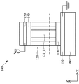
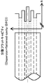
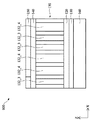
【解決手段】光学装置100は、第1の導電層110、第1の接合層120、光吸収層130、第2の接合層140、第2の導電層150、および基板160を含む。第1の接合層120は、第1の導電層120の上に配置される。光吸収層は複数のユニットセルを含み、各ユニットセルは複数のピラー構造を含み、サイズの異なるピラー構造を有することができる。
【選択図】図1
Description

110 第1の導電層
120 第1の接合層
130 光吸収層
131 ユニットセル
132_1、132_2、132_3、132_4、132_5、132_6 ピラー構造
140 第2の接合層
150 第2の導電層
160 基板
600 光学装置
610 フィルタ層
700 光学装置
900 光学装置
1000 光学装置
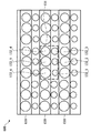
133_1、133_2、133_3、133_4、133_5、133_6、133_7、133_8、133_9、133_10、133_11、および133_12 ピラー構造
Claims (10)
- 第1の導電層、
前記第1の導電層の上に配置された第1の接合層、
前記第1の接合層の上に配置され、複数のユニットセルを含む光吸収層であって、前記ユニットセルの各々は複数のピラー構造を含み、前記ユニットセルの各々の前記複数のピラー構造は異なるサイズである光吸収層、
前記光吸収層の上に配置された第2の接合層、および
前記第2の接合層の上に配置された第2の導電層を含む光学装置。 - 前記ピラー構造の材料は、アモルファスシリコン(a−Si)およびアモルファスシリコン不純物であり、前記ユニットセルの各々のピラー構造の数は、少なくとも6つであり、前記ピラー構造の各々のサイズの幅は0.5um以下である請求項1に記載の光学装置。
- 前記ユニットセルの各々の前記ピラー構造の一部の上に配置された複数のフィルタ層をさらに含み、
前記ユニットセルの各々の前記ピラー構造の一部は、前記光吸収層により吸収される光の波長範囲において、所定の波長より小さいサイドバンドを有する請求項1に記載の光学装置。 - 前記フィルタ層の各々は、マルチフィルムを含む請求項3に記載の光学装置。
- 2つのユニットセル毎の前記ピラー構造の一部は、互いに隣接して配置され、前記ユニットセルの各々の屈折率は、W字状の変化を示す請求項3に記載の光学装置。
- 前記光吸収層により吸収される光の波長範囲は、450〜700nmであり、所定の波長は550nmである請求項3に記載の光学装置。
- 前記ユニットセルの各々の前記ピラー構造の一部の材料は、アモルファスシリコンおよびアモルファスシリコン不純物であり、前記ユニットセルの各々の前記ピラー構造の他の部分の材料は、ゲルマニウム(Ge)とゲルマニウムの不純物であり、前記ユニットセルの各々の前記ピラー構造の前記他の部分は、前記光吸収層により吸収される光の波長範囲の所定の波長以下のサイドバンドを有する請求項1に記載の光学装置。
- 前記ピラー構造の各々により吸収される光の波長は、前記ピラー構造のサイズの変化に伴って変化し、前記ピラー構造のサイズが大きいとき、前記ピラー構造により吸収される光の波長は大きく、前記ピラー構造のサイズが小さいとき、前記ピラー構造により吸収される光の波長は小さい請求項1に記載の光学装置。
- 前記第1の接合層の材料は、p型アモルファスシリコンであり、前記第2の接合層の材料は、n型アモルファスシリコンであり、前記第1の導電層および前記第2の導電層の材料はインジウムスズ酸化物(ITO)である請求項1に記載の光学装置。
- 前記第1の導電層の前記第1の接合層と反対の側に配置された基板をさらに含み、
前記基板の材料は、ガラスである請求項1に記載の光学装置。
Applications Claiming Priority (2)
| Application Number | Priority Date | Filing Date | Title |
|---|---|---|---|
| US16/849,094 US11355540B2 (en) | 2020-04-15 | 2020-04-15 | Optical device |
| US16/849,094 | 2020-04-15 |
Publications (2)
| Publication Number | Publication Date |
|---|---|
| JP2021170624A true JP2021170624A (ja) | 2021-10-28 |
| JP7300428B2 JP7300428B2 (ja) | 2023-06-29 |
Family
ID=71094112
Family Applications (1)
| Application Number | Title | Priority Date | Filing Date |
|---|---|---|---|
| JP2020136202A Active JP7300428B2 (ja) | 2020-04-15 | 2020-08-12 | 光学装置 |
Country Status (5)
| Country | Link |
|---|---|
| US (1) | US11355540B2 (ja) |
| EP (1) | EP3896748A1 (ja) |
| JP (1) | JP7300428B2 (ja) |
| CN (1) | CN113540272B (ja) |
| TW (1) | TWI777270B (ja) |
Citations (12)
| Publication number | Priority date | Publication date | Assignee | Title |
|---|---|---|---|---|
| US20100022499A1 (en) * | 2002-01-03 | 2010-01-28 | Yissum Research Development Company Of The Hebrew University Of Jerusalem | Heterocyclic compounds, combinatorial libraries thereof and methods of selecting drug leads |
| US20100127153A1 (en) * | 2007-05-07 | 2010-05-27 | Nxp B.V. | Photosensitive device and a method of manufacturing a photosensitive device |
| US20110041900A1 (en) * | 2009-08-18 | 2011-02-24 | Samsung Electronics Co., Ltd. | Solar cells having nanowires and methods of fabricating nanowires |
| WO2012161747A1 (en) * | 2011-05-20 | 2012-11-29 | Zena Technologies, Inc. | Passivated upstanding nanostructures and methods of making the same |
| JP2013239690A (ja) * | 2012-04-16 | 2013-11-28 | Sharp Corp | 超格子構造、前記超格子構造を備えた半導体装置および半導体発光装置、ならびに前記超格子構造の製造方法 |
| JP2014022499A (ja) * | 2012-07-17 | 2014-02-03 | Sharp Corp | 太陽電池 |
| JP2014049652A (ja) * | 2012-08-31 | 2014-03-17 | Panasonic Corp | 光起電力装置 |
| JP2015532725A (ja) * | 2012-08-13 | 2015-11-12 | プレジデント アンド フェローズ オブ ハーバード カレッジ | 光学装置、光フィルタの製造方法、画像形成装置およびその製造方法 |
| US20160204283A1 (en) * | 2013-08-18 | 2016-07-14 | Ramot At Tel-Aviv University Ltd. | Photovoltaic cell and method of fabricating the same |
| US20160240580A1 (en) * | 2015-02-12 | 2016-08-18 | Samsung Electronics Co., Ltd. | Photodetecting device and manufacturing method thereof, and image sensor and manufacturing method thereof |
| JP2017059739A (ja) * | 2015-09-18 | 2017-03-23 | ソニーセミコンダクタソリューションズ株式会社 | 固体撮像装置および電子機器 |
| JP2017120816A (ja) * | 2015-12-28 | 2017-07-06 | 凸版印刷株式会社 | 固体撮像素子およびその製造方法 |
Family Cites Families (14)
| Publication number | Priority date | Publication date | Assignee | Title |
|---|---|---|---|---|
| JP4235440B2 (ja) * | 2002-12-13 | 2009-03-11 | キヤノン株式会社 | 半導体デバイスアレイ及びその製造方法 |
| US20160111460A1 (en) | 2008-09-04 | 2016-04-21 | Zena Technologies, Inc. | Back-lit photodetector |
| US8282882B2 (en) * | 2010-08-23 | 2012-10-09 | Swapnajit Chakravarty | Photonic crystal slot waveguide miniature on-chip absorption spectrometer |
| JP2011138950A (ja) | 2009-12-28 | 2011-07-14 | Sony Corp | 半導体装置及び電子機器 |
| US9257583B2 (en) * | 2011-05-25 | 2016-02-09 | Hitachi, Ltd. | Solar cell |
| JP6070714B2 (ja) | 2012-10-18 | 2017-02-01 | 富士通株式会社 | 光電変換素子及びその製造方法 |
| KR102358584B1 (ko) | 2013-05-22 | 2022-02-04 | 시-위안 왕 | 마이크로구조-증강 흡수 감광성 디바이스 |
| FR3008546B1 (fr) | 2013-07-12 | 2015-08-07 | Commissariat Energie Atomique | Photodetecteur semi-transparent a jonction p-n structuree |
| GB2517186A (en) * | 2013-08-14 | 2015-02-18 | Norwegian University Of Science And Technology | Radial P-N junction nanowire solar cells |
| TW201727928A (zh) | 2016-01-28 | 2017-08-01 | 國立中興大學 | 紫外光感測器及其製造方法 |
| JP6759805B2 (ja) * | 2016-07-27 | 2020-09-23 | 富士通株式会社 | 光検出器、撮像装置及び光検出器の製造方法 |
| US10553733B2 (en) | 2016-11-29 | 2020-02-04 | Taiwan Semiconductor Manufacturing Co., Ltd. | QE approach by double-side, multi absorption structure |
| US10790323B2 (en) * | 2018-02-27 | 2020-09-29 | Advanced Semiconductor Engineering, Inc. | Semiconductor device packages and methods of manufacturing the same |
| US10651220B2 (en) | 2018-07-30 | 2020-05-12 | Taiwan Semiconductor Manufacturing Co., Ltd. | Narrow band filter with high transmission |
-
2020
- 2020-04-15 US US16/849,094 patent/US11355540B2/en active Active
- 2020-06-12 EP EP20179610.9A patent/EP3896748A1/en active Pending
- 2020-08-12 JP JP2020136202A patent/JP7300428B2/ja active Active
- 2020-10-13 TW TW109135295A patent/TWI777270B/zh active
- 2020-11-20 CN CN202011310012.6A patent/CN113540272B/zh active Active
Patent Citations (12)
| Publication number | Priority date | Publication date | Assignee | Title |
|---|---|---|---|---|
| US20100022499A1 (en) * | 2002-01-03 | 2010-01-28 | Yissum Research Development Company Of The Hebrew University Of Jerusalem | Heterocyclic compounds, combinatorial libraries thereof and methods of selecting drug leads |
| US20100127153A1 (en) * | 2007-05-07 | 2010-05-27 | Nxp B.V. | Photosensitive device and a method of manufacturing a photosensitive device |
| US20110041900A1 (en) * | 2009-08-18 | 2011-02-24 | Samsung Electronics Co., Ltd. | Solar cells having nanowires and methods of fabricating nanowires |
| WO2012161747A1 (en) * | 2011-05-20 | 2012-11-29 | Zena Technologies, Inc. | Passivated upstanding nanostructures and methods of making the same |
| JP2013239690A (ja) * | 2012-04-16 | 2013-11-28 | Sharp Corp | 超格子構造、前記超格子構造を備えた半導体装置および半導体発光装置、ならびに前記超格子構造の製造方法 |
| JP2014022499A (ja) * | 2012-07-17 | 2014-02-03 | Sharp Corp | 太陽電池 |
| JP2015532725A (ja) * | 2012-08-13 | 2015-11-12 | プレジデント アンド フェローズ オブ ハーバード カレッジ | 光学装置、光フィルタの製造方法、画像形成装置およびその製造方法 |
| JP2014049652A (ja) * | 2012-08-31 | 2014-03-17 | Panasonic Corp | 光起電力装置 |
| US20160204283A1 (en) * | 2013-08-18 | 2016-07-14 | Ramot At Tel-Aviv University Ltd. | Photovoltaic cell and method of fabricating the same |
| US20160240580A1 (en) * | 2015-02-12 | 2016-08-18 | Samsung Electronics Co., Ltd. | Photodetecting device and manufacturing method thereof, and image sensor and manufacturing method thereof |
| JP2017059739A (ja) * | 2015-09-18 | 2017-03-23 | ソニーセミコンダクタソリューションズ株式会社 | 固体撮像装置および電子機器 |
| JP2017120816A (ja) * | 2015-12-28 | 2017-07-06 | 凸版印刷株式会社 | 固体撮像素子およびその製造方法 |
Also Published As
| Publication number | Publication date |
|---|---|
| CN113540272B (zh) | 2024-05-03 |
| US20210327928A1 (en) | 2021-10-21 |
| TW202141770A (zh) | 2021-11-01 |
| JP7300428B2 (ja) | 2023-06-29 |
| TWI777270B (zh) | 2022-09-11 |
| US11355540B2 (en) | 2022-06-07 |
| CN113540272A (zh) | 2021-10-22 |
| EP3896748A1 (en) | 2021-10-20 |
Similar Documents
| Publication | Publication Date | Title |
|---|---|---|
| US8681291B2 (en) | Display apparatus | |
| US8368068B2 (en) | Display with photo sensor and manufacturing method thereof | |
| CN113434051B (zh) | 一种生理特征侦测识别方法和光侦测装置 | |
| US20230275105A1 (en) | Unit cell of display panel including integrated tft photodetector | |
| CN102792456A (zh) | 太阳能电池、太阳能电池板和具备太阳能电池的装置 | |
| TWI227562B (en) | Photoelectric conversion device, image scanning apparatus, and manufacturing method of the photoelectric conversion device | |
| TW201801340A (zh) | 半導體光檢測元件 | |
| TWI755525B (zh) | 光偵測薄膜、光偵測器件、光偵測顯示裝置及光偵測薄膜的製備方法 | |
| Xu et al. | Dual-gate photosensitive a-Si: H TFT array enabling fingerprint-sensor-integrated display application | |
| JP2010251496A (ja) | イメージセンサー | |
| JP7300428B2 (ja) | 光学装置 | |
| US7915648B2 (en) | Light-receiving element and display device | |
| JPH04291968A (ja) | フォトダイオード | |
| US11569406B2 (en) | Pin device and manufacturing method thereof, photosensitive device and display device | |
| JP2014003042A (ja) | 光センサ素子内蔵の液晶表示装置 | |
| JP5330877B2 (ja) | 光検出装置及び表示装置 | |
| JP4811397B2 (ja) | 受光素子および表示装置 | |
| WO2014072595A1 (fr) | Surface photovoltaïque polarisante | |
| JP5285365B2 (ja) | 受光素子および表示装置 | |
| KR20130109789A (ko) | 공간 광변조기 | |
| KR100759273B1 (ko) | 콜리메이터가 포함된 보호필름층을 이용하여 센싱 성능과신뢰성을 높이는 접촉형 광 감지센서 장치 | |
| JP2006330322A (ja) | 液晶表示装置 | |
| JP2015028959A (ja) | 太陽電池、太陽電池パネル、太陽電池を備えた装置、及び、太陽電池パネルを備えた装置 | |
| KR101612719B1 (ko) | 수광 소자 및 표시 장치 | |
| JP2011258849A (ja) | 放射線画像撮影装置 |
Legal Events
| Date | Code | Title | Description |
|---|---|---|---|
| A621 | Written request for application examination |
Free format text: JAPANESE INTERMEDIATE CODE: A621 Effective date: 20200812 |
|
| A131 | Notification of reasons for refusal |
Free format text: JAPANESE INTERMEDIATE CODE: A131 Effective date: 20210928 |
|
| A521 | Request for written amendment filed |
Free format text: JAPANESE INTERMEDIATE CODE: A523 Effective date: 20211223 |
|
| A02 | Decision of refusal |
Free format text: JAPANESE INTERMEDIATE CODE: A02 Effective date: 20220301 |
|
| A521 | Request for written amendment filed |
Free format text: JAPANESE INTERMEDIATE CODE: A523 Effective date: 20220426 |
|
| C60 | Trial request (containing other claim documents, opposition documents) |
Free format text: JAPANESE INTERMEDIATE CODE: C60 Effective date: 20220426 |
|
| A911 | Transfer to examiner for re-examination before appeal (zenchi) |
Free format text: JAPANESE INTERMEDIATE CODE: A911 Effective date: 20220509 |
|
| C21 | Notice of transfer of a case for reconsideration by examiners before appeal proceedings |
Free format text: JAPANESE INTERMEDIATE CODE: C21 Effective date: 20220517 |
|
| A912 | Re-examination (zenchi) completed and case transferred to appeal board |
Free format text: JAPANESE INTERMEDIATE CODE: A912 Effective date: 20220527 |
|
| C211 | Notice of termination of reconsideration by examiners before appeal proceedings |
Free format text: JAPANESE INTERMEDIATE CODE: C211 Effective date: 20220617 |
|
| C22 | Notice of designation (change) of administrative judge |
Free format text: JAPANESE INTERMEDIATE CODE: C22 Effective date: 20230124 |
|
| C23 | Notice of termination of proceedings |
Free format text: JAPANESE INTERMEDIATE CODE: C23 Effective date: 20230328 |
|
| A61 | First payment of annual fees (during grant procedure) |
Free format text: JAPANESE INTERMEDIATE CODE: A61 Effective date: 20230619 |
|
| R150 | Certificate of patent or registration of utility model |
Ref document number: 7300428 Country of ref document: JP Free format text: JAPANESE INTERMEDIATE CODE: R150 |