JP2021170637A - Manufacturing method of ultraviolet laser diode and ultraviolet laser diode - Google Patents
Manufacturing method of ultraviolet laser diode and ultraviolet laser diode Download PDFInfo
- Publication number
- JP2021170637A JP2021170637A JP2021065479A JP2021065479A JP2021170637A JP 2021170637 A JP2021170637 A JP 2021170637A JP 2021065479 A JP2021065479 A JP 2021065479A JP 2021065479 A JP2021065479 A JP 2021065479A JP 2021170637 A JP2021170637 A JP 2021170637A
- Authority
- JP
- Japan
- Prior art keywords
- laser diode
- ultraviolet laser
- region
- layer
- mesa structure
- Prior art date
- Legal status (The legal status is an assumption and is not a legal conclusion. Google has not performed a legal analysis and makes no representation as to the accuracy of the status listed.)
- Granted
Links
Images






Classifications
-
- H—ELECTRICITY
- H01—ELECTRIC ELEMENTS
- H01S—DEVICES USING THE PROCESS OF LIGHT AMPLIFICATION BY STIMULATED EMISSION OF RADIATION [LASER] TO AMPLIFY OR GENERATE LIGHT; DEVICES USING STIMULATED EMISSION OF ELECTROMAGNETIC RADIATION IN WAVE RANGES OTHER THAN OPTICAL
- H01S5/00—Semiconductor lasers
- H01S5/30—Structure or shape of the active region; Materials used for the active region
- H01S5/32—Structure or shape of the active region; Materials used for the active region comprising PN junctions, e.g. hetero- or double- heterostructures
- H01S5/323—Structure or shape of the active region; Materials used for the active region comprising PN junctions, e.g. hetero- or double- heterostructures in AIIIBV compounds, e.g. AlGaAs-laser, InP-based laser
- H01S5/32308—Structure or shape of the active region; Materials used for the active region comprising PN junctions, e.g. hetero- or double- heterostructures in AIIIBV compounds, e.g. AlGaAs-laser, InP-based laser emitting light at a wavelength less than 900 nm
-
- H—ELECTRICITY
- H01—ELECTRIC ELEMENTS
- H01S—DEVICES USING THE PROCESS OF LIGHT AMPLIFICATION BY STIMULATED EMISSION OF RADIATION [LASER] TO AMPLIFY OR GENERATE LIGHT; DEVICES USING STIMULATED EMISSION OF ELECTROMAGNETIC RADIATION IN WAVE RANGES OTHER THAN OPTICAL
- H01S5/00—Semiconductor lasers
- H01S5/30—Structure or shape of the active region; Materials used for the active region
- H01S5/34—Structure or shape of the active region; Materials used for the active region comprising quantum well or superlattice structures, e.g. single quantum well [SQW] lasers, multiple quantum well [MQW] lasers or graded index separate confinement heterostructure [GRINSCH] lasers
- H01S5/343—Structure or shape of the active region; Materials used for the active region comprising quantum well or superlattice structures, e.g. single quantum well [SQW] lasers, multiple quantum well [MQW] lasers or graded index separate confinement heterostructure [GRINSCH] lasers in AIIIBV compounds, e.g. AlGaAs-laser, InP-based laser
- H01S5/34333—Structure or shape of the active region; Materials used for the active region comprising quantum well or superlattice structures, e.g. single quantum well [SQW] lasers, multiple quantum well [MQW] lasers or graded index separate confinement heterostructure [GRINSCH] lasers in AIIIBV compounds, e.g. AlGaAs-laser, InP-based laser with a well layer based on Ga(In)N or Ga(In)P, e.g. blue laser
-
- H—ELECTRICITY
- H01—ELECTRIC ELEMENTS
- H01S—DEVICES USING THE PROCESS OF LIGHT AMPLIFICATION BY STIMULATED EMISSION OF RADIATION [LASER] TO AMPLIFY OR GENERATE LIGHT; DEVICES USING STIMULATED EMISSION OF ELECTROMAGNETIC RADIATION IN WAVE RANGES OTHER THAN OPTICAL
- H01S5/00—Semiconductor lasers
- H01S5/02—Structural details or components not essential to laser action
- H01S5/0206—Substrates, e.g. growth, shape, material, removal or bonding
-
- H—ELECTRICITY
- H01—ELECTRIC ELEMENTS
- H01S—DEVICES USING THE PROCESS OF LIGHT AMPLIFICATION BY STIMULATED EMISSION OF RADIATION [LASER] TO AMPLIFY OR GENERATE LIGHT; DEVICES USING STIMULATED EMISSION OF ELECTROMAGNETIC RADIATION IN WAVE RANGES OTHER THAN OPTICAL
- H01S5/00—Semiconductor lasers
- H01S5/04—Processes or apparatus for excitation, e.g. pumping, e.g. by electron beams
- H01S5/042—Electrical excitation ; Circuits therefor
- H01S5/0425—Electrodes, e.g. characterised by the structure
- H01S5/04256—Electrodes, e.g. characterised by the structure characterised by the configuration
- H01S5/04257—Electrodes, e.g. characterised by the structure characterised by the configuration having positive and negative electrodes on the same side of the substrate
-
- H—ELECTRICITY
- H01—ELECTRIC ELEMENTS
- H01S—DEVICES USING THE PROCESS OF LIGHT AMPLIFICATION BY STIMULATED EMISSION OF RADIATION [LASER] TO AMPLIFY OR GENERATE LIGHT; DEVICES USING STIMULATED EMISSION OF ELECTROMAGNETIC RADIATION IN WAVE RANGES OTHER THAN OPTICAL
- H01S5/00—Semiconductor lasers
- H01S5/20—Structure or shape of the semiconductor body to guide the optical wave ; Confining structures perpendicular to the optical axis, e.g. index or gain guiding, stripe geometry, broad area lasers, gain tailoring, transverse or lateral reflectors, special cladding structures, MQW barrier reflection layers
- H01S5/22—Structure or shape of the semiconductor body to guide the optical wave ; Confining structures perpendicular to the optical axis, e.g. index or gain guiding, stripe geometry, broad area lasers, gain tailoring, transverse or lateral reflectors, special cladding structures, MQW barrier reflection layers having a ridge or stripe structure
- H01S5/227—Buried mesa structure ; Striped active layer
- H01S5/2275—Buried mesa structure ; Striped active layer mesa created by etching
-
- H—ELECTRICITY
- H01—ELECTRIC ELEMENTS
- H01S—DEVICES USING THE PROCESS OF LIGHT AMPLIFICATION BY STIMULATED EMISSION OF RADIATION [LASER] TO AMPLIFY OR GENERATE LIGHT; DEVICES USING STIMULATED EMISSION OF ELECTROMAGNETIC RADIATION IN WAVE RANGES OTHER THAN OPTICAL
- H01S5/00—Semiconductor lasers
- H01S5/30—Structure or shape of the active region; Materials used for the active region
- H01S5/32—Structure or shape of the active region; Materials used for the active region comprising PN junctions, e.g. hetero- or double- heterostructures
- H01S5/3211—Structure or shape of the active region; Materials used for the active region comprising PN junctions, e.g. hetero- or double- heterostructures characterised by special cladding layers, e.g. details on band-discontinuities
- H01S5/3215—Structure or shape of the active region; Materials used for the active region comprising PN junctions, e.g. hetero- or double- heterostructures characterised by special cladding layers, e.g. details on band-discontinuities graded composition cladding layers
-
- H—ELECTRICITY
- H01—ELECTRIC ELEMENTS
- H01S—DEVICES USING THE PROCESS OF LIGHT AMPLIFICATION BY STIMULATED EMISSION OF RADIATION [LASER] TO AMPLIFY OR GENERATE LIGHT; DEVICES USING STIMULATED EMISSION OF ELECTROMAGNETIC RADIATION IN WAVE RANGES OTHER THAN OPTICAL
- H01S5/00—Semiconductor lasers
- H01S5/04—Processes or apparatus for excitation, e.g. pumping, e.g. by electron beams
- H01S5/042—Electrical excitation ; Circuits therefor
- H01S5/0425—Electrodes, e.g. characterised by the structure
- H01S5/04252—Electrodes, e.g. characterised by the structure characterised by the material
-
- H—ELECTRICITY
- H01—ELECTRIC ELEMENTS
- H01S—DEVICES USING THE PROCESS OF LIGHT AMPLIFICATION BY STIMULATED EMISSION OF RADIATION [LASER] TO AMPLIFY OR GENERATE LIGHT; DEVICES USING STIMULATED EMISSION OF ELECTROMAGNETIC RADIATION IN WAVE RANGES OTHER THAN OPTICAL
- H01S5/00—Semiconductor lasers
- H01S5/04—Processes or apparatus for excitation, e.g. pumping, e.g. by electron beams
- H01S5/042—Electrical excitation ; Circuits therefor
- H01S5/0425—Electrodes, e.g. characterised by the structure
- H01S5/04256—Electrodes, e.g. characterised by the structure characterised by the configuration
-
- H—ELECTRICITY
- H01—ELECTRIC ELEMENTS
- H01S—DEVICES USING THE PROCESS OF LIGHT AMPLIFICATION BY STIMULATED EMISSION OF RADIATION [LASER] TO AMPLIFY OR GENERATE LIGHT; DEVICES USING STIMULATED EMISSION OF ELECTROMAGNETIC RADIATION IN WAVE RANGES OTHER THAN OPTICAL
- H01S5/00—Semiconductor lasers
- H01S5/30—Structure or shape of the active region; Materials used for the active region
- H01S5/305—Structure or shape of the active region; Materials used for the active region characterised by the doping materials used in the laser structure
Landscapes
- Physics & Mathematics (AREA)
- Condensed Matter Physics & Semiconductors (AREA)
- General Physics & Mathematics (AREA)
- Electromagnetism (AREA)
- Optics & Photonics (AREA)
- Geometry (AREA)
- Semiconductor Lasers (AREA)
Abstract
【課題】発振閾値電流密度の低い紫外レーザダイオードの製造方法を提供する。【解決手段】基板上に、第1クラッド層と、発光層と、第2クラッド層と、をこの順に積層し、窒化物半導体積層体を形成する積層体形成工程(ステップS101)と、窒化物半導体積層体の少なくとも一部をエッチングして、メサ構造を形成し、平面視における共振器端面の長さとメサ構造の側面の長さとの比を、1:5以上1:500以下とするメサ構造形成工程(ステップS102)と、第1領域上の一部に、第1導電性材料を配置し、400℃以上の熱処理を施す第1電極形成工程(ステップS103)と、第2クラッド層上の領域であって、側面との距離が5μm以上となる領域に、第2導電性材料を配置する第2電極形成工程(ステップS104)と、を含む。【選択図】図1A method for manufacturing an ultraviolet laser diode having a low threshold current density for oscillation is provided. A laminate forming step (step S101) for forming a nitride semiconductor laminate by laminating a first clad layer, a light emitting layer, and a second clad layer on a substrate in this order; A mesa structure in which at least a part of a semiconductor laminate is etched to form a mesa structure, and a ratio of a length of a cavity facet to a length of a side surface of the mesa structure in plan view is 1:5 or more and 1:500 or less. A formation step (step S102); a first electrode formation step (step S103) of disposing a first conductive material on a part of the first region and performing heat treatment at 400 ° C. or higher; and a second electrode forming step (step S104) of arranging the second conductive material in the region, the region having a distance of 5 μm or more from the side surface. [Selection drawing] Fig. 1
Description
本開示は、紫外レーザダイオードの製造方法および紫外レーザダイオードに関する。 The present disclosure relates to a method for manufacturing an ultraviolet laser diode and an ultraviolet laser diode.
窒化物半導体は、直接遷移の再結合形態を有することから、高い再結合効率および高い光学利得を得ることができる点で、レーザダイオードのための材料として適している。例えば、特許文献1には、組成傾斜層を用いて、キャリアの注入効率を向上させる技術が開示されている。
Nitride semiconductors are suitable as materials for laser diodes because they have a direct transition recombination form, which allows them to obtain high recombination efficiency and high optical gain. For example,
上述のような従来技術は、紫外LED(Light Emission Diode)を前提とするものであり、紫外レーザダイオードについては、ほとんど検討されていないのが実情である。特に、紫外レーザダイオードにおける電極の配置に関しては、何ら知られていない。 The above-mentioned prior art is based on an ultraviolet LED (Light Emission Diode), and the fact is that ultraviolet laser diodes have hardly been studied. In particular, nothing is known about the arrangement of electrodes in the ultraviolet laser diode.
素子抵抗を低減させて、紫外レーザダイオードを低い閾値電流密度にて発振させるために、例えば、可視光のレーザダイオードの技術常識を参酌すると、図6Aおよび図6Bに示すように、第2電極6A,6Bを、メサ構造300A,300Bの第1電極5A,5B側の側面に極力近づけて配置する構成が適切であると考えられる。
In order to reduce the element resistance and oscillate the ultraviolet laser diode at a low threshold current density, for example, taking into account the common general knowledge of visible light laser diodes, as shown in FIGS. 6A and 6B, the
しかしながら、紫外レーザダイオードに、このような構成を適用しても、所望の低い発振閾値電流密度を得られないのが実情である。 However, even if such a configuration is applied to the ultraviolet laser diode, the desired low oscillation threshold current density cannot be obtained.
かかる事情に鑑みてなされた本開示の目的は、発振閾値電流密度の低い紫外レーザダイオードの製造方法および紫外レーザダイオードを提供することにある。 An object of the present disclosure made in view of such circumstances is to provide a method for manufacturing an ultraviolet laser diode having a low oscillation threshold current density and an ultraviolet laser diode.
一実施形態に係る紫外レーザダイオードの製造方法は、基板上に、第1導電型窒化物半導体層の第1領域および前記第1導電型窒化物半導体層の第2領域を有する第1クラッド層と、1つ以上の量子井戸層を有する発光層と、第2導電型窒化物半導体層を有する第2クラッド層と、をこの順に積層し、窒化物半導体積層体を形成する積層体形成工程と、前記窒化物半導体積層体の少なくとも一部をエッチングして、前記第2領域、前記発光層、および前記第2クラッド層を含むメサ構造を形成し、平面視における共振器端面の長さと前記メサ構造の側面の長さとの比を、1:5以上1:500以下とするメサ構造形成工程と、前記第1領域上の一部に、第1導電性材料を配置し、400℃以上の熱処理を施す第1電極形成工程と、前記第2クラッド層上の領域であって、前記側面との距離が5μm以上となる領域に、第2導電性材料を配置する第2電極形成工程と、を含むことを特徴とする。 The method for manufacturing an ultraviolet laser diode according to one embodiment includes a first clad layer having a first region of a first conductive nitride semiconductor layer and a second region of the first conductive nitride semiconductor layer on a substrate. A laminate forming step of laminating a light emitting layer having one or more quantum well layers and a second clad layer having a second conductive nitride semiconductor layer in this order to form a nitride semiconductor laminate. At least a part of the nitride semiconductor laminate is etched to form a mesa structure including the second region, the light emitting layer, and the second clad layer, and the length of the resonator end face and the mesa structure in a plan view are formed. A mesa structure forming step in which the ratio to the length of the side surface of the semiconductor is 1: 5 or more and 1: 500 or less, and a first conductive material is arranged in a part of the first region and heat-treated at 400 ° C. or higher. The first electrode forming step to be applied and the second electrode forming step of arranging the second conductive material in the region on the second clad layer where the distance from the side surface is 5 μm or more are included. It is characterized by that.
一実施形態に係る紫外レーザダイオードは、基板上に、第1導電型窒化物半導体層の第1領域および前記第1導電型窒化物半導体層の第2領域を有する第1クラッド層と、1つ以上の量子井戸層を有する発光層と、第2導電型窒化物半導体層を有する第2クラッド層と、をこの順に備え、前記第2領域、前記発光層、および前記第2クラッド層を含むメサ構造は、平面視における共振器端面の長さと前記メサ構造の側面の長さとの比が、1:5以上1:500以下であり、前記第2クラッド層上の領域であって、前記側面との距離が5μm以上となる領域に設けられる第2電極と、を備えることを特徴とする。 The ultraviolet laser diode according to the embodiment includes one clad layer having a first region of the first conductive nitride semiconductor layer and a second region of the first conductive nitride semiconductor layer on the substrate. A light emitting layer having the above quantum well layer and a second clad layer having a second conductive nitride semiconductor layer are provided in this order, and a mesa containing the second region, the light emitting layer, and the second clad layer. In the structure, the ratio of the length of the end face of the resonator and the length of the side surface of the mesa structure in a plan view is 1: 5 or more and 1: 500 or less, which is a region on the second clad layer and the side surface. It is characterized by including a second electrode provided in a region where the distance between the two is 5 μm or more.
また、一実施形態に係る紫外レーザダイオードは、基板上に、第1導電型窒化物半導体層の第1領域および前記第1導電型窒化物半導体層の第2領域を有する第1クラッド層と、1つ以上の量子井戸層を有する発光層と、第2導電型窒化物半導体層を有する第2クラッド層と、をこの順に備え、前記第2領域、前記発光層、および前記第2クラッド層を含むメサ構造は、平面視における共振器端面の長さと前記メサ構造の側面の長さとの比が、1:5以上1:500以下であり、前記第2クラッド層上の領域であって、前記共振器端面および前記側面との距離が5μm以上となる領域に設けられる第2電極と、を備えることを特徴とする。 Further, the ultraviolet laser diode according to the embodiment includes a first clad layer having a first region of the first conductive nitride semiconductor layer and a second region of the first conductive nitride semiconductor layer on the substrate. A light emitting layer having one or more quantum well layers and a second clad layer having a second conductive nitride semiconductor layer are provided in this order, and the second region, the light emitting layer, and the second clad layer are provided. The included mesa structure is a region on the second clad layer in which the ratio of the length of the end face of the resonator and the length of the side surface of the mesa structure in plan view is 1: 5 or more and 1: 500 or less. It is characterized by including a second electrode provided in a region where the distance between the end face of the resonator and the side surface is 5 μm or more.
なお、上記の発明の概要は、本発明の特徴の全てを列挙したものではない。また、これらの特徴群のサブコンビネーションもまた、発明となりうる。 The outline of the above invention does not list all the features of the present invention. Sub-combinations of these feature groups can also be inventions.
本開示によれば、発振閾値電流密度の低い紫外レーザダイオードの製造方法および紫外レーザダイオードを提供することが可能となる。 According to the present disclosure, it is possible to provide a method for manufacturing an ultraviolet laser diode having a low oscillation threshold current density and an ultraviolet laser diode.
以下、本発明の一実施形態について、図面を参照して詳細に説明する。なお、同一の構成要素には原則として同一の参照番号を付して、重複する説明を省略する。各図において、説明の便宜上、各構成の縦横の比率を実際の比率から誇張して示している。 Hereinafter, an embodiment of the present invention will be described in detail with reference to the drawings. In principle, the same components are given the same reference numbers, and duplicate explanations are omitted. In each figure, for convenience of explanation, the aspect ratio of each configuration is exaggerated from the actual ratio.
また、以下、説明の便宜上、「上」とは、図面に描かれた第2電極側を意味するものとし、「下」とは、図面に描かれた基板側を意味するものとする。ただし、「上」、「下」とは、便宜的に定められたものに過ぎず、限定的に解釈すべきものではない。 Further, hereinafter, for convenience of explanation, "upper" means the second electrode side drawn in the drawing, and "lower" means the substrate side drawn in the drawing. However, "above" and "below" are only defined for convenience and should not be interpreted in a limited manner.
また、「メサ構造」とは、ある面を基準としたときに、該面から連続し且つ高い位置に配置される構造を意味する。したがって、本明細書において、「メサ構造」とは、第1領域の上面を基準としたときに、該上面から連続し且つ高い位置に配置される、第2領域、発光層、および第2クラッド層を含む構造を意味するものとする。 Further, the "mesa structure" means a structure that is continuously arranged at a high position from a certain surface with respect to the surface. Therefore, in the present specification, the "mesa structure" refers to the second region, the light emitting layer, and the second clad, which are arranged continuously and at a high position from the upper surface of the first region as a reference. It shall mean a structure including layers.
また、本明細書において、「メサ構造の側面」とは、メサ構造における共振器端面以外の端面を意味するものとする。また、「メサ構造の一方の側面」とは、メサ構造における共振器端面以外の端面のうち、第1電極が形成されている側の側面を意味するものとし、「メサ構造の他方の側面」とは、メサ構造における共振器端面以外の端面のうち、第1電極が形成されていない側の側面を意味するものとする。 Further, in the present specification, the "side surface of the mesa structure" means an end face other than the resonator end face in the mesa structure. Further, "one side surface of the mesa structure" means the side surface of the mesa structure other than the resonator end surface on the side where the first electrode is formed, and "the other side surface of the mesa structure". Mesa means the side surface of the end face other than the resonator end face in the mesa structure on the side where the first electrode is not formed.
[第1実施形態]
<紫外レーザダイオードの製造方法>
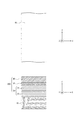
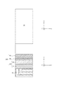
図1、および図2A乃至図2Eを参照して、第1実施形態に係る紫外レーザダイオード100の製造方法の一例について説明する。
[First Embodiment]
<Manufacturing method of ultraviolet laser diode>
An example of the method for manufacturing the
紫外レーザダイオード100の製造方法は、基板10上に、第1導電型窒化物半導体層の第1領域21および第1導電型窒化物半導体層の第2領域22を有する第1クラッド層20と、1つ以上の量子井戸層を有する発光層30と、第2導電型窒化物半導体層を有する第2クラッド層40と、をこの順に積層し、窒化物半導体積層体200を形成する積層体形成工程(ステップS101)と、窒化物半導体積層体200の少なくとも一部をエッチングして、第2領域22、発光層30、および第2クラッド層40を含むメサ構造300を形成し、平面視における共振器端面301の長さW1とメサ構造300の側面302の長さW2との比を、1:5以上1:500以下とするメサ構造形成工程(ステップS102)と、第1領域21上の一部に、第1導電性材料を配置し、400℃以上の熱処理を施す第1電極形成工程(ステップS103)と、第2クラッド層40上の領域であって、メサ構造300の側面302との距離が5μm以上となる領域に、第2導電性材料を配置する第2電極形成工程(ステップS104)と、を含む。
The method for manufacturing the
以下、各工程の詳細を順次説明する。 Hereinafter, details of each step will be described in sequence.
〔窒化物半導体積層体の形成工程:ステップS101〕
まず、図2Aに示すように、基板10上に、第1クラッド層20と、発光層30と、第2クラッド層40と、をこの順に積層し、窒化物半導体積層体200を形成する。第1クラッド層20は、第1導電型窒化物半導体層の第1領域21および第1導電型窒化物半導体層の第2領域22を有している。発光層30は、1つ以上の量子井戸層を有している。第2クラッド層40は、第2導電型窒化物半導体層を有している。
[Step of Forming Nitride Semiconductor Laminate: Step S101]
First, as shown in FIG. 2A, the first clad
窒化物半導体積層体200の厚みは、2μm程度以下であることが好ましく、1.5μm程度以下であることがより好ましい。
The thickness of the
第1クラッド層20、発光層30、および第2クラッド層40は、窒化物半導体で形成されることが好ましく、例えば、AlGaN、GaN、InGaN、BN、BAlN、BAlGaN、InAlGaNなどで形成されることが好ましい。
The first clad
第1クラッド層20は、第1導電型窒化物半導体で形成されることが好ましい。第2クラッド層40は、第2導電型窒化物半導体で形成されることが好ましい。第1導電型および第2導電型とは、一方がn型導電性を有するものであり、他方がp型導電性を有するものであることを意味する。例えば、第1導電型は、n型導電性を有する。例えば、第2導電型は、p型導電性を有する。
The first clad
発光層30は、その発光波長が特に限定されるものではないが、210nm以上360nm以下であることが好ましい。
The emission wavelength of the
窒化物半導体積層体200における各層の膜厚および構造は、当該分野で公知のものを採用することができる。なお、窒化物半導体積層体200は、基板10上に形成されたものであってもよい。
As the film thickness and structure of each layer in the
〔メサ構造の形成工程:ステップS102〕
次に、図2Bに示すように、窒化物半導体積層体200の少なくとも一部をエッチングして、第2領域22、発光層30、および第2クラッド層40を含むメサ構造300を形成する。
[Mesa structure forming step: step S102]
Next, as shown in FIG. 2B, at least a part of the
メサ構造300は、平面視における共振器端面301の長さW1が、平面視におけるメサ構造300の側面302の長さW2より短いことが好ましい。メサ構造300は、平面視における共振器端面301の長さW1とメサ構造300の側面302の長さW2との比が、1:5以上1:500以下であることが好ましい。例えば、図2Bにおいて、平面視における共振器端面301の長さW1とメサ構造300の側面302の長さW2との比は、1:8となっている。平面視における共振器端面301の長さW1とメサ構造300の側面302の長さW2との比を、当該範囲とすることで、共振方向において、広い領域で効率の良い電流注入が可能な紫外レーザダイオード100を実現できる。また、電流の狭窄効果により、発振閾値電流密度に到達させるための駆動電流を低減させることができるため、抵抗発熱を低減させ、素子寿命を向上させた紫外レーザダイオード100を実現できる。
In the
共振器端面301は、エッチング工程、あるいは、その他の工程により形成されてよい。メサ構造300の側面302は、エッチング工程により形成されることが好ましい。メサ構造300において、少なくとも側面302がエッチング工程により形成されることで、従来に係る紫外レーザダイオードと比較して、紫外レーザダイオード100の発振閾値電流密度を低くすることができる。
The
エッチング工程としては、特に限定されるものではないが、例えば、塩素系ガスによる反応性イオンエッチング、集束イオンビームエッチング、中性子粒子ビームエッチング、などのドライエッチング工程、ミリング工程が挙げられる。また、アルカリ溶液など、基板10及び窒化物半導体積層体200に対して侵食性のある溶液への浸漬によるウェットエッチング工程も挙げられる。さらには、前記ドライエッチング工程、ミリング工程と前記ウェットエッチングを組み合わせた工程も挙げられる。
The etching step is not particularly limited, and examples thereof include a dry etching step such as reactive ion etching with a chlorine-based gas, focused ion beam etching, and neutron particle beam etching, and a milling step. Further, a wet etching step by immersing the
〔第1電極の形成工程:ステップS103〕
次に、図2Cに示すように、第1領域21上の一部に、第1導電性材料を配置し、400℃以上の熱処理を施すことで、第1電極50を形成する。熱処理の温度を、少なくとも400℃以上とすることで、第1電極50の合金化が為され、コンタクト抵抗を低減させることができる。第1電極50は、図2Dに示す以外の位置にさらに複数追加して配置されても良い。例えば、平面視にてメサ構造300の左右にそれぞれ配置されても良い。
[Forming Step of First Electrode: Step S103]
Next, as shown in FIG. 2C, the
第1電極50の膜厚は、10nm以上400nm以下であることが好ましく、50nm以上であることがより好ましい。
The film thickness of the
第1領域21上の一部に、第1導電性材料を配置する方法は、特に限定されるものではない。例えば、フォトリソグラフィー法により、所定領域にのみ、第1導電性材料が配置されるように、パターニングおよびリフトオフを行ってもよい。例えば、第1領域21上に、第1導電性材料からなる導電膜を成膜した後に、所定領域にパターニングを行い、その後に、導電膜のエッチングあるいはミリングを行ってもよい。
The method of arranging the first conductive material in a part on the
熱処理工程としては、例えば、窒素雰囲気中のラピットサーマルプロセスなどが挙げられる。熱処理の温度は、400℃以上950℃以下であることが好ましく、800℃以上900℃以下であることがより好ましい。熱処理の時間は、30秒以上20分以下であることが好ましく、1分以上5分以下であることがより好ましい。熱処理の温度および熱処理の時間を当該範囲とすることで、第1電極50を適切に合金化することができる。なお、熱処理の温度とは、環境温度を意味する。
Examples of the heat treatment step include a rapid thermal process in a nitrogen atmosphere. The heat treatment temperature is preferably 400 ° C. or higher and 950 ° C. or lower, and more preferably 800 ° C. or higher and 900 ° C. or lower. The heat treatment time is preferably 30 seconds or more and 20 minutes or less, and more preferably 1 minute or more and 5 minutes or less. By setting the heat treatment temperature and the heat treatment time within the above ranges, the
〔第2電極の形成工程:ステップS104〕
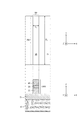
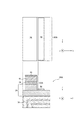
次に、図2Dおよび図2Eに示すように、第2クラッド層40上の領域であって、共振器端面301との距離DU,DDが5μm以上、およびメサ構造300の側面302との距離DR,DLが5μm以上となる領域に、第2導電性材料を配置し、第2電極60を形成する。
[Formation step of second electrode: step S104]
Next, as shown in FIG. 2D and FIG. 2E, a region on the
第2電極60の膜厚は、1nm以上200nm以下であることが好ましく、10nm以上100nm以下であることがより好ましい。
The film thickness of the
第2導電性材料は、図2Dに示すように、第2クラッド層40上の領域であって、共振器端面301との距離DU,DDが5μm以上、およびメサ構造300の側面302との距離DR,DLが5μm以上となる全ての領域に配置されてよい。例えば、第2導電性材料は、第2クラッド層40上の領域であって、共振器端面301との距離DU,DDが5μm、およびメサ構造300の側面302との距離DR,DLが5μmとなる全ての領域に配置されてよい。
The second conductive material, as shown in FIG. 2D, a region on the
また、第2導電性材料は、図2Eに示すように、第2クラッド層40上の領域であって、共振器端面301との距離DU,DDが5μm以上、およびメサ構造300の側面302との距離DR,DLが5μm以上となる一部の領域に配置されてよい。例えば、第2導電性材料は、第2クラッド層40上の領域であって、共振器端面301との距離DU,DDが5μm、メサ構造300の一方の側面302との距離DRが5μm、メサ構造300の他方の側面302との距離DLが15μmとなる領域に配置されてよい。
The second conductive material, as shown in FIG. 2E, a region on the
さらに、第2導電性材料は、第2クラッド層40上の領域であって、共振器端面301との距離DU,DDが5μm以上、およびメサ構造300の側面302との距離DR,DLが5μm以上となる領域において、ドット形状あるいはストライプ形状に配置されてよい。
Further, the second conductive material is a region on the
第2導電性材料が、メサ構造300の側面302との距離DR,DLが5μm以上となる領域に配置され、メサ構造300の側面302との距離DR,DLが5μm未満となる領域に配置されないことで、従来に係る紫外レーザダイオードと比較して、紫外レーザダイオード100の発振閾値電流密度を低くすることができる。
The second conductive material, the distance D R of the
特に、第2導電性材料が、メサ構造300の側面302との距離DR,DLが15μm以上となる領域に配置され、メサ構造300の側面302との距離DR,DLが15μm未満となる領域に配置されないことで、従来に係る紫外レーザダイオードと比較して、紫外レーザダイオード100の発振閾値電流密度の低下効果を安定化させることができる。
In particular, the second conductive material is arranged in a region where the distances D R and D L from the
第2クラッド層40上の領域に、第2導電性材料を配置する方法は、特に限定されるものではない。例えば、フォトリソグラフィー法により、所定領域にのみ、第2導電性材料が配置されるように、パターニングおよびリフトオフを行ってもよい。例えば、第2クラッド層40上に、第2導電性材料からなる導電膜を成膜した後に、所定領域にパターニングを行い、その後に、導電膜のエッチングを行ってもよい。なお、第2導電性材料が、第2クラッド層40上の領域に配置されるとは、必ずしも、第2導電性材料が、第2クラッド層40の上面と直接接して配置されることのみを意味するものではなく、第2導電性材料が、p−GaNからなるコンタクト層などを介して、第2クラッド層40上に配置されることも意味するものとする。
The method of arranging the second conductive material in the region on the second clad
ここで、図2Dおよび図2Eに示すような本実施形態に係る紫外レーザダイオード100と、図6Aおよび図6Bに示すような従来に係る紫外レーザダイオード100A,100Bと、を比較する。紫外レーザダイオード100は、第2電極60が、第2クラッド層40上の領域であって、メサ構造300の側面302との距離DR,DLが5μm以上となる領域に設けられている。一方、紫外レーザダイオード100Aは、第2電極6Aが、第2クラッド層4A上の全ての領域に設けられている。このような電極配置構造は、窒化物半導体積層体の全体に電力を満遍なく供給できる点で好ましいと考えられる。また、紫外レーザダイオード100Bは、第2電極6Bが、第2クラッド層4B上の領域であって、メサ構造の側面302Bとの距離が5μm未満となる領域に設けられている。このような電極配置構造は、第1電極5Bと第2電極6Bとを極力近づけられる点で好ましいと考えられる。
Here, the
詳細な測定結果([実施例]参照)は後述するが、図2Dおよび図2Eに示すような電極配置構造を有する紫外レーザダイオード100は、図6Aおよび図6Bに示すような電極配置構造を有する紫外レーザダイオード100A,100Bと比較して、発振閾値電流密度を低くすることができる。
Although detailed measurement results (see [Example]) will be described later, the
その理由は定かではないが、紫外レーザダイオードにおいて、メサ構造の側面との距離が5μm程度の領域における発光層は、結晶性が悪い。このため、紫外レーザダイオード100A,100Bでは、発光層3A,3Bの結晶性が悪い領域に流れた電流が、実質的に内部損失となり、発振閾値電流密度が増大してしまうと推察される。
Although the reason is not clear, in the ultraviolet laser diode, the light emitting layer in the region where the distance from the side surface of the mesa structure is about 5 μm has poor crystallinity. Therefore, in the
あるいは、紫外レーザダイオードにおいて、メサ構造の側面との距離が5μm程度の領域における発光層を含む複数の層は、メサ構造の側面にエッチングによるダメージが加わることで、結晶性が悪化する。このため、紫外レーザダイオード100A,100Bでは、結晶性が悪化した領域に供給された電力が、実質的に内部損失となり、発振閾値電流密度が増大してしまうと推察される。
Alternatively, in the ultraviolet laser diode, the plurality of layers including the light emitting layer in the region where the distance from the side surface of the mesa structure is about 5 μm deteriorates the crystallinity due to the damage caused by etching on the side surface of the mesa structure. Therefore, in the
なお、紫外レーザダイオード100は、紫外レーザダイオード100Aと比較して、平面視における第2電極の面積が小さく、紫外レーザダイオード100Bと比較して、平面視における第2電極の面積が大きい。したがって、紫外レーザダイオードの発振閾値電流密度は、第2電極の面積と、直接的に関係しないと推察される。
The
以上の任意工程を含む各工程を経ることにより、本実施形態に係る紫外レーザダイオード100を製造することができる。本実施形態に係る紫外レーザダイオード100は、第2電極60が、第2クラッド層40上の領域であって、メサ構造300の側面302との距離DR,DLが5μm以上となる領域に設けられている。これにより、従来に係る紫外レーザダイオード100A,100Bと比較して、発振閾値電流密度を低くすることができる。
The
<紫外レーザダイオード>
図3Aおよび図3Bを参照して、第1実施形態に係る紫外レーザダイオード100の構成の一例について説明する。
<Ultraviolet laser diode>
An example of the configuration of the
以下、各構成の詳細を順次説明する。なお、同一の構成要素に同一の参照番号を付しており、各構成要素の形状、膜厚などの説明は既述のとおりであり、重複する説明を省略する。 Hereinafter, details of each configuration will be described in sequence. The same component is given the same reference number, and the description of the shape, film thickness, etc. of each component is as described above, and duplicate description will be omitted.
〔基板〕
基板10は、特に限定されるものではなく、その上に、窒化物半導体積層体200(図2A参照)を積層することが可能であればよい。基板10としては、例えば、窒化アルミニウム単結晶基板、サファイア基板、サファイア基板上に窒化アルミニウムが成膜された複合基板などを用いることができる。基板10として、特に、窒化アルミニウム単結晶基板を用いることで、高品質な窒化物半導体積層体200を形成することができる。
〔substrate〕
The
〔第1クラッド層〕
第1クラッド層20は、基板10上に設けられている。第1クラッド層20は、第1導電型窒化物半導体層の第1領域21および第1導電型窒化物半導体層の第2領域22を有している。第1領域21および第2領域22は、同一の材料で形成されることが好ましい。第1領域21および第2領域22は、例えば、Al0.7Ga0.3Nで形成されることが好ましい。
[First clad layer]
The first clad
第1クラッド層20は、不純物によりドーピングされていてもよい。不純物としては、例えば、Si、Ge、C、Oなどが挙げられる。不純物としては、これらの不純物の何れか1つが選択されてもよいし、これらの不純物の複数が選択されてもよい。不純物の濃度は、特に限定されるものではないが、1×1017cm−3以上1×1020cm−3以下であることが好ましく、5×1018cm−3以上5×1019cm−3以下であることがより好ましい。
The first clad
〔発光層〕
発光層30は、第1クラッド層20上に設けられている。発光層30は、その発光波長が、210nm以上360nm以下であることが好ましい。
[Light emitting layer]
The
発光層30は、1つ以上の量子井戸層を有している。量子井戸層は、所望する発光波長により、その材料が、適宜選択されてよい。量子井戸層に用いられる材料としては、紫外領域の発光波長を得る目的である場合、例えば、AlxGa1−xN(0≦x≦0.8)などが挙げられる。
The
発光層30は、量子井戸層の上方若しくは下方、又は、その双方が、量子井戸層と異なる材料で形成された層により挟まれた構造を有している。このような層としては、例えば、10nm以上200nm以下のAlxGa1−xN(0.5≦x<0.7)層などが挙げられる。
The
発光層30は、一部が、不純物によりドーピングされていてもよい。不純物としては、例えば、Si、Cなどが挙げられる。なお、発光層30は、意図的に、不純物がドーピングされていない構造であってもよい。
The
〔第2クラッド層〕
第2クラッド層40は、発光層30上に設けられている。第2クラッド層40は、第2導電型窒化物半導体層を有している。第2クラッド層40は、全体または一部が、例えば、Mg、B、Be、Si、Liなどの第2導電型不純物を有さないことが好ましい。第2クラッド層40が第2導電型不純物を有さないことで、従来に係る紫外レーザダイオードと比較して、紫外レーザダイオード100の発振閾値電流密度を低くすることができる。
[Second clad layer]
The second clad
第2クラッド層40は、全体または一部が、組成傾斜層を含むことが好ましい。組成傾斜層とは、基板10の上面に対して垂直方向に、材料となる混晶の組成を連続的に変化させた層を意味する。第2クラッド層40が組成傾斜層を含むことで、紫外レーザダイオード100における電流の注入効率を向上させることができる。
The second clad
組成傾斜層は、例えば、AlGaN層で構成され、発光層30と第2クラッド層40との界面Xから遠ざかる方向に向かって、Al組成が1.0から連続的に減少していく層であってよい。第2クラッド層40が、このような組成傾斜層を含むことで、光閉じ込めおよび発光層30へのキャリア注入、および電子のブロック層としての役割を果たすことから、紫外レーザダイオード100の発振閾値電流密度を低くする効果が期待される。
The composition gradient layer is composed of, for example, an AlGaN layer, and is a layer in which the Al composition continuously decreases from 1.0 in the direction away from the interface X between the light emitting
上述した第2領域22、発光層30、および第2クラッド層40により、メサ構造300が形成される。メサ構造300は、側面の一部が、紫外レーザダイオード100の共振器端面301となっている。
The
〔第1電極〕
第1電極50は、第1領域21上に設けられている。第1電極50は、第1クラッド層20と電気的に接続される第1導電性材料で形成されることが好ましい。第1導電性材料としては、例えば、Mo、Nb、Zr、Ti、Al、W、Ni、Au、V、Inの何れかを含む合金などが挙げられる。第1導電性材料として、特に、V、Ti、Al、Ni、Auの何れかを含む合金を用いることで、コンタクト抵抗を低減させることができる。
[First electrode]
The
〔第2電極〕
第2電極60は、第2クラッド層40上に設けられている。第2電極60は、第2クラッド層40と電気的に接続される第2導電性材料で形成されることが好ましい。第2導電性材料としては、例えば、Ti、Pt、Ni、Pd、Au、Pt、Co、Cu、Ni、Ta、Ruの何れか又は何れかを含む合金などが挙げられる。第2導電性材料として、特に、Ti、Pt、Ni、Au、Pdの何れかを含む合金を用いることで、コンタクト抵抗を低減させることができる。
[Second electrode]
The
本実施形態に係る紫外レーザダイオード100は、第2電極60が、第2クラッド層40上の領域であって、メサ構造300の側面302との距離DR,DLが5μm以上となる領域に設けられている。これにより、従来に係る紫外レーザダイオード100A,100Bと比較して、発振閾値電流密度を低くすることができる。
[第2実施形態]
<紫外レーザダイオードの製造方法>
図4A乃至図4Eを参照して、第2実施形態に係る紫外レーザダイオード100Xの製造方法の一例について説明する。
[Second Embodiment]
<Manufacturing method of ultraviolet laser diode>
An example of a method for manufacturing the
第2実施形態に係る紫外レーザダイオード100Xの製造方法が、第1実施形態に係る紫外レーザダイオード100の製造方法と異なる点は、第1実施形態に係る紫外レーザダイオード100の製造方法が、共振器端面301およびメサ構造300の側面302をエッチング工程により形成するのに対して、第2実施形態に係る紫外レーザダイオード100Xの製造方法は、共振器端面301を劈開工程により形成し、メサ構造300Xの側面302をエッチング工程により形成する点である。その他の工程は、同様であるため、重複した説明を省略する。
The manufacturing method of the
〔窒化物半導体積層体の形成工程:ステップS101〕
まず、図4Aに示すように、基板10上に、第1クラッド層20と、発光層30と、第2クラッド層40と、をこの順に積層し、窒化物半導体積層体200を形成する。第1クラッド層20は、第1導電型窒化物半導体層の第1領域21および第1導電型窒化物半導体層の第2領域22を有している。発光層30は、1つ以上の量子井戸層を有している。第2クラッド層40は、第2導電型窒化物半導体層を有している。
[Step of Forming Nitride Semiconductor Laminate: Step S101]
First, as shown in FIG. 4A, the first clad
〔メサ構造の形成工程:ステップS102〕
次に、図4Bに示すように、窒化物半導体積層体200の少なくとも一部をエッチングあるいは劈開し、第2領域22、発光層30、および第2クラッド層40を含むメサ構造300Xを形成する。
[Mesa structure forming step: step S102]
Next, as shown in FIG. 4B, at least a part of the
メサ構造300Xは、平面視における共振器端面301の長さW1が、平面視におけるメサ構造300Xの側面302の長さW2より短いことが好ましい。メサ構造300Xは、平面視における共振器端面301の長さW1とメサ構造300Xの側面302の長さW2との比が、1:5以上1:500以下であることが好ましい。平面視における共振器端面301の長さW1とメサ構造300Xの側面302の長さW2との比を、当該範囲とすることで、共振方向において、広い領域で効率の良い電流注入が可能な紫外レーザダイオード100Xを実現できる。また、電流の狭窄効果により、発振閾値電流密度に到達させるための駆動電流を低減させることができるため、抵抗発熱を低減させ、素子寿命を向上させた紫外レーザダイオード100Xを実現できる。
In the
共振器端面301は、劈開工程により形成されることが好ましい。劈開工程とは、適切な各種工程により、ウエハの自然劈開面を露出させて切断する工程を意味する。劈開工程は、例えば、ウエハ表面又はウエハ裏面に、レーザ照射により変質層を形成する工程、あるいは、物理的接触により傷をつけて劈開面が形成される切掛を設けるスクライブ工程と、ウエハに応力を負荷して設けられた切掛を起点に劈開面を広げて露出させるブレーキング工程と、を含む。共振器端面301が劈開工程により形成されることで、紫外レーザダイオード100Xにおける発光効率を向上させることができる。
The
メサ構造300Xの側面302は、エッチング工程により形成されることが好ましい。メサ構造300Xにおいて、少なくとも側面302がエッチング工程により形成されることで、従来に係る紫外レーザダイオードと比較して、紫外レーザダイオード100Xの発振閾値電流密度を低くすることができる。
The
窒化物半導体積層体200に対して、エッチング工程あるいは劈開工程を施す順序は、エッチング工程が先で、劈開工程が後であることが好ましい。これにより、紫外レーザダイオード100Xにおける発光効率を向上させることができる。
It is preferable that the etching step or the cleavage step is performed on the
〔第1電極の形成工程:ステップS103〕
次に、図4Cに示すように、第1領域21上の一部に、第1導電性材料を配置し、400℃以上の熱処理を施すことで、第1電極50を形成する。熱処理の温度を、少なくとも400℃以上とすることで、第1電極50の合金化が為され、コンタクト抵抗を低減させることができる。
[Forming Step of First Electrode: Step S103]
Next, as shown in FIG. 4C, the
〔第2電極の形成工程:ステップS104〕
次に、図4Dおよび図4Eに示すように、第2クラッド層40上の領域であって、共振器端面301との距離が5μm以下、およびメサ構造300Xの側面302との距離DR,DLが5μm以上となる領域に、第2導電性材料を配置し、第2電極60Xを形成する。
[Formation step of second electrode: step S104]
Next, as shown in FIGS. 4D and 4E, a region on the
第2導電性材料は、図4Dに示すように、第2クラッド層40上の領域であって、共振器端面301との距離が5μm以下、およびメサ構造300Xの側面302との距離DR,DLが5μm以上となる全ての領域に配置されてよい。例えば、第2導電性材料は、第2クラッド層40上の領域であって、共振器端面301との距離が0μm、およびメサ構造300Xの側面302との第2電極60Xと距離DR,DLが5μmとなる全ての領域に配置されてよい。
The second conductive material, as shown in FIG. 4D, a region on the
また、第2導電性材料は、図4Eに示すように、第2クラッド層40上の領域であって、共振器端面301との距離が5μm以下、およびメサ構造300Xの側面302との距離DR,DLが5μm以上となる一部の領域に配置されてよい。例えば、第2導電性材料は、第2クラッド層40上の領域であって、共振器端面301との距離が0μm、メサ構造300Xの一方の側面302との距離DRが5μm、メサ構造300Xの他方の側面302との距離DLが15μmとなる領域に配置されてよい。
Further, as shown in FIG. 4E, the second conductive material is a region on the second clad
さらに、第2導電性材料は、第2クラッド層40上の領域であって、共振器端面301との距離が5μm以下、およびメサ構造300Xの側面302との距離DR,DLが5μm以上となる領域において、ドット形状あるいはストライプ形状に配置されてよい。
Further, the second conductive material is a region on the
第2導電性材料が、共振器端面301との距離が5μm以下となる領域に配置されることで、紫外レーザダイオード100Xにおける発振閾値電流密度を低くすることができる。
By arranging the second conductive material in a region where the distance from the
第2導電性材料が、メサ構造300Xの側面302との距離DR,DLが5μm以上となる領域に配置され、メサ構造300Xの側面302との距離DR,DLが5μm未満となる領域に配置されないことで、従来に係る紫外レーザダイオードと比較して、紫外レーザダイオード100Xの発振閾値電流密度を低くすることができる。
The second conductive material, the distance D R of the
特に、第2導電性材料が、メサ構造300Xの側面302との距離DR,DLが15μm以上となる領域に配置され、メサ構造300Xの側面302との距離DR,DLが15μm未満となる領域に配置されないことで、従来に係る紫外レーザダイオードと比較して、紫外レーザダイオード100Xの発振閾値電流密度の低下効果を安定化させることができる。
In particular, the second conductive material, the distance D R of the
以上の任意工程を含む各工程を経ることにより、本実施形態に係る紫外レーザダイオード100Xを製造することができる。本実施形態に係る紫外レーザダイオード100Xは、第2電極60Xが、第2クラッド層40上の領域であって、共振器端面301との距離が5μm以下、およびメサ構造300Xの側面302との距離DR,DLが5μm以上となる領域に設けられている。これにより、従来に係る紫外レーザダイオード100A,100Bと比較して、発振閾値電流密度を低くすることができる。
By going through each step including the above optional steps, the
[実施例]
<発振閾値電流密度の比較>
本実施形態に係る紫外レーザダイオードおよび従来に係る紫外レーザダイオードを用いて、それぞれの発振閾値電流密度を測定し、測定結果を比較した。
[Example]
<Comparison of oscillation threshold current density>
Using the ultraviolet laser diode according to the present embodiment and the ultraviolet laser diode according to the conventional method, the respective oscillation threshold current densities were measured, and the measurement results were compared.
〔実施例1〕
実施例1として、AlN基板上面に、1×1019cm−3のSiによりドーピングされたAl0.7Ga0.3Nからなる第1導電型窒化物半導体層(第1クラッド層)と、Al0.63Ga0.37Nからなる層により挟まれた9nmの発光層と、全体に渡って不純物を意図的にドーピングしていない、AlN基板上面に向かってAl組成を1.0から0.7まで連続的に減少させた第2導電型窒化物半導体層(第2クラッド層)と、、AlN基板上面に向かってAl組成を0.7から0.3まで連続的に減少させた層とGaN層からなるコンタクト層と、をこの順序で堆積させた窒化物半導体積層体について、エッチングにより第1クラッド層の一部を露出させ、共振器端面の法線方向に対して垂直な方向、すなわち<11−20>方向の長さW1が40μm、共振器端面の法線方向、すなわち<1−100>方向の長さW2が400μm以上である長方形のメサ構造を形成した。次に、露出した第1導電型窒化物半導体層の第1領域上に、Au、Al、Ni、Vを含む第1電極を形成した。第1電極は、800°C以上の熱処理が施された。さらに、メサ構造の一方の側面から、5μm以上10μm以下の領域全体(幅5μm)に亘ってAu、Niを含む第2導電性材料を配置し、450°C以上の熱処理を施して第2電極を形成した(図5参照)。さらに、劈開によりメサ構造を400μmの長さに分断し、2つの共振器端面を含む共振器、すなわち、平面視における共振器端面の長さとメサ構造の側面の長さとの比が1:10のメサ構造を有する共振器を含む紫外レーザダイオードを作製した。実施例1に係る紫外レーザダイオードの発振閾値電流密度を測定したところ、閾値電流密度16kA/cm2でレーザ発振が観測された(表1参照)。
[Example 1]
As the first embodiment, a first conductive nitride semiconductor layer (first clad layer) made of Al 0.7 Ga 0.3 N doped with 1 × 10 19 cm -3 Si is formed on the upper surface of the AlN substrate. A 9 nm light emitting layer sandwiched between layers made of Al 0.63 Ga 0.37 N and an Al composition of 1.0 to 0 toward the upper surface of the AlN substrate, which is not intentionally doped with impurities throughout. A second conductive nitride semiconductor layer (second clad layer) whose Al composition is continuously reduced to 0.7, and a layer whose Al composition is continuously reduced from 0.7 to 0.3 toward the upper surface of the AlN substrate. With respect to the nitride semiconductor laminate in which the contact layer composed of the GaN layer and the GaN layer are deposited in this order, a part of the first clad layer is exposed by etching, and the direction is perpendicular to the normal direction of the resonator end face. That is, a rectangular mesa structure having a length W 1 in the <11-20> direction of 40 μm and a length W 2 in the normal direction of the end face of the resonator, that is, the
〔実施例2〕
実施例2として、メサ構造の一方の側面から、10μm以上15μm以下の領域全体(幅5μm)に亘ってAu、Niを含む第2導電性材料を配置し、450°C以上の熱処理を施して第2電極を形成した。第2電極を形成する位置が異なる以外は、実施例1と同様の紫外レーザダイオードを作製した。実施例2に係る紫外レーザダイオードの発振閾値電流密度を測定したところ、閾値電流密度14kA/cm2でレーザ発振が観測された(表1参照)。
[Example 2]
As the second embodiment, a second conductive material containing Au and Ni is arranged over the entire region (width 5 μm) of 10 μm or more and 15 μm or less from one side surface of the mesa structure, and heat-treated at 450 ° C. or more. A second electrode was formed. An ultraviolet laser diode similar to that of Example 1 was produced except that the position where the second electrode was formed was different. When the oscillation threshold current density of the ultraviolet laser diode according to Example 2 was measured, laser oscillation was observed at a threshold current density of 14 kA / cm 2 (see Table 1).
〔実施例3〕
実施例3として、メサ構造の一方の側面から、15μm以上20μm以下の領域全体(幅5μm)に亘ってAu、Niを含む第2導電性材料を配置し、450°C以上の熱処理を施して第2電極を形成した。第2電極を形成する位置が異なる以外は、実施例1と同様の紫外レーザダイオードを作製した。実施例3に係る紫外レーザダイオードの発振閾値電流密度を測定したところ、閾値電流密度12kA/cm2でレーザ発振が観測された(表1参照)。
[Example 3]
As Example 3, a second conductive material containing Au and Ni is arranged from one side surface of the mesa structure over the entire region (width 5 μm) of 15 μm or more and 20 μm or less, and heat-treated at 450 ° C. or more. A second electrode was formed. An ultraviolet laser diode similar to that of Example 1 was produced except that the position where the second electrode was formed was different. When the oscillation threshold current density of the ultraviolet laser diode according to Example 3 was measured, laser oscillation was observed at a threshold current density of 12 kA / cm 2 (see Table 1).
〔比較例1〕
比較例1として、メサ構造の一方の側面から、3μm以上8μm以下の領域全体(幅5μm)に亘ってAu、Niを含む第2導電性材料を配置し、450°C以上の熱処理を施して第2電極を形成した。第2電極を形成する位置が異なる以外は、実施例1と同様の紫外レーザダイオードを作製した。比較例1に係る紫外レーザダイオードの発振閾値電流密度を測定したところ、閾値電流密度40kA/cm2でレーザ発振が観測された(表1参照)。
[Comparative Example 1]
As Comparative Example 1, a second conductive material containing Au and Ni was placed over the entire region (width 5 μm) of 3 μm or more and 8 μm or less from one side surface of the mesa structure, and heat-treated at 450 ° C. or more. A second electrode was formed. An ultraviolet laser diode similar to that of Example 1 was produced except that the position where the second electrode was formed was different. When the oscillation threshold current density of the ultraviolet laser diode according to Comparative Example 1 was measured, laser oscillation was observed at a threshold current density of 40 kA / cm 2 (see Table 1).
〔実施例4〕
実施例4として、第2クラッド層において、第2クラッド層の膜厚に対して基板上面に近い方から、0%以上15.5%未満の深さ領域において意図的に不純物を混入させず、第2クラッド層の膜厚に対して基板上面に近い方から、15.5%以上100%以下の範囲において1×1019cm−3の濃度のMgを意図的に混入した。それ以外は、実施例1と同様の紫外レーザダイオードを作製した。実施例4に係る紫外レーザダイオードの発振閾値電流密度を測定したところ、閾値電流密度17kA/cm2でレーザ発振が観測された(表1参照)。
[Example 4]
As the fourth embodiment, in the second clad layer, impurities are not intentionally mixed in the depth region of 0% or more and less than 15.5% from the side closer to the upper surface of the substrate with respect to the film thickness of the second clad layer. Mg having a concentration of 1 × 10 19 cm -3 was intentionally mixed in the range of 15.5% or more and 100% or less from the side closer to the upper surface of the substrate with respect to the film thickness of the second clad layer. Other than that, the same ultraviolet laser diode as in Example 1 was produced. When the oscillation threshold current density of the ultraviolet laser diode according to Example 4 was measured, laser oscillation was observed at a threshold current density of 17 kA / cm 2 (see Table 1).
〔実施例5〕
実施例5として、メサ構造の一方の側面から、10μm以上15μm以下の領域全体(幅5μm)に亘ってAu、Niを含む第2導電性材料を配置し、450°C以上の熱処理を施して第2電極を形成した。第2電極を形成する位置が異なる以外は、実施例4と同様の紫外レーザダイオードを作製した。実施例5に係る紫外レーザダイオードの発振閾値電流密度を測定したところ、閾値電流密度16kA/cm2でレーザ発振が観測された(表1参照)。
[Example 5]
As Example 5, a second conductive material containing Au and Ni is arranged from one side surface of the mesa structure over the entire region (width 5 μm) of 10 μm or more and 15 μm or less, and heat-treated at 450 ° C. or more. A second electrode was formed. An ultraviolet laser diode similar to that of Example 4 was produced except that the position where the second electrode was formed was different. When the oscillation threshold current density of the ultraviolet laser diode according to Example 5 was measured, laser oscillation was observed at a threshold current density of 16 kA / cm 2 (see Table 1).
〔実施例6〕
実施例6として、メサ構造の一方の側面から、15μm以上20μm以下の領域全体(幅5μm)に亘ってAu、Niを含む第2導電性材料を配置し、450°C以上の熱処理を施して第2電極を形成した。第2電極を形成する位置が異なる以外は、実施例4と同様の紫外レーザダイオードを作製した。実施例6に係る紫外レーザダイオードの発振閾値電流密度を測定したところ、閾値電流密度13kA/cm2でレーザ発振が観測された(表1参照)。
[Example 6]
As Example 6, a second conductive material containing Au and Ni is arranged from one side surface of the mesa structure over the entire region (width 5 μm) of 15 μm or more and 20 μm or less, and heat-treated at 450 ° C. or more. A second electrode was formed. An ultraviolet laser diode similar to that of Example 4 was produced except that the position where the second electrode was formed was different. When the oscillation threshold current density of the ultraviolet laser diode according to Example 6 was measured, laser oscillation was observed at a threshold current density of 13 kA / cm 2 (see Table 1).
〔比較例2〕
比較例2として、メサ構造の一方の側面から、3μm以上8μm以下の領域全体(幅5μm)に亘ってAu、Niを含む第2導電性材料を配置し、450°C以上の熱処理を施して第2電極を形成した。第2電極を形成する位置が異なる以外は、実施例4と同様の紫外レーザダイオードを作製した。比較例2に係る紫外レーザダイオードの発振閾値電流密度を測定したところ、閾値電流密度41kA/cm2でレーザ発振が観測された(表1参照)。
[Comparative Example 2]
As Comparative Example 2, a second conductive material containing Au and Ni was placed over the entire region (width 5 μm) of 3 μm or more and 8 μm or less from one side surface of the mesa structure, and heat-treated at 450 ° C. or more. A second electrode was formed. An ultraviolet laser diode similar to that of Example 4 was produced except that the position where the second electrode was formed was different. When the oscillation threshold current density of the ultraviolet laser diode according to Comparative Example 2 was measured, laser oscillation was observed at a threshold current density of 41 kA / cm 2 (see Table 1).
〔測定結果〕
以上の実施例1〜実施例6、比較例1、および比較例2に係る紫外レーザダイオードの発振閾値電流密度の測定結果を、表1にまとめた。
〔Measurement result〕
Table 1 summarizes the measurement results of the oscillation threshold current densities of the ultraviolet laser diodes according to the above Examples 1 to 6, Comparative Example 1, and Comparative Example 2.
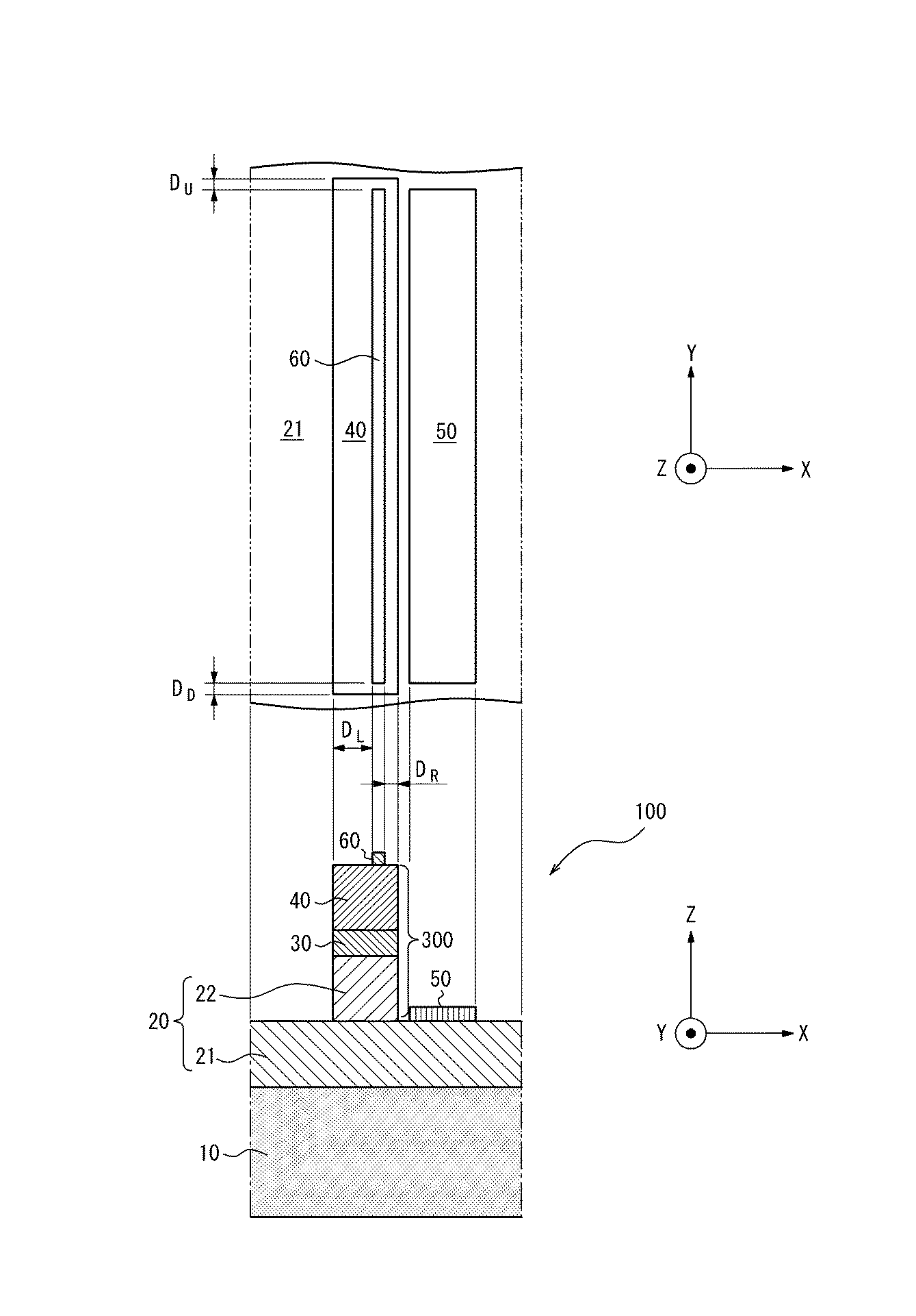
表1から、実施例1〜実施例6に係る紫外レーザダイオードは、比較例1および比較例2に係る紫外レーザダイオードと比較して、格段に低い発振閾値電流密度でレーザ発振することが理解される。 From Table 1, it is understood that the ultraviolet laser diodes according to Examples 1 to 6 oscillate at a significantly lower oscillation threshold current density than the ultraviolet laser diodes according to Comparative Examples 1 and 2. NS.
すなわち、第2クラッド層上の領域であって、エッチングにより形成されたメサ構造の側面との距離が5μm以上となる領域(例えば、5μm以上10μm以下の領域、10μm以上15μm以下の領域、15μm以上20μm以下の領域)に第2電極を備え、5μm未満となる領域に第2電極を備えない紫外レーザダイオードは、エッチングにより形成されたメサ構造の側面との距離が5μm未満となる領域(例えば、3μm以上8μm以下の領域)に第2電極を備える紫外レーザダイオードと比較して、格段に低い発振閾値電流密度でレーザ発振することが理解される。 That is, a region on the second clad layer in which the distance from the side surface of the mesa structure formed by etching is 5 μm or more (for example, a region of 5 μm or more and 10 μm or less, a region of 10 μm or more and 15 μm or less, a region of 15 μm or more). An ultraviolet laser diode having a second electrode in a region of 20 μm or less and not having a second electrode in a region of less than 5 μm has a region in which the distance from the side surface of the mesa structure formed by etching is less than 5 μm (for example,). It is understood that the laser oscillates at a significantly lower oscillation threshold current density as compared with the ultraviolet laser diode provided with the second electrode in the region (3 μm or more and 8 μm or less).
したがって、本実施形態に係る紫外レーザダイオードは、従来に係る紫外レーザダイオードと比較して、格段に低い発振閾値電流密度でレーザ発振可能であることが示唆される。 Therefore, it is suggested that the ultraviolet laser diode according to the present embodiment can oscillate a laser with a significantly lower oscillation threshold current density than the conventional ultraviolet laser diode.
また、表1から、実施例1〜実施例3に係る紫外レーザダイオードは、実施例4〜実施例6に係る紫外レーザダイオードと比較して、全体的に低い発振閾値電流密度でレーザ発振することが理解される。 Further, from Table 1, the ultraviolet laser diodes according to Examples 1 to 3 are laser-oscillated at an overall lower oscillation threshold current density than the ultraviolet laser diodes according to Examples 4 to 6. Is understood.
したがって、第2クラッド層の全体が第2導電型不純物を有さない紫外レーザダイオードは、第2クラッド層の一部に第2導電型不純物がドーピングされた紫外レーザダイオードと比較して、低い発振閾値電流密度でレーザ発振可能であることが示唆される。 Therefore, the ultraviolet laser diode in which the entire second clad layer does not have the second conductive type impurity has lower oscillation than the ultraviolet laser diode in which a part of the second clad layer is doped with the second conductive type impurity. It is suggested that laser oscillation is possible at the threshold current density.
<変形例>
本実施形態において、窒化物半導体積層体を積層する際における「この順」とは、少なくともこの順で各層(例えば、第1クラッド層、発光層、第2クラッド層)が積層されたものであれば特に制限されず、各層の間あるいは各層の上下に、さらに別の層を有していてもよい。
<Modification example>
In the present embodiment, the "in this order" when laminating the nitride semiconductor laminates means that the layers (for example, the first clad layer, the light emitting layer, and the second clad layer) are laminated in at least this order. The present invention is not particularly limited, and another layer may be provided between the layers or above and below each layer.
本実施形態に係る紫外レーザダイオードの製造方法は、メサ構造形成工程の後に、第2クラッド層40上の領域であって、少なくとも、メサ構造300の側面との距離が5μm未満となる領域に、絶縁層を形成する絶縁層形成工程をさらに含んでいてもよい。これにより、紫外レーザダイオード100,100Xの電流駆動時において、第1導電性材料と第2導電性材料との間の漏れ電流を抑制することができる。
In the method for manufacturing an ultraviolet laser diode according to the present embodiment, after the mesa structure forming step, a region on the second clad
<その他の変形例>
本発明は上記の実施形態および変形例に限定されるものではない。例えば、上述の各種の処理は、記載にしたがって時系列に実行されるのみならず、処理を実行する装置の処理能力あるいは必要に応じて並列的にあるいは個別に実行されてもよい。その他、本発明の趣旨を逸脱しない範囲で適宜変更が可能である。
<Other variants>
The present invention is not limited to the above embodiments and modifications. For example, the various processes described above may not only be executed in chronological order according to the description, but may also be executed in parallel or individually as required by the processing capacity of the device that executes the processes. In addition, changes can be made as appropriate without departing from the spirit of the present invention.
上述の実施形態は代表的な例として説明したが、本開示の趣旨及び範囲内で、多くの変更及び置換ができることは当業者に明らかである。したがって、本発明は、上述の実施形態により制限するものと解するべきではなく、特許請求の範囲から逸脱することなく、種々の変形や変更が可能である。例えば、実施形態のフローチャートに記載の複数の工程を1つに組み合わせたり、あるいは1つの工程を分割したりすることが可能である。 Although the above embodiments have been described as representative examples, it will be apparent to those skilled in the art that many modifications and substitutions can be made within the spirit and scope of the present disclosure. Therefore, the present invention should not be construed as being limited by the above-described embodiments, and various modifications and modifications can be made without departing from the scope of claims. For example, it is possible to combine a plurality of steps described in the flowchart of the embodiment into one, or to divide one step.
10 基板
20 第1クラッド層
21 第1領域
22 第2領域
30 発光層
40 第2クラッド層
50 第1電極
60 第2電極
60X 第2電極
100 紫外レーザダイオード
100X 紫外レーザダイオード
100A 紫外レーザダイオード
100B 紫外レーザダイオード
200 窒化物半導体積層体
300 メサ構造
300X メサ構造
300A メサ構造
300B メサ構造
301 共振器端面
302 メサ構造の側面
10
Claims (17)
前記窒化物半導体積層体の少なくとも一部をエッチングして、前記第2領域、前記発光層、および前記第2クラッド層を含むメサ構造を形成し、平面視における共振器端面の長さと前記メサ構造の側面の長さとの比を、1:5以上1:500以下とするメサ構造形成工程と、
前記第1領域上の一部に、第1導電性材料を配置し、400℃以上の熱処理を施す第1電極形成工程と、
前記第2クラッド層上の領域であって、前記側面との距離が5μm以上となる領域に、第2導電性材料を配置する第2電極形成工程と、
を含む、紫外レーザダイオードの製造方法。 On the substrate, a first clad layer having a first region of the first conductive nitride semiconductor layer and a second region of the first conductive nitride semiconductor layer, and a light emitting layer having one or more quantum well layers. , A laminate forming step of laminating a second clad layer having a second conductive nitride semiconductor layer in this order to form a nitride semiconductor laminate.
At least a part of the nitride semiconductor laminate is etched to form a mesa structure including the second region, the light emitting layer, and the second clad layer, and the length of the resonator end face and the mesa structure in a plan view are formed. The mesa structure forming step in which the ratio to the length of the side surface of the mesa structure is 1: 5 or more and 1: 500 or less.
A first electrode forming step in which a first conductive material is arranged in a part on the first region and heat treatment is performed at 400 ° C. or higher, and
A second electrode forming step of arranging the second conductive material in a region on the second clad layer where the distance from the side surface is 5 μm or more.
A method for manufacturing an ultraviolet laser diode, including.
前記側面を、エッチング工程により形成する、
請求項1に記載の紫外レーザダイオードの製造方法。 The mesa structure forming step is
The side surface is formed by an etching process.
The method for manufacturing an ultraviolet laser diode according to claim 1.
前記共振器端面を、劈開工程により形成する、
請求項1又は2に記載の紫外レーザダイオードの製造方法。 The mesa structure forming step is
The resonator end face is formed by a cleavage step.
The method for manufacturing an ultraviolet laser diode according to claim 1 or 2.
前記共振器端面との距離が5μm以下となる領域に、前記第2導電性材料を配置する、
請求項3に記載の紫外レーザダイオードの製造方法。 The second electrode forming step is
The second conductive material is arranged in a region where the distance from the resonator end face is 5 μm or less.
The method for manufacturing an ultraviolet laser diode according to claim 3.
前記第2クラッド層上の領域であって、少なくとも、前記側面との距離が5μm未満となる領域に、絶縁層を形成する絶縁層形成工程をさらに含む、
請求項1から4のいずれか一項に記載の紫外レーザダイオードの製造方法。 After the mesa structure forming step,
An insulating layer forming step of forming an insulating layer is further included in the region on the second clad layer, at least in a region where the distance from the side surface is less than 5 μm.
The method for manufacturing an ultraviolet laser diode according to any one of claims 1 to 4.
請求項1から5のいずれか一項に記載の紫外レーザダイオードの製造方法。 The substrate is an aluminum nitride single crystal substrate.
The method for manufacturing an ultraviolet laser diode according to any one of claims 1 to 5.
請求項1から6のいずれか一項に記載の紫外レーザダイオードの製造方法。 The light emitting layer has an emission wavelength of 210 nm or more and 360 nm or less.
The method for manufacturing an ultraviolet laser diode according to any one of claims 1 to 6.
前記第2領域、前記発光層、および前記第2クラッド層を含むメサ構造は、平面視における共振器端面の長さと前記メサ構造の側面の長さとの比が、1:5以上1:500以下であり、
前記第2クラッド層上の領域であって、前記側面との距離が5μm以上となる領域に設けられる第2電極と、
を備える紫外レーザダイオード。 On the substrate, a first clad layer having a first region of the first conductive nitride semiconductor layer and a second region of the first conductive nitride semiconductor layer, and a light emitting layer having one or more quantum well layers. , A second clad layer having a second conductive nitride semiconductor layer, and the like are provided in this order.
In the mesa structure including the second region, the light emitting layer, and the second clad layer, the ratio of the length of the resonator end face to the length of the side surface of the mesa structure in a plan view is 1: 5 or more and 1: 500 or less. And
A second electrode provided in a region on the second clad layer where the distance from the side surface is 5 μm or more.
Ultraviolet laser diode with.
請求項8に記載の紫外レーザダイオード。 The second clad layer has no second conductive impurities in whole or in part.
The ultraviolet laser diode according to claim 8.
請求項8又は9に記載の紫外レーザダイオード。 The second clad layer includes a composition gradient layer in whole or in part.
The ultraviolet laser diode according to claim 8 or 9.
請求項8から10のいずれか一項に記載の紫外レーザダイオード。 The substrate is an aluminum nitride single crystal substrate.
The ultraviolet laser diode according to any one of claims 8 to 10.
請求項8から11のいずれか一項に記載の紫外レーザダイオード。 The light emitting layer has an emission wavelength of 210 nm or more and 360 nm or less.
The ultraviolet laser diode according to any one of claims 8 to 11.
前記第2領域、前記発光層、および前記第2クラッド層を含むメサ構造は、平面視における共振器端面の長さと前記メサ構造の側面の長さとの比が、1:5以上1:500以下であり、
前記第2クラッド層上の領域であって、前記共振器端面および前記側面との距離が5μm以上となる領域に設けられる第2電極と、
を備える紫外レーザダイオード。 On the substrate, a first clad layer having a first region of the first conductive nitride semiconductor layer and a second region of the first conductive nitride semiconductor layer, and a light emitting layer having one or more quantum well layers. , A second clad layer having a second conductive nitride semiconductor layer, and the like are provided in this order.
In the mesa structure including the second region, the light emitting layer, and the second clad layer, the ratio of the length of the resonator end face to the length of the side surface of the mesa structure in a plan view is 1: 5 or more and 1: 500 or less. And
A second electrode provided in a region on the second clad layer where the distance between the resonator end face and the side surface is 5 μm or more.
Ultraviolet laser diode with.
請求項13に記載の紫外レーザダイオード。 The second clad layer has no second conductive impurities in whole or in part.
The ultraviolet laser diode according to claim 13.
請求項13又は14に記載の紫外レーザダイオード The second clad layer includes a composition gradient layer in whole or in part.
The ultraviolet laser diode according to claim 13 or 14.
請求項13から15のいずれか一項に記載の紫外レーザダイオード。 The substrate is an aluminum nitride single crystal substrate.
The ultraviolet laser diode according to any one of claims 13 to 15.
請求項13から16のいずれか一項に記載の紫外レーザダイオード。 The light emitting layer has an emission wavelength of 210 nm or more and 360 nm or less.
The ultraviolet laser diode according to any one of claims 13 to 16.
Applications Claiming Priority (2)
| Application Number | Priority Date | Filing Date | Title |
|---|---|---|---|
| JP2020072539 | 2020-04-14 | ||
| JP2020072539 | 2020-04-14 |
Publications (2)
| Publication Number | Publication Date |
|---|---|
| JP2021170637A true JP2021170637A (en) | 2021-10-28 |
| JP7563696B2 JP7563696B2 (en) | 2024-10-08 |
Family
ID=78006493
Family Applications (1)
| Application Number | Title | Priority Date | Filing Date |
|---|---|---|---|
| JP2021065479A Active JP7563696B2 (en) | 2020-04-14 | 2021-04-07 | Method for manufacturing ultraviolet laser diode and ultraviolet laser diode |
Country Status (2)
| Country | Link |
|---|---|
| US (2) | US12126141B2 (en) |
| JP (1) | JP7563696B2 (en) |
Citations (11)
| Publication number | Priority date | Publication date | Assignee | Title |
|---|---|---|---|---|
| JP2000196144A (en) * | 1998-12-28 | 2000-07-14 | Sanyo Electric Co Ltd | Semiconductor light emitting element |
| JP2000299532A (en) * | 1999-02-10 | 2000-10-24 | Nichia Chem Ind Ltd | Nitride semiconductor laser element |
| JP2000349398A (en) * | 1999-06-04 | 2000-12-15 | Nichia Chem Ind Ltd | Nitride semiconductor light emitting device and method of manufacturing the same |
| JP2001203389A (en) * | 1994-01-28 | 2001-07-27 | Nichia Chem Ind Ltd | Gallium nitride based compound semiconductor light emitting device and method for forming electrodes thereof |
| KR20010074543A (en) * | 2000-01-24 | 2001-08-04 | 이데이 노부유끼 | Semiconductor light emitting device |
| JP2002043692A (en) * | 2000-05-17 | 2002-02-08 | Sony Corp | Semiconductor laser and method of manufacturing the same |
| US20020175324A1 (en) * | 1998-01-14 | 2002-11-28 | Manijeh Razeghi | III-Nitride optoelectronic device |
| US20070195851A1 (en) * | 2006-02-21 | 2007-08-23 | Samsung Electronics Co., Ltd. | Semiconductor laser diode having ridge |
| US20090092165A1 (en) * | 2007-10-09 | 2009-04-09 | Seoul Opto Device Co., Ltd. | Laser diode having nano patterns and method of fabricating the same |
| JP2009123969A (en) * | 2007-11-15 | 2009-06-04 | Tohoku Univ | Ultraviolet nitride semiconductor light emitting device and manufacturing method thereof |
| JP2018532265A (en) * | 2015-09-17 | 2018-11-01 | クリスタル アイエス, インコーポレーテッドCrystal Is, Inc. | Ultraviolet light emitting device incorporating two-dimensional hole gas |
Family Cites Families (2)
| Publication number | Priority date | Publication date | Assignee | Title |
|---|---|---|---|---|
| JP4805887B2 (en) * | 2007-09-05 | 2011-11-02 | 株式会社東芝 | Semiconductor laser device |
| US11757250B2 (en) * | 2019-12-23 | 2023-09-12 | Kyocera Sld Laser, Inc. | Specialized mobile light device configured with a gallium and nitrogen containing laser source |
-
2021
- 2021-04-07 JP JP2021065479A patent/JP7563696B2/en active Active
- 2021-04-14 US US17/229,875 patent/US12126141B2/en active Active
-
2024
- 2024-09-18 US US18/888,156 patent/US20250015562A1/en active Pending
Patent Citations (13)
| Publication number | Priority date | Publication date | Assignee | Title |
|---|---|---|---|---|
| JP2001203389A (en) * | 1994-01-28 | 2001-07-27 | Nichia Chem Ind Ltd | Gallium nitride based compound semiconductor light emitting device and method for forming electrodes thereof |
| US20020175324A1 (en) * | 1998-01-14 | 2002-11-28 | Manijeh Razeghi | III-Nitride optoelectronic device |
| JP2000196144A (en) * | 1998-12-28 | 2000-07-14 | Sanyo Electric Co Ltd | Semiconductor light emitting element |
| JP2000299532A (en) * | 1999-02-10 | 2000-10-24 | Nichia Chem Ind Ltd | Nitride semiconductor laser element |
| JP2000349398A (en) * | 1999-06-04 | 2000-12-15 | Nichia Chem Ind Ltd | Nitride semiconductor light emitting device and method of manufacturing the same |
| KR20010074543A (en) * | 2000-01-24 | 2001-08-04 | 이데이 노부유끼 | Semiconductor light emitting device |
| JP2002043692A (en) * | 2000-05-17 | 2002-02-08 | Sony Corp | Semiconductor laser and method of manufacturing the same |
| US20070195851A1 (en) * | 2006-02-21 | 2007-08-23 | Samsung Electronics Co., Ltd. | Semiconductor laser diode having ridge |
| JP2007227912A (en) * | 2006-02-21 | 2007-09-06 | Samsung Electronics Co Ltd | Semiconductor laser diode having ridge structure |
| US20090092165A1 (en) * | 2007-10-09 | 2009-04-09 | Seoul Opto Device Co., Ltd. | Laser diode having nano patterns and method of fabricating the same |
| JP2009094471A (en) * | 2007-10-09 | 2009-04-30 | Seoul Opto Devices Co Ltd | Laser diode having nanopattern and method for manufacturing the same |
| JP2009123969A (en) * | 2007-11-15 | 2009-06-04 | Tohoku Univ | Ultraviolet nitride semiconductor light emitting device and manufacturing method thereof |
| JP2018532265A (en) * | 2015-09-17 | 2018-11-01 | クリスタル アイエス, インコーポレーテッドCrystal Is, Inc. | Ultraviolet light emitting device incorporating two-dimensional hole gas |
Also Published As
| Publication number | Publication date |
|---|---|
| JP7563696B2 (en) | 2024-10-08 |
| US20250015562A1 (en) | 2025-01-09 |
| US20210320477A1 (en) | 2021-10-14 |
| US12126141B2 (en) | 2024-10-22 |
Similar Documents
| Publication | Publication Date | Title |
|---|---|---|
| JP4924185B2 (en) | Nitride semiconductor light emitting device | |
| JP6152848B2 (en) | Semiconductor light emitting device | |
| US20120213242A1 (en) | Semiconductor laser device | |
| JP2013065630A (en) | Semiconductor light-emitting element, wafer, method of manufacturing semiconductor light-emitting element, and method of manufacturing wafer | |
| JP2011124442A (en) | Semiconductor laser device, and method of manufacturing the same | |
| JP2021190687A (en) | Nitride semiconductor element | |
| JP3375042B2 (en) | Nitride semiconductor laser device | |
| JPWO2017017928A1 (en) | Nitride semiconductor laser device | |
| JPH07176826A (en) | Gallium nitride compound semiconductor laser device | |
| US20080298411A1 (en) | Nitride-based semiconductor laser device and method of manufacturing the same | |
| JP2006203171A (en) | Nitride semiconductor device and manufacturing method thereof | |
| CN101950922A (en) | Laser diode element, its driving method and laser diode device | |
| JP2001144378A (en) | Compound semiconductor light emitting device and method of manufacturing the same | |
| JP2022138095A (en) | Nitride semiconductor laser diode and manufacturing method thereof | |
| JP2009170895A (en) | Nitride semiconductor device and semiconductor laser | |
| US20210313760A1 (en) | Method for manufacturing semiconductor laser diode and semiconductor laser diode | |
| JP3502527B2 (en) | Nitride semiconductor laser device | |
| JP7563696B2 (en) | Method for manufacturing ultraviolet laser diode and ultraviolet laser diode | |
| JP4493041B2 (en) | Nitride semiconductor light emitting device | |
| JP7560058B2 (en) | Manufacturing method of semiconductor laser diode, semiconductor laser diode | |
| JP2011044648A (en) | Nitride semiconductor laser device and method of manufacturing the same | |
| JP2002261370A (en) | Method for manufacturing nitride semiconductor device | |
| JP2007235181A (en) | Semiconductor light emitting device manufacturing method and semiconductor light emitting device manufacturing method | |
| JP2004311678A (en) | Semiconductor element with laminated metal film | |
| JP6821921B2 (en) | Laser element |
Legal Events
| Date | Code | Title | Description |
|---|---|---|---|
| A621 | Written request for application examination |
Free format text: JAPANESE INTERMEDIATE CODE: A621 Effective date: 20240216 |
|
| A977 | Report on retrieval |
Free format text: JAPANESE INTERMEDIATE CODE: A971007 Effective date: 20240827 |
|
| TRDD | Decision of grant or rejection written | ||
| A01 | Written decision to grant a patent or to grant a registration (utility model) |
Free format text: JAPANESE INTERMEDIATE CODE: A01 Effective date: 20240903 |
|
| A61 | First payment of annual fees (during grant procedure) |
Free format text: JAPANESE INTERMEDIATE CODE: A61 Effective date: 20240917 |
|
| R150 | Certificate of patent or registration of utility model |
Ref document number: 7563696 Country of ref document: JP Free format text: JAPANESE INTERMEDIATE CODE: R150 |