JP2022014007A - Semiconductor storage device - Google Patents
Semiconductor storage device Download PDFInfo
- Publication number
- JP2022014007A JP2022014007A JP2020116116A JP2020116116A JP2022014007A JP 2022014007 A JP2022014007 A JP 2022014007A JP 2020116116 A JP2020116116 A JP 2020116116A JP 2020116116 A JP2020116116 A JP 2020116116A JP 2022014007 A JP2022014007 A JP 2022014007A
- Authority
- JP
- Japan
- Prior art keywords
- storage device
- semiconductor storage
- conductive layer
- semiconductor
- block
- Prior art date
- Legal status (The legal status is an assumption and is not a legal conclusion. Google has not performed a legal analysis and makes no representation as to the accuracy of the status listed.)
- Pending
Links
Images











Classifications
-
- H—ELECTRICITY
- H10—SEMICONDUCTOR DEVICES; ELECTRIC SOLID-STATE DEVICES NOT OTHERWISE PROVIDED FOR
- H10B—ELECTRONIC MEMORY DEVICES
- H10B41/00—Electrically erasable-and-programmable ROM [EEPROM] devices comprising floating gates
- H10B41/30—Electrically erasable-and-programmable ROM [EEPROM] devices comprising floating gates characterised by the memory core region
-
- H—ELECTRICITY
- H10—SEMICONDUCTOR DEVICES; ELECTRIC SOLID-STATE DEVICES NOT OTHERWISE PROVIDED FOR
- H10W—GENERIC PACKAGES, INTERCONNECTIONS, CONNECTORS OR OTHER CONSTRUCTIONAL DETAILS OF DEVICES COVERED BY CLASS H10
- H10W42/00—Arrangements for protection of devices
- H10W42/121—Arrangements for protection of devices protecting against mechanical damage
-
- H—ELECTRICITY
- H10—SEMICONDUCTOR DEVICES; ELECTRIC SOLID-STATE DEVICES NOT OTHERWISE PROVIDED FOR
- H10B—ELECTRONIC MEMORY DEVICES
- H10B41/00—Electrically erasable-and-programmable ROM [EEPROM] devices comprising floating gates
- H10B41/10—Electrically erasable-and-programmable ROM [EEPROM] devices comprising floating gates characterised by the top-view layout
-
- H—ELECTRICITY
- H10—SEMICONDUCTOR DEVICES; ELECTRIC SOLID-STATE DEVICES NOT OTHERWISE PROVIDED FOR
- H10B—ELECTRONIC MEMORY DEVICES
- H10B41/00—Electrically erasable-and-programmable ROM [EEPROM] devices comprising floating gates
- H10B41/20—Electrically erasable-and-programmable ROM [EEPROM] devices comprising floating gates characterised by three-dimensional [3D] arrangements, e.g. with cells on different height levels
- H10B41/23—Electrically erasable-and-programmable ROM [EEPROM] devices comprising floating gates characterised by three-dimensional [3D] arrangements, e.g. with cells on different height levels with source and drain on different levels, e.g. with sloping channels
- H10B41/27—Electrically erasable-and-programmable ROM [EEPROM] devices comprising floating gates characterised by three-dimensional [3D] arrangements, e.g. with cells on different height levels with source and drain on different levels, e.g. with sloping channels the channels comprising vertical portions, e.g. U-shaped channels
-
- H—ELECTRICITY
- H10—SEMICONDUCTOR DEVICES; ELECTRIC SOLID-STATE DEVICES NOT OTHERWISE PROVIDED FOR
- H10B—ELECTRONIC MEMORY DEVICES
- H10B41/00—Electrically erasable-and-programmable ROM [EEPROM] devices comprising floating gates
- H10B41/40—Electrically erasable-and-programmable ROM [EEPROM] devices comprising floating gates characterised by the peripheral circuit region
- H10B41/41—Electrically erasable-and-programmable ROM [EEPROM] devices comprising floating gates characterised by the peripheral circuit region of a memory region comprising a cell select transistor, e.g. NAND
-
- H—ELECTRICITY
- H10—SEMICONDUCTOR DEVICES; ELECTRIC SOLID-STATE DEVICES NOT OTHERWISE PROVIDED FOR
- H10B—ELECTRONIC MEMORY DEVICES
- H10B43/00—EEPROM devices comprising charge-trapping gate insulators
- H10B43/10—EEPROM devices comprising charge-trapping gate insulators characterised by the top-view layout
-
- H—ELECTRICITY
- H10—SEMICONDUCTOR DEVICES; ELECTRIC SOLID-STATE DEVICES NOT OTHERWISE PROVIDED FOR
- H10B—ELECTRONIC MEMORY DEVICES
- H10B43/00—EEPROM devices comprising charge-trapping gate insulators
- H10B43/20—EEPROM devices comprising charge-trapping gate insulators characterised by three-dimensional [3D] arrangements, e.g. with cells on different height levels
- H10B43/23—EEPROM devices comprising charge-trapping gate insulators characterised by three-dimensional [3D] arrangements, e.g. with cells on different height levels with source and drain on different levels, e.g. with sloping channels
- H10B43/27—EEPROM devices comprising charge-trapping gate insulators characterised by three-dimensional [3D] arrangements, e.g. with cells on different height levels with source and drain on different levels, e.g. with sloping channels the channels comprising vertical portions, e.g. U-shaped channels
-
- H—ELECTRICITY
- H10—SEMICONDUCTOR DEVICES; ELECTRIC SOLID-STATE DEVICES NOT OTHERWISE PROVIDED FOR
- H10B—ELECTRONIC MEMORY DEVICES
- H10B43/00—EEPROM devices comprising charge-trapping gate insulators
- H10B43/40—EEPROM devices comprising charge-trapping gate insulators characterised by the peripheral circuit region
-
- H—ELECTRICITY
- H10—SEMICONDUCTOR DEVICES; ELECTRIC SOLID-STATE DEVICES NOT OTHERWISE PROVIDED FOR
- H10W—GENERIC PACKAGES, INTERCONNECTIONS, CONNECTORS OR OTHER CONSTRUCTIONAL DETAILS OF DEVICES COVERED BY CLASS H10
- H10W20/00—Interconnections in chips, wafers or substrates
- H10W20/40—Interconnections external to wafers or substrates, e.g. back-end-of-line [BEOL] metallisations or vias connecting to gate electrodes
- H10W20/41—Interconnections external to wafers or substrates, e.g. back-end-of-line [BEOL] metallisations or vias connecting to gate electrodes characterised by their conductive parts
- H10W20/42—Vias, e.g. via plugs
Landscapes
- Semiconductor Memories (AREA)
- Non-Volatile Memory (AREA)
Abstract
【課題】好適に製造可能な半導体記憶装置を提供する。【解決手段】半導体記憶装置は、第1方向に並び、第1方向と交差する第2方向に延伸する複数のメモリブロックと、第1方向において隣り合う2つのメモリブロックの間にそれぞれ設けられ、第2方向に延伸する複数の第1構造と、第2方向において複数のメモリブロックから離れ、第1方向に延伸し、又は、第1方向に複数配置された第2構造と、を備える。複数のメモリブロックは、基板の表面と交差する第3方向に並ぶ複数の第1導電層を備える。第1構造の第3方向における一端は、複数の第1導電層よりも基板に近い。第2構造の第3方向における一端は、複数の第1導電層のうち少なくとも一部の第1導電層よりも基板に近い。第1構造の第3方向における他端、及び、第2構造の第3方向における他端は、複数の第1導電層よりも基板から遠い。第2構造は、第2方向において、第1構造から離れている。【選択図】図2PROBLEM TO BE SOLVED: To provide a semiconductor storage device which can be suitably manufactured. A semiconductor storage device is provided between a plurality of memory blocks arranged in a first direction and extending in a second direction intersecting the first direction, and two memory blocks adjacent to each other in the first direction. It includes a plurality of first structures extending in the second direction, and a second structure extending in the first direction or arranged in the first direction, away from the plurality of memory blocks in the second direction. The plurality of memory blocks include a plurality of first conductive layers arranged in a third direction intersecting the surface of the substrate. One end of the first structure in the third direction is closer to the substrate than the plurality of first conductive layers. One end of the second structure in the third direction is closer to the substrate than at least a part of the first conductive layers among the plurality of first conductive layers. The other end of the first structure in the third direction and the other end of the second structure in the third direction are farther from the substrate than the plurality of first conductive layers. The second structure is separated from the first structure in the second direction. [Selection diagram] Fig. 2
Description
本実施形態は、半導体記憶装置に関する。 The present embodiment relates to a semiconductor storage device.
第1方向に並び、第1方向と交差する第2方向に延伸する複数のメモリブロックを備え、これら複数のメモリブロックが、基板の表面と交差する第3方向に並ぶ複数の導電層を備える半導体記憶装置が知られている。 A semiconductor comprising a plurality of memory blocks arranged in a first direction and extending in a second direction intersecting the first direction, wherein the plurality of memory blocks include a plurality of conductive layers arranged in a third direction intersecting the surface of a substrate. Storage devices are known.
好適に製造可能な半導体記憶装置を提供する。 Provided is a semiconductor storage device that can be suitably manufactured.
一の実施形態に係る半導体記憶装置は、第1方向に並び、第1方向と交差する第2方向に延伸する複数のメモリブロックと、第1方向において隣り合う2つのメモリブロックの間にそれぞれ設けられ、第2方向に延伸する複数の第1構造と、第2方向において複数のメモリブロックから離れ、第1方向に延伸し、又は、第1方向に複数配置された第2構造と、第2方向に並び、第1方向に延伸し、複数のメモリブロックに接続された複数のビット線と、を備える。複数のメモリブロックは、基板の表面と交差する第3方向に並ぶ複数の第1導電層を備える。第1構造の第3方向における一端は、複数の第1導電層よりも基板に近い。第2構造の第3方向における一端は、複数の第1導電層のうち少なくとも一部の第1導電層よりも基板に近い。第1構造の第3方向における他端、及び、第2構造の第3方向における他端は、複数の第1導電層よりも基板から遠く、複数のビット線よりも基板に近い。第2構造は、第2方向において、第1構造から離れている。 The semiconductor storage device according to one embodiment is provided between a plurality of memory blocks arranged in the first direction and extending in the second direction intersecting the first direction, and two memory blocks adjacent to each other in the first direction. A second structure that is extended in the second direction and a second structure that is separated from the memory blocks in the second direction and is stretched in the first direction or is arranged in the first direction. It comprises a plurality of bit lines that are aligned in a direction, stretched in a first direction, and connected to a plurality of memory blocks. The plurality of memory blocks include a plurality of first conductive layers arranged in a third direction intersecting the surface of the substrate. One end of the first structure in the third direction is closer to the substrate than the plurality of first conductive layers. One end of the second structure in the third direction is closer to the substrate than at least a part of the first conductive layers among the plurality of first conductive layers. The other end of the first structure in the third direction and the other end of the second structure in the third direction are farther from the substrate than the plurality of first conductive layers and closer to the substrate than the plurality of bit wires. The second structure is separated from the first structure in the second direction.
次に、実施形態に係る半導体記憶装置を、図面を参照して詳細に説明する。尚、以下の実施形態はあくまでも一例であり、本発明を限定する意図で示されるものではない。また、以下の図面は模式的なものであり、説明の都合上、一部の構成等が省略される場合がある。また、複数の実施形態について共通する部分には同一の符号を付し、説明を省略する場合がある。 Next, the semiconductor storage device according to the embodiment will be described in detail with reference to the drawings. The following embodiments are merely examples, and are not intended to limit the present invention. In addition, the following drawings are schematic, and some configurations and the like may be omitted for convenience of explanation. Further, the same reference numerals may be given to parts common to the plurality of embodiments, and the description thereof may be omitted.
また、本明細書において「半導体記憶装置」と言った場合には、メモリダイを意味する事もあるし、メモリチップ、メモリカード、SSD(Solid State Drive)等の、コントロールダイを含むメモリシステムを意味する事もある。更に、スマートホン、タブレット端末、パーソナルコンピュータ等の、ホストコンピュータを含む構成を意味する事もある。 Further, when the term "semiconductor storage device" is used in the present specification, it may mean a memory die, and also means a memory system including a control die such as a memory chip, a memory card, and an SSD (Solid State Drive). Sometimes I do. Further, it may mean a configuration including a host computer such as a smart phone, a tablet terminal, and a personal computer.
また、本明細書において、第1の構成が第2の構成に「電気的に接続されている」と言った場合、第1の構成は第2の構成に直接接続されていても良いし、第1の構成が第2の構成に配線、半導体部材又はトランジスタ等を介して接続されていても良い。例えば、3つのトランジスタを直列に接続した場合には、2つ目のトランジスタがOFF状態であったとしても、1つ目のトランジスタは3つ目のトランジスタに「電気的に接続」されている。 Further, in the present specification, when the first configuration is said to be "electrically connected" to the second configuration, the first configuration may be directly connected to the second configuration. The first configuration may be connected to the second configuration via wiring, a semiconductor member, a transistor, or the like. For example, when three transistors are connected in series, the first transistor is "electrically connected" to the third transistor, even if the second transistor is in the OFF state.
また、本明細書においては、基板の上面に対して平行な所定の方向をX方向、基板の上面に対して平行で、X方向と垂直な方向をY方向、基板の上面に対して垂直な方向をZ方向と呼ぶ。 Further, in the present specification, a predetermined direction parallel to the upper surface of the substrate is the X direction, parallel to the upper surface of the substrate, the direction perpendicular to the X direction is the Y direction, and perpendicular to the upper surface of the substrate. The direction is called the Z direction.
また、本明細書においては、所定の面に沿った方向を第1方向、この所定の面に沿って第1方向と交差する方向を第2方向、この所定の面と交差する方向を第3方向と呼ぶことがある。これら第1方向、第2方向及び第3方向は、X方向、Y方向及びZ方向のいずれかと対応していても良いし、対応していなくても良い。 Further, in the present specification, the direction along the predetermined surface is the first direction, the direction intersecting the first direction along the predetermined surface is the second direction, and the direction intersecting the predetermined surface is the third direction. Sometimes called the direction. The first direction, the second direction, and the third direction may or may not correspond to any of the X direction, the Y direction, and the Z direction.
また、本明細書において、「上」や「下」等の表現は、基板を基準とする。例えば、上記Z方向に沿って基板から離れる向きを上と、Z方向に沿って基板に近付く向きを下と呼ぶ。また、ある構成について下面や下端と言う場合には、この構成の基板側の面や端部を意味する事とし、上面や上端と言う場合には、この構成の基板と反対側の面や端部を意味する事とする。また、X方向又はY方向と交差する面を側面等と呼ぶ。 Further, in the present specification, expressions such as "top" and "bottom" are based on the substrate. For example, the direction away from the substrate along the Z direction is called up, and the direction toward the substrate along the Z direction is called down. Further, when referring to a lower surface or a lower end of a certain configuration, it means a surface or an end portion on the substrate side of this configuration, and when referring to an upper surface or an upper end, a surface or an end opposite to the substrate of this configuration. It means a department. Further, a surface that intersects the X direction or the Y direction is referred to as a side surface or the like.
また、本明細書において、構成、部材等について、所定方向の「幅」、「長さ」又は「厚み」等と言った場合には、SEM(Scanning electron microscopy)やTEM(Transmission electron microscopy)等によって観察された断面等における幅、長さ又は厚み等を意味することがある。 Further, in the present specification, when the configuration, member, etc. are referred to as "width", "length", "thickness", etc. in a predetermined direction, SEM (Scanning electron microscopy), TEM (Transmission electron microscopy), etc. It may mean the width, length, thickness, etc. in the cross section observed by.
[第1実施形態]
[構造]
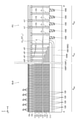
図1は、本実施形態に係る半導体記憶装置の模式的な平面図である。図1に示す様に、本実施形態に係る半導体記憶装置は、半導体基板100を備える。図示の例において、半導体基板100にはX方向に並ぶ2つのメモリセルアレイ領域RMCAが設けられる。また、メモリセルアレイ領域RMCAには、メモリホール領域RMHと、メモリホール領域RMHとX方向に並ぶ位置に設けられたフックアップ領域RHUと、が設けられている。フックアップ領域RHUは、メモリホール領域RMHのX方向の両端部に沿ってY方向に延伸する。また、メモリセルアレイ領域RMCAとX方向に並ぶ位置には、ロウデコーダ領域RRDが設けられている。ロウデコーダ領域RRDは、メモリセルアレイ領域RMCAのX方向の両端部に沿ってY方向に延伸する。また、半導体基板100のY方向の端部には、X方向に延伸する周辺回路領域RPCが設けられている。
[First Embodiment]
[Construction]
FIG. 1 is a schematic plan view of the semiconductor storage device according to the present embodiment. As shown in FIG. 1, the semiconductor storage device according to this embodiment includes a
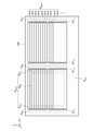
図2は、メモリセルアレイ領域RMCAの模式的な斜視図である。図2に示す様に、メモリセルアレイ領域RMCAには、Y方向に並ぶ複数のメモリブロックBLKと、Y方向において隣り合う2つのメモリブロックBLKの間にそれぞれ設けられたブロック間構造STX1と、メモリブロックBLKの上方に配置され、Y方向に延伸する複数のビット線BLと、が設けられている。また、メモリセルアレイ領域RMCAとロウデコーダ領域RRDとの間の領域には、Y方向に延伸するブロック側構造STY1が設けられている。 FIG. 2 is a schematic perspective view of the memory cell array region RMCA . As shown in FIG. 2, in the memory cell array area RMCA , a plurality of memory blocks BLK arranged in the Y direction and an inter-block structure ST X1 provided between two adjacent memory blocks BLK in the Y direction, respectively. A plurality of bit lines BL arranged above the memory block BLK and extending in the Y direction are provided. Further, a block-side structure STY1 extending in the Y direction is provided in the region between the memory cell array region RMCA and the row decoder region RRD .
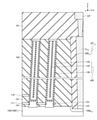
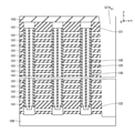
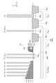
次に、図3~図10を参照して、本実施形態に係る半導体記憶装置に含まれる各構成について説明する。図3は、図1に示す構成をA-A´に沿って切断し、Y方向に沿って見た場合の模式的な断面図である。図4は、図1の一部の模式的な拡大図である。図5は、図4に示す構造をC-C´線に沿って切断し、X方向に沿って見た場合の模式的な断面図である。図6は、図5のDで示す部分の模式的な拡大図である。図7は、ロウデコーダ領域RRDに設けられたトランジスタTrの構成を示す模式的な断面図である。図8は、図3のEで示す部分の模式的な拡大図である。図9は、図8のFで示す部分を含む模式的な拡大図である。図10は、フックアップ領域RHUの一部の構成を示す模式的な断面図である。 Next, with reference to FIGS. 3 to 10, each configuration included in the semiconductor storage device according to the present embodiment will be described. FIG. 3 is a schematic cross-sectional view when the configuration shown in FIG. 1 is cut along AA'and viewed along the Y direction. FIG. 4 is a schematic enlarged view of a part of FIG. FIG. 5 is a schematic cross-sectional view when the structure shown in FIG. 4 is cut along the CC'line and viewed along the X direction. FIG. 6 is a schematic enlarged view of the portion shown by D in FIG. FIG. 7 is a schematic cross-sectional view showing the configuration of the transistor Tr provided in the row decoder region RRD . FIG. 8 is a schematic enlarged view of the portion shown by E in FIG. FIG. 9 is a schematic enlarged view including the portion shown by F in FIG. FIG. 10 is a schematic cross-sectional view showing a partial configuration of the hookup region RHU .
[半導体基板100の構造]
半導体基板100(図3)は、例えば、ホウ素(B)等のP型の不純物を含むP型のシリコン(Si)からなる半導体基板である。例えば図3に示す様に、半導体基板100の表面には、例えば、リン(P)等のN型の不純物を含むN型ウェル領域100Nと、ホウ素(B)等のP型の不純物を含むP型ウェル領域100Pと、N型ウェル領域100N及びP型ウェル領域100Pが設けられていない半導体基板領域100Sと、絶縁領域100Iと、が設けられている。尚、図示の例では、メモリセルアレイ領域RMCAにP型ウェル領域100P(以下、「P型ウェル領域100P1」と呼ぶ。)が設けられており、このP型ウェル領域100P1と半導体基板領域100Sと間にはN型ウェル領域100Nが設けられている。また、ロウデコーダ領域RRDには半導体基板領域100Sが設けられている。
[Structure of semiconductor substrate 100]
The semiconductor substrate 100 (FIG. 3) is a semiconductor substrate made of P-type silicon (Si) containing P-type impurities such as boron (B). For example, as shown in FIG. 3, the surface of the
[メモリブロックBLKのメモリホール領域RMHにおける構造]
メモリブロックBLKのメモリホール領域RMHには、Z方向に並ぶ複数の導電層110と、Z方向に延伸する複数の半導体層120と、複数の導電層110及び複数の半導体層120の間にそれぞれ設けられた複数のゲート絶縁膜130(図5)と、が設けられている。
[Structure of memory block BLK in memory hole area RMH ]
In the memory hole region RMH of the memory block BLK, between the plurality of
導電層110は、X方向に延伸する略板状の導電層である。導電層110は、窒化チタン(TiN)等のバリア導電膜及びタングステン(W)等の金属膜の積層膜等を含んでいても良い。また、導電層110は、例えば、リン(P)又はホウ素(B)等の不純物を含む多結晶シリコン等を含んでいても良い。Z方向に並ぶ複数の導電層110の間には、酸化シリコン(SiO2)等の絶縁層101が設けられている。複数の導電層110のうちの一部は、ワード線及びこれに接続された複数のメモリセルのゲート電極として機能する。また、複数の導電層110のうちの一部は、選択ゲート線及びこれに接続された選択ゲートトランジスタのゲート電極として機能する。
The
導電層110の下方には、導電層111が設けられている。導電層111は、例えば、窒化チタン(TiN)等のバリア導電膜及びタングステン(W)等の金属膜の積層膜等を含んでいても良い。また、導電層111及び導電層110の間には、酸化シリコン(SiO2)等の絶縁層101が設けられている。導電層111は、選択ゲート線及びこれに接続された選択ゲートトランジスタのゲート電極として機能する。
Below the
半導体層120は、例えば図4に示す様に、X方向及びY方向に所定のパターンで並ぶ。半導体層120は、Z方向に並ぶ複数のメモリセル及び選択ゲートトランジスタのチャネル領域として機能する。半導体層120は、例えば、多結晶シリコン(Si)等の半導体層である。半導体層120は、例えば図5に示す様に、略有底円筒状の形状を有し、中心部分には酸化シリコン等の絶縁層125が設けられている。また、半導体層120の外周面は、それぞれ導電層110によって囲われており、導電層110と対向している。
As shown in FIG. 4, for example, the semiconductor layers 120 are arranged in a predetermined pattern in the X direction and the Y direction. The
半導体層120の上端部には、リン(P)等のN型の不純物を含む不純物領域121が設けられている。不純物領域121は、コンタクトCh及びコンタクトCbを介し、X方向に並ぶ複数のビット線BLにそれぞれ接続される(図4参照)。
An
半導体層120の下端部は、単結晶シリコン(Si)等からなる半導体層122を介して、半導体基板100のP型ウェル領域100P1に接続されている。半導体層122は、選択ゲートトランジスタのチャネル領域として機能する。半導体層122の外周面は、導電層111によって囲われており、導電層111と対向している。半導体層122と導電層111との間には、酸化シリコン等の絶縁層123が設けられている。
The lower end of the
ゲート絶縁膜130は、半導体層120の外周面を覆う略円筒状の形状を有する。
The
ゲート絶縁膜130は、例えば図6に示す様に、半導体層120及び導電層110の間に積層されたトンネル絶縁膜131、電荷蓄積膜132及びブロック絶縁膜133を備える。トンネル絶縁膜131及びブロック絶縁膜133は、例えば、酸化シリコン(SiO2)等の絶縁膜である。電荷蓄積膜132は、例えば、窒化シリコン(Si3N4)等の電荷を蓄積可能な膜である。トンネル絶縁膜131、電荷蓄積膜132、及び、ブロック絶縁膜133は略円筒状の形状を有し、半導体層120の外周面に沿ってZ方向に延伸する。
As shown in FIG. 6, for example, the
尚、図6には、ゲート絶縁膜130が窒化シリコン等の電荷蓄積膜132を備える例を示した。しかしながら、ゲート絶縁膜130は、例えば、N型又はP型の不純物を含む多結晶シリコン等のフローティングゲートを備えていても良い。
Note that FIG. 6 shows an example in which the
[メモリブロックBLKのフックアップ領域RHUにおける構造]
メモリブロックBLKのフックアップ領域RHUには、例えば図3に示す様に、複数の導電層110のX方向における端部が設けられている。これら複数の端部は、それぞれX方向における位置又はY方向における位置が異なっている。これにより、メモリブロックBLKのX方向における端部には、略階段状の構造が形成されている。
[Structure in hookup area RHU of memory block BLK]
As shown in FIG. 3, for example, the hookup region RHU of the memory block BLK is provided with end portions of a plurality of
また、フックアップ領域RHUには、例えば図4に示す様に、X方向及びY方向にマトリクス状に並ぶ複数のコンタクトCCが設けられている。図3に示す様に、これら複数のコンタクトCCはZ方向に延伸し、下端において導電層110と接続されている。また、これら複数のコンタクトCCは、上端において、上方に設けられた複数の配線m0,m1(図3)に接続されている。コンタクトCCは、例えば、窒化チタン(TiN)等のバリア導電膜及びタングステン(W)等の金属膜の積層膜等を含んでいても良い。
Further, in the hookup region RHU , for example, as shown in FIG. 4, a plurality of contact CCs arranged in a matrix in the X direction and the Y direction are provided. As shown in FIG. 3, these plurality of contact CCs extend in the Z direction and are connected to the
また、図4に示す様に、フックアップ領域RHUには、コンタクトCCの近傍に設けられた支持構造HRが設けられている。支持構造HRの外周面は、それぞれ導電層110によって囲われており、導電層110と接続されている。支持構造HRは、例えば図10に示す様に、半導体層120、絶縁層125及びゲート絶縁膜130を含んでいても良い。また、支持構造HRは、これらの構造のかわりに、略円柱状に構成された酸化シリコン(SiO2)等の絶縁層を含んでいても良い。尚、本実施形態に係る支持構造HRは、ロウデコーダ領域RRD側に傾いていても良い。即ち、支持構造HRの上端のX方向における位置は、支持構造HRの下端のX方向における位置よりも、ロウデコーダ領域RRD側に位置していても良い。また、この様な傾きの大きさ(上端位置と下端位置とのX方向における差)は、メモリホール領域RMHに設けられた半導体層120(図3)及びコンタクトCC(図3)より大きくても良い。
Further, as shown in FIG. 4, the hookup region RHU is provided with a support structure HR provided in the vicinity of the contact CC. The outer peripheral surfaces of the support structure HR are each surrounded by the
[ブロック間構造STX1の構造]
ブロック間構造STX1は、例えば図4及び図5に示す様に、Z方向及びX方向に延伸する導電層LIX1と、導電層LIX1のY方向の両側面に設けられた酸化シリコン(SiO2)等の絶縁層SWX1と、を備える。導電層LIX1の下端は、複数の導電層110及び導電層111よりも下方に位置し、半導体基板100のP型ウェル領域100P1に設けられたN型の不純物領域100nX1に接続されている。不純物領域100nX1は、ブロック間構造STX1に沿ってX方向に延伸し、リン(P)等のN型の不純物を含む。導電層LIX1の上端は、複数の導電層110よりも上方、複数のビット線BLよりも下方に位置し、Y方向に延伸する配線m0に接続されている。導電層LIX1は、例えば、窒化チタン(TiN)等のバリア導電膜及びタングステン(W)等の金属膜の積層膜等を含んでいても良いし、この様な積層膜と多結晶シリコン等の半導体層とを含んでいても良いし、多結晶シリコン等の半導体層とシリサイド等とを含んでいても良い。導電層LIX1は、例えば、ソース線の一部として機能する。即ち、導電層111に電圧が供給されると、P型ウェル領域100P1に電子のチャネル(反転層)が形成され、これによって半導体層120と導電層LIX1とが導通する。尚、ブロック間構造STX1のX方向における長さは、メモリブロックBLKのX方向における長さより大きくても良い。
[Structure of inter-block structure ST X1 ]
As shown in FIGS. 4 and 5, for example, the block-to-block structure ST X1 includes a conductive layer LI X1 extending in the Z direction and the X direction, and silicon oxide (SiO) provided on both side surfaces of the conductive layer LI X1 in the Y direction. 2 ) and the like are provided with an insulating layer SW X1 and the like. The lower end of the conductive layer LI X1 is located below the plurality of
[ロウデコーダ領域RRD及び周辺回路領域RPCにおける構造]
ロウデコーダ領域RRD(図1)には、導電層110及び導電層111に電圧を転送するロウデコーダが設けられている。周辺回路領域RPC(図1)には、メモリブロックBLK等に電圧を供給するその他の回路が設けられている。
[Structure in low decoder area RRD and peripheral circuit area RPC ]
The low decoder region RRD (FIG. 1) is provided with a low decoder that transfers a voltage to the
例えば図7に例示する様に、半導体基板100のロウデコーダ領域RRD及び周辺回路領域RPCには、ゲート絶縁膜210と、ゲート電極220と、半導体基板100及びゲート電極220に接続されたコンタクトCSと、が設けられている。
For example, as illustrated in FIG. 7, the low decoder region RRD and the peripheral circuit region RPC of the
ロウデコーダ領域RRDにおいて、半導体基板100の半導体基板領域100Sは、周辺回路PCを構成する複数のトランジスタTrのチャネル領域等として機能する。また、周辺回路領域RPCにおいて、半導体基板100のN型ウェル領域100N、P型ウェル領域100P及び半導体基板領域100Sは、それぞれ、周辺回路PCを構成する複数のトランジスタTrのチャネル領域等として機能する。
In the low decoder region RRD, the semiconductor substrate region 100S of the
ゲート絶縁膜210は、半導体基板100のN型ウェル領域100N、P型ウェル領域100P及び半導体基板領域100Sに設けられている。ゲート絶縁膜210は、例えば、酸化シリコン(SiO2)等を含む。
The
ゲート電極220は、例えば、リン(P)又はホウ素(B)等の不純物を含む多結晶シリコン等の半導体層221,222と、タングステン(W)等の導電層223と、を備える。また、ゲート電極220の上面には、例えば、窒化シリコン(SiN)等の絶縁層225が設けられている。
The
コンタクトCSは、Z方向に延伸し、下端において半導体基板100又はゲート電極220の上面に接続されている。また、図3に示す様に、コンタクトCSは、上端において、上方に設けられた複数の配線m0,m1に接続されている。コンタクトCSは、例えば、窒化チタン(TiN)等のバリア導電膜及びタングステン(W)等の金属膜の積層膜等を含んでいても良い。
The contact CS extends in the Z direction and is connected to the upper surface of the
[メモリセルアレイ領域RMCAとロウデコーダ領域RRDとの間の領域における構造]
図8に示す様に、メモリセルアレイ領域RMCAとロウデコーダ領域RRDとの間の領域には、メモリセルアレイ領域RMCA側から順に、ガードリング領域RGR1と、絶縁領域100I1と、ガードリング領域RGR2と、絶縁領域100I2と、ガードリング領域RGR3と、絶縁領域100I3と、が設けられている。
[Structure in the area between the memory cell array area RMCA and the row decoder area RRD ]
As shown in FIG. 8, in the area between the memory cell array area R MCA and the low decoder area R RD , the guard ring area R GR1 , the insulation area 100I 1 , and the guard ring are arranged in order from the memory cell array area R MCA side. The region R GR2 , the insulating region 100I 2 , the guard ring region R GR3 , and the insulating region 100I 3 are provided.
ガードリング領域RGR1は、メモリセルアレイ領域RMCAと共通のP型ウェル領域100P1に設けられ、半導体基板100の表面においてメモリセルアレイ領域RMCAを取り囲む様に形成されている。絶縁領域100I1は、ガードリング領域RGR1とガードリング領域RGR2との間に設けられ、半導体基板100の表面においてガードリング領域RGR1を取り囲む様に形成されている。
The guard ring region R GR1 is provided in the P-
ガードリング領域RGR2は、P型ウェル領域100P1と半導体基板領域100Sとの間のN型ウェル領域100Nに設けられ、半導体基板100の表面において絶縁領域100I1を取り囲む様に形成されている。また、ガードリング領域RGR2においては、半導体基板100の表面に、リン(P)等のN型の不純物を含む不純物領域100n2が設けられている。また、ガードリング領域RGR2には、この不純物領域100n2に沿って設けられた複数のコンタクトCSが設けられている。これら複数のコンタクトCSは、N型ウェル領域100Nにウェル電圧を供給する。絶縁領域100I2は、ガードリング領域RGR2とガードリング領域RGR3との間に設けられ、半導体基板100の表面においてガードリング領域RGR2を取り囲む様に形成されている。
The guard ring region R GR2 is provided in the N-
ガードリング領域RGR3は、P型ウェル領域100P1とは別に設けられたP型ウェル領域100P2に設けられ、半導体基板100の表面において絶縁領域100I2を取り囲む様に形成されている。また、ガードリング領域RGR3においては、半導体基板100の表面に、ホウ素(B)等のP型の不純物を含む不純物領域100p2が設けられている。また、ガードリング領域RGR3には、この不純物領域100p2に沿って設けられた複数のコンタクトCSが設けられている。これら複数のコンタクトCSは、P型ウェル領域100P2にウェル電圧を供給する。
The guard ring region R GR3 is provided in the P-
また、ガードリング領域RGR1とメモリセルアレイ領域RMCAとの間には、ダミートランジスタ構造DTrと、ブロック側構造STY1と、が設けられている。ダミートランジスタ構造DTrは、トランジスタTrに含まれるゲート絶縁膜210、ゲート電極220及び絶縁層225を備える。ただし、これらの構成は、トランジスタTrとしては機能しない。ブロック側構造STY1は、ダミートランジスタ構造DTrよりもメモリセルアレイ領域RMCA側に設けられている。
Further, a dummy transistor structure DTr and a block-side structure STY1 are provided between the guard ring region R GR1 and the memory cell array region R MCA . The dummy transistor structure DTr includes a
[ブロック側構造STY1の構造]
ブロック側構造STY1は、例えば図4及び図9に示す様に、Z方向及びY方向に延伸する導電層LIY1と、導電層LIY1のX方向の両側面に設けられた酸化シリコン(SiO2)等の絶縁層SWY1と、を備える。導電層LIY1の下端は、複数の導電層110及び導電層111よりも下方に位置し、半導体基板100のP型ウェル領域100P1に設けられたP型の不純物領域100pY1に接続されている。不純物領域100pY1は、ブロック側構造STY1に沿ってY方向に延伸し、ホウ素(B)等のP型の不純物を含む。導電層LIY1の上端は、複数の導電層110よりも上方、複数のビット線BLよりも下方に位置し、配線m0に接続されている。導電層LIY1は、例えば、窒化チタン(TiN)等のバリア導電膜及びタングステン(W)等の金属膜の積層膜等を含んでいても良いし、この様な積層膜と多結晶シリコン等の半導体層とを含んでいても良いし、多結晶シリコン等の半導体層とシリサイド等とを含んでいても良い。導電層LIY1は、例えば、P型ウェル領域100P1に接地電圧を供給する配線として機能しても良い。即ち、導電層LIY1は、半導体記憶装置の、接地電圧が供給される図示しない外部端子と、電気的に接続されていても良い。尚、ブロック側構造STY1は、X方向において、メモリブロックBLK及びブロック間構造STX1から離れた位置に設けられている。また、図1の例において、ブロック側構造STY1のY方向における長さは、メモリセルアレイ領域RMCAのY方向における幅と一致している。ただし、ブロック側構造STY1のY方向における長さは、メモリセルアレイ領域RMCAのY方向における幅より大きくても良いし、小さくても良い。また、図4の例において、ブロック側構造STY1のX方向における幅は、ブロック間構造STX1のY方向における幅と一致している。ただし、ブロック側構造STY1のX方向における幅は、ブロック間構造STX1のY方向における幅より大きくても良いし、小さくても良い。
[Structure of block side structure ST Y1 ]
As shown in FIGS. 4 and 9, for example, the block-side structure ST Y1 includes a conductive layer LI Y1 extending in the Z direction and the Y direction, and silicon oxide (SiO) provided on both side surfaces of the conductive layer LI Y1 in the X direction. 2 ) and the like are provided with an insulating layer SW Y1 . The lower end of the conductive layer LI Y1 is located below the plurality of
[製造方法]
次に、図11~図21を参照して、第1実施形態に係る半導体記憶装置の製造方法について説明する。図11、図13~図15、図18~図20は、同製造方法について説明するための模式的な断面図であり、図5に対応する構成を示している。図12は、同製造方法について説明するための模式的な断面図であり、図8に対応する断面を示している。図16及び図21は、同製造方法について説明するための模式的な断面図であり、図9に対応する断面を示している。図17は、同製造方法について説明するための模式的な斜視図であり、図2に対応する構成を示している。
[Production method]
Next, a method of manufacturing the semiconductor storage device according to the first embodiment will be described with reference to FIGS. 11 to 21. 11, FIGS. 13 to 15, and FIGS. 18 to 20 are schematic cross-sectional views for explaining the manufacturing method, and show a configuration corresponding to FIG. FIG. 12 is a schematic cross-sectional view for explaining the manufacturing method, and shows a cross section corresponding to FIG. 16 and 21 are schematic cross-sectional views for explaining the manufacturing method, and show a cross section corresponding to FIG. 9. FIG. 17 is a schematic perspective view for explaining the manufacturing method, and shows a configuration corresponding to FIG. 2.
本実施形態に係る半導体記憶装置の製造に際しては、まず、半導体基板100のロウデコーダ領域RRD及び周辺回路領域RPCに、周辺回路PCを構成する複数のトランジスタTr(図3)を形成する。
In manufacturing the semiconductor storage device according to the present embodiment, first, a plurality of transistors Tr (FIG. 3) constituting the peripheral circuit PC are formed in the low decoder region RRD and the peripheral circuit region RPC of the
次に、例えば図11に示す様に、半導体基板100上に、複数の犠牲層110A及び絶縁層101を形成する。犠牲層110Aは、例えば、窒化シリコン(SiN)等からなる。この工程は、例えば、CVD(Chemical Vapor Deposition)等の方法によって行う。尚、複数の犠牲層110A及び絶縁層101は、図1を参照して説明したメモリセルアレイ領域RMCAに形成される。
Next, for example, as shown in FIG. 11, a plurality of
次に、例えば図12に示す様に、フックアップ領域RHUにおいて複数の犠牲層110A及び絶縁層101の一部を除去し、略階段状の構造を形成する。この工程は、例えば、図11を参照して説明した構造の上面にレジストを形成し、RIE(Reactive Ion Etching)等による絶縁層101の除去、RIE等による犠牲層110Aの除去及びレジストの等方的な除去を繰り返すことによって行う。
Next, as shown in FIG. 12, for example, a part of the plurality of
次に、この階段状の構造を覆う絶縁層102(図9参照)を形成する。この工程は、例えば、CVD等の方法によって行う。 Next, an insulating layer 102 (see FIG. 9) covering the stepped structure is formed. This step is performed by, for example, a method such as CVD.
次に、例えば図13に示す様に、半導体層120に対応する位置、及び、支持構造HRに対応する位置に、複数のメモリホールMHを形成する。メモリホールMHは、Z方向に延伸し、絶縁層101及び犠牲層110Aを貫通し、半導体基板100の上面を露出させる貫通孔である。この工程は、例えば、RIE等の方法によって行う。
Next, for example, as shown in FIG. 13, a plurality of memory holes MH are formed at a position corresponding to the
次に、例えば図14に示す様に、メモリホールMHの内部に、半導体層122、ゲート絶縁膜130、半導体層120、及び、絶縁層125を形成する。この工程は、例えば、エピタキシャル成長、CVD、RIE等の方法によって行う。
Next, for example, as shown in FIG. 14, a
次に、例えば図15~図17に示す様に、ブロック間構造STX1に対応する位置に溝STAX1を形成し、ブロック側構造STY1に対応する位置に溝STAY1を形成する。溝STAX1は、Z方向及びX方向に延伸し、絶縁層101及び犠牲層110AをY方向に分断し、半導体基板100の上面を露出させる。溝STAY1は、Z方向及びY方向に延伸し、半導体基板100の上面を露出させる。この工程は、例えば、図14を参照して説明した構造の上面にSiO2等の絶縁層103を形成し、この絶縁層103をマスクとするRIE等を実行することによって行う。
Next, as shown in FIGS. 15 to 17, for example, the groove STA X1 is formed at a position corresponding to the inter-block structure ST X1 , and the groove STA Y1 is formed at a position corresponding to the block-side structure STY1 . The groove STA X1 extends in the Z direction and the X direction, divides the insulating
次に、例えば図18に示す様に、溝STAX1を介して犠牲層110Aを除去する。これにより、Z方向に配設された複数の絶縁層101と、この絶縁層101を支持するメモリホールMH内の構造(半導体層120、ゲート絶縁膜130及び絶縁層125)、並びに、支持構造HRを含む中空構造が形成される。この工程は、例えば、ウェットエッチング等の方法によって行う。
Next, as shown in FIG. 18, for example, the
次に、例えば図19に示す様に、絶縁層123を形成する。この工程は、例えば、酸化処理等の方法によって行う。また、導電層110及び導電層111を形成する。この工程は、例えば、CVD等の方法によって行う。
Next, for example, as shown in FIG. 19, the insulating
次に、例えば、図20に示す様に溝STAX1にブロック間構造STX1を形成し、図21に示す様に溝STAY1にブロック側構造STY1を形成する。この工程では、例えば、CVD等の方法によって、溝STAX1,溝STAY1の側壁に、酸化シリコン(SiO2)等の絶縁層を、溝STAX1,溝STAY1が埋め込まれない程度に薄く形成することにより、絶縁層SWX1,SWY1を形成する。また、例えば、RIE等の方法によって絶縁層SWX1,SWY1の半導体基板100上面を覆う部分を除去し、半導体基板100の上面を露出させる。また、例えば、半導体基板100の上面にイオンを注入して、不純物領域100nX1,100pY1を形成する。また、例えば、CVD等の方法によって溝STAX1,溝STAY1の内部に、導電層LIX1,LIY1を形成する。
Next, for example, the inter-block structure ST X1 is formed in the groove STA X1 as shown in FIG. 20, and the block-side structure ST Y1 is formed in the groove STA Y1 as shown in FIG. 21. In this step, for example, an insulating layer such as silicon oxide (SiO 2 ) is formed thinly on the side wall of the groove STA X1 and the groove STA Y1 so as not to be embedded in the groove STA X1 and the groove STA Y1 by a method such as CVD. By doing so, the insulating layers SW X1 and SW Y1 are formed. Further, for example, the portion of the insulating layers SW X1 and SW Y1 that covers the upper surface of the
その後、コンタクトCC,CS、配線m0,m1等を形成することにより、第1実施形態に係る半導体記憶装置が形成される。 After that, the semiconductor storage device according to the first embodiment is formed by forming the contacts CC, CS, wiring m0, m1 and the like.
[比較例]
次に、図22を参照して比較例に係る半導体記憶装置について説明する。比較例に係る半導体記憶装置は、基本的には、第1実施形態に係る半導体記憶装置と同様に構成されている。ただし、比較例に係る半導体記憶装置は、ブロック側構造STY1を有していない。
[Comparison example]
Next, the semiconductor storage device according to the comparative example will be described with reference to FIG. 22. The semiconductor storage device according to the comparative example is basically configured in the same manner as the semiconductor storage device according to the first embodiment. However, the semiconductor storage device according to the comparative example does not have the block-side structure STY1 .
次に、図23を参照して、比較例に係る半導体記憶装置の製造方法について説明する。比較例に係る半導体記憶装置は、基本的には、第1実施形態に係る半導体記憶装置と同様に製造される。ただし、比較例に係る製造方法においては、図23に示す様に、図15~図17を参照して説明した工程において溝STAX1のみを形成し、溝STAY1を形成しない。 Next, a method of manufacturing the semiconductor storage device according to the comparative example will be described with reference to FIG. 23. The semiconductor storage device according to the comparative example is basically manufactured in the same manner as the semiconductor storage device according to the first embodiment. However, in the manufacturing method according to the comparative example, as shown in FIG. 23, only the groove STA X1 is formed and the groove STA Y1 is not formed in the steps described with reference to FIGS. 15 to 17.
[第1実施形態の効果]
比較例に係る半導体記憶装置の製造に際しては、図18を参照して説明した工程において、例えば図24に例示する様に、複数の絶縁層101を含む中空構造が歪んでしまう場合がある。これは、フックアップ領域RHUに設けられた絶縁層102のX方向の圧縮応力によって絶縁層101がX方向中心側に向かって押圧されてしまうためと考えられる。
[Effect of the first embodiment]
In manufacturing the semiconductor storage device according to the comparative example, in the process described with reference to FIG. 18, for example, as illustrated in FIG. 24, the hollow structure including the plurality of insulating
ここで、第1実施形態に係る半導体記憶装置の製造に際しては、図17等を参照して説明した工程において、溝STAX1だけでなく、溝STAY1も形成する。従って、図25に例示する様に、絶縁層102のX方向の圧縮応力をロウデコーダ領域RRD側に逃がして、上述の様な中空構造の歪を好適に抑制することが出来る。
Here, in the manufacturing of the semiconductor storage device according to the first embodiment, not only the groove STA X1 but also the groove STA Y1 is formed in the process described with reference to FIG. 17 and the like. Therefore, as illustrated in FIG. 25, the compressive stress in the X direction of the insulating
また、例えば、溝STAX1と溝STAY1とが交わっている場合、図17等を参照して説明した工程において、これら溝STAX1,溝STAY1が交わる部分にRIEのガスが集中してしまい、この部分において半導体基板100が破壊されてしまう場合がある。そこで、第1実施形態に係る製造方法においては、溝STAY1を溝STAX1から離間させている。これにより、半導体記憶装置を好適に製造可能である。
Further, for example, when the groove STA X1 and the groove STA Y1 intersect, the RIE gas concentrates on the portion where the groove STA X1 and the groove STA Y1 intersect in the process described with reference to FIG. 17 and the like. In this portion, the
また、例えば、溝STAX1と溝STAY1とが交わっている場合、図17等を参照して説明した工程において、半導体基板100上に設けられた構造がY方向に完全に分断されてしまう。この様な場合、上記圧縮応力等に起因して各構造に歪が生じ、これら構造間のY方向における距離(溝STAX1のY方向における幅)にばらつきが生じてしまう場合がある。そこで、第1実施形態に係る製造方法においては、溝STAY1を溝STAX1から離間させている。この様な方法によれば、溝STAX1によって分断された各構造が、絶縁層102,103を介してお互いに接続された状態となる。従って、絶縁層102,103を介して各構造間の位置関係を固定して、上述の様なばらつきの発生を抑制可能である。これにより、半導体記憶装置を好適に製造可能である。
Further, for example, when the groove STA X1 and the groove STA Y1 intersect, the structure provided on the
また、上述の様に溝STAY1によって絶縁層102のX方向の圧縮応力をロウデコーダ領域RRD側に逃がそうとする場合、溝STAY1は、メモリセルアレイ領域RMCAの近傍に設けることが望ましい。溝STAY1とメモリセルアレイ領域RMCAとの距離が近いほど、絶縁層102のX方向における幅が小さくなり、絶縁層102がX方向において変形しやすくなるためである。そこで、図8を参照して説明した様に、第1実施形態においては、溝STAY1を、ガードリング領域RGR1よりも内側に配置している。これにより、上述の様な中空構造の歪を好適に抑制することが出来る。
Further, when the compression stress in the X direction of the insulating
また、図9等を参照して説明した様に、本実施形態に係る導電層LIY1はY方向に並ぶ複数のメモリブロックBLKに沿ってY方向に延伸し、且つ、接地電圧が供給されている。この様な構成においては、導電層LIY1がシールド電極として機能するため、メモリブロックBLKを外部の電磁波から保護することが可能である。 Further, as described with reference to FIG. 9 and the like, the conductive layer LI Y1 according to the present embodiment is extended in the Y direction along a plurality of memory blocks BLK arranged in the Y direction, and a ground voltage is supplied. There is. In such a configuration, since the conductive layer LI Y1 functions as a shield electrode, it is possible to protect the memory block BLK from external electromagnetic waves.
[第2実施形態]
次に、図26及び図27を参照して、第2実施形態に係る半導体記憶装置について説明する。第2実施形態に係る半導体記憶装置は、基本的には第1実施形態に係る半導体記憶装置と同様に構成されている。ただし、図2等に示す様に、第1実施形態に係る半導体記憶装置においては、メモリセルアレイ領域RMCAのX方向の両側に、1本ずつブロック側構造STY1が設けられていた。一方、図26に示す様に、第2実施形態においては、メモリセルアレイ領域RMCAのX方向の両側に、2本ずつブロック側構造STY1が設けられている。また、図27に示す様に、これら2本のブロック側構造STY1は、どちらもダミートランジスタ構造DTrよりメモリセルアレイ領域RMCA側に設けられている。
[Second Embodiment]
Next, the semiconductor storage device according to the second embodiment will be described with reference to FIGS. 26 and 27. The semiconductor storage device according to the second embodiment is basically configured in the same manner as the semiconductor storage device according to the first embodiment. However, as shown in FIG. 2 and the like, in the semiconductor storage device according to the first embodiment, one block-side structure STY1 is provided on both sides of the memory cell array region RMCA in the X direction. On the other hand, as shown in FIG. 26, in the second embodiment, two block-side structures STY1 are provided on both sides of the memory cell array region RMCA in the X direction. Further, as shown in FIG. 27, both of these two block-side structures STY1 are provided on the memory cell array region RMCA side of the dummy transistor structure DTr.
この様な構成においては、メモリセルアレイ領域RMCA近傍に設けられた2つの導電層LIY1がどちらもシールド電極として機能するため、メモリブロックBLKを外部の電磁波からより好適に保護することが可能である。 In such a configuration, since the two conductive layers LI Y1 provided in the vicinity of the memory cell array region RMCA both function as shield electrodes, it is possible to more preferably protect the memory block BLK from external electromagnetic waves. be.
[第3実施形態]
次に、図28及び図29を参照して、第3実施形態に係る半導体記憶装置について説明する。第3実施形態に係る半導体記憶装置は、基本的には第2実施形態に係る半導体記憶装置と同様に構成されている。ただし、図26に示す様に、第2実施形態に係る半導体記憶装置においては、メモリセルアレイ領域RMCAのX方向の両側に、2本ずつブロック側構造STY1が設けられていた。一方、図28に示す様に、第3実施形態においては、メモリセルアレイ領域RMCAのX方向の両側に、2本のブロック側構造STY1に加え、更に1本ずつブロック側構造STY3が設けられている。また、図29に示す様に、ブロック側構造STY3は、ガードリング領域RGR2に設けられている。
[Third Embodiment]
Next, the semiconductor storage device according to the third embodiment will be described with reference to FIGS. 28 and 29. The semiconductor storage device according to the third embodiment is basically configured in the same manner as the semiconductor storage device according to the second embodiment. However, as shown in FIG. 26, in the semiconductor storage device according to the second embodiment, two block-side structures STY1 are provided on both sides of the memory cell array region RMCA in the X direction. On the other hand, as shown in FIG. 28, in the third embodiment, in addition to the two block-side structures STY1 on both sides of the memory cell array region RMCA in the X direction, one block-side structure STY3 is provided. Has been done. Further, as shown in FIG. 29, the block-side structure STY3 is provided in the guard ring region RGR2 .
ブロック側構造STY3は、基本的にはブロック側構造STY1と同様に構成されている。ただし、ブロック側構造STY1に含まれる導電層LIY1は、P型の不純物領域100pY1を介して、P型ウェル領域100P1に接続されていた。一方、ブロック側構造STY3に含まれる導電層LIY3は、不純物領域100n2を介して、N型ウェル領域100Nに接続されている。
The block-side structure STY3 is basically configured in the same manner as the block-side structure STY1 . However, the conductive layer LI Y1 included in the block-side structure ST Y1 was connected to the P-
この様な構成においては、メモリセルアレイ領域RMCA近傍に設けられた2つの導電層LIY1及び導電層LIY3が全てシールド電極として機能するため、メモリブロックBLKを外部の電磁波からより好適に保護することが可能である。 In such a configuration, since the two conductive layers LI Y1 and the conductive layer LI Y3 provided in the vicinity of the memory cell array region RMCA all function as shield electrodes, the memory block BLK is more preferably protected from external electromagnetic waves. It is possible.
[第4実施形態]
次に、図30を参照して、第4実施形態に係る半導体記憶装置について説明する。第4実施形態に係る半導体記憶装置は、基本的には第1実施形態に係る半導体記憶装置と同様に構成されている。ただし、図2等に示す様に、第1実施形態に係る半導体記憶装置においては、メモリセルアレイ領域RMCAのX方向の両側に、1本ずつブロック側構造STY1が設けられていた。一方、図26に示す様に、第2実施形態においては、メモリセルアレイ領域RMCAのX方向の両側に、更に1本ずつブロック側構造STY4が設けられている。また、図30に示す様に、ブロック側構造STY4は、ダミートランジスタ構造DTrとブロック側構造STY1との間に設けられている。
[Fourth Embodiment]
Next, the semiconductor storage device according to the fourth embodiment will be described with reference to FIG. 30. The semiconductor storage device according to the fourth embodiment is basically configured in the same manner as the semiconductor storage device according to the first embodiment. However, as shown in FIG. 2 and the like, in the semiconductor storage device according to the first embodiment, one block-side structure STY1 is provided on both sides of the memory cell array region RMCA in the X direction. On the other hand, as shown in FIG. 26, in the second embodiment, block-side structures STY4 are further provided on both sides of the memory cell array region RMCA in the X direction. Further, as shown in FIG. 30, the block-side structure STY4 is provided between the dummy transistor structure DTr and the block-side structure STY1 .
ブロック側構造STY4は、基本的にはブロック側構造STY1と同様に構成されている。ただし、ブロック側構造STY4の下方には、ダミートランジスタ構造DTr´が設けられている。ダミートランジスタ構造DTr´は、ダミートランジスタ構造DTrと同様に構成されている。また、ブロック側構造STY4に含まれる導電層LIY4の下端は、このダミートランジスタ構造DTr´に含まれる導電層223の上面に接続されている。
The block-side structure STY4 is basically configured in the same manner as the block-side structure STY1 . However, a dummy transistor structure DTr'is provided below the block-side structure STY4 . The dummy transistor structure DTr'is configured in the same manner as the dummy transistor structure DTr. Further, the lower end of the conductive layer LI Y4 included in the block-side structure STY4 is connected to the upper surface of the
この様な構成においても、メモリセルアレイ領域RMCA近傍に設けられた導電層LIY1及び導電層LIY4がどちらもシールド電極として機能するため、メモリブロックBLKを外部の電磁波からより好適に保護することが可能である。 Even in such a configuration, since both the conductive layer LI Y1 and the conductive layer LI Y4 provided in the vicinity of the memory cell array region RMCA function as shield electrodes, the memory block BLK should be more preferably protected from external electromagnetic waves. Is possible.
[第5実施形態]
次に、図31及び図32を参照して、第5実施形態に係る半導体記憶装置について説明する。第5実施形態に係る半導体記憶装置は、基本的には第1実施形態に係る半導体記憶装置と同様に構成されている。ただし、第5実施形態に係る半導体記憶装置は、ブロック側構造STY1のかわりに、ブロック側構造STY5を備えている。
[Fifth Embodiment]
Next, the semiconductor storage device according to the fifth embodiment will be described with reference to FIGS. 31 and 32. The semiconductor storage device according to the fifth embodiment is basically configured in the same manner as the semiconductor storage device according to the first embodiment. However, the semiconductor storage device according to the fifth embodiment includes the block-side structure STY5 instead of the block-side structure STY1 .
ブロック側構造STY5は、基本的にはブロック側構造STY1と同様に構成されている。ただし、図4、図10等を参照して説明した様に、第1実施形態に係るブロック側構造STY1は、導電層LIY1を備えていた。一方、図31及び図32に示す様に、第5実施形態に係るブロック側構造STY5は、導電層LIY1を備えておらず、酸化シリコン(SiO2)等の絶縁層によって構成されている。また、図31に示す様に、ブロック側構造STY4のX方向における幅WSTY5は、ブロック間構造STX1に含まれる絶縁層SWX1のY方向における幅WSWX1の倍の幅2WSWX1以下の大きさを有する。 The block-side structure STY5 is basically configured in the same manner as the block-side structure STY1 . However, as described with reference to FIGS. 4, 10 and the like, the block-side structure ST Y1 according to the first embodiment includes the conductive layer LI Y1 . On the other hand, as shown in FIGS. 31 and 32, the block-side structure STY5 according to the fifth embodiment does not include the conductive layer LI Y1 and is composed of an insulating layer such as silicon oxide (SiO 2 ). .. Further, as shown in FIG. 31, the width W STY5 of the block-side structure ST Y4 in the X direction is 2 W SWX1 or less, which is twice the width W SWX1 of the insulating layer SW X1 included in the inter-block structure ST X1 in the Y direction. Has a size.
第5実施形態に係る半導体記憶装置は、基本的には第1実施形態に係る半導体記憶装置と同様に製造される。ただし、第5実施形態に係る製造方法においては、図15~図17を参照して説明した工程において、溝STAY1のX方向における幅を、溝STAX1のY方向における幅よりも小さくする。また、図20を参照して説明した工程において絶縁層SWX1を形成する際、この絶縁層SWX1によって溝STAX1が埋め込まれず、且つ、溝STAY1が埋め込まれる程度の膜厚で、酸化シリコン(SiO2)等の絶縁層を形成する。 The semiconductor storage device according to the fifth embodiment is basically manufactured in the same manner as the semiconductor storage device according to the first embodiment. However, in the manufacturing method according to the fifth embodiment, in the steps described with reference to FIGS. 15 to 17, the width of the groove STA Y1 in the X direction is made smaller than the width of the groove STA X1 in the Y direction. Further, when the insulating layer SW X1 is formed in the process described with reference to FIG. 20, the silicon oxide has a thickness such that the groove STA X1 is not embedded by the insulating layer SW X1 and the groove STA Y1 is embedded. An insulating layer such as (SiO 2 ) is formed.
この様な構成によれば、より少ない面積によって、上述の様な中空構造の歪を抑制することが出来る。 According to such a configuration, it is possible to suppress the distortion of the hollow structure as described above with a smaller area.
尚、図32の例では、ブロック側構造STY5の下端が半導体基板100の上面に達している例を示した。しかしながら、例えば図33に示す様に、ブロック側構造STY5の下端は、半導体基板100の上面、導電層111及び一部の導電層110よりも上方に位置してしても良い。
In the example of FIG. 32, an example is shown in which the lower end of the block-side structure STY5 reaches the upper surface of the
[第6実施形態]
次に、図34及び図35を参照して、第6実施形態に係る半導体記憶装置について説明する。第6実施形態に係る半導体記憶装置は、基本的には第1実施形態に係る半導体記憶装置と同様に構成されている。
[Sixth Embodiment]
Next, the semiconductor storage device according to the sixth embodiment will be described with reference to FIGS. 34 and 35. The semiconductor storage device according to the sixth embodiment is basically configured in the same manner as the semiconductor storage device according to the first embodiment.
ただし、第6実施形態に係る半導体記憶装置は、ブロック間構造STX1のかわりに、ブロック間構造STX6を備えている。ブロック間構造STX6は、基本的にはブロック間構造STX1と同様に構成されている。ただし、図5等を参照して説明した様に、第1実施形態に係るブロック間構造STX1は、導電層LIX1を備えていた。一方、図34及び図35に示す様に、第6実施形態に係るブロック間構造STX6は、導電層LIX1を備えておらず、酸化シリコン(SiO2)等によって構成されている。また、図34に示す様に、ブロック間構造STX6のY方向における幅WSTX6は、ブロック側構造STY1に含まれる絶縁層SWY1のX方向における幅WSWY1の倍の幅2WSWY1以下の大きさを有する。 However, the semiconductor storage device according to the sixth embodiment includes the inter-block structure ST X6 instead of the inter-block structure ST X1 . The inter-block structure ST X6 is basically configured in the same manner as the inter-block structure ST X1 . However, as described with reference to FIG. 5 and the like, the inter-block structure ST X1 according to the first embodiment includes the conductive layer LI X1 . On the other hand, as shown in FIGS. 34 and 35, the inter-block structure ST X6 according to the sixth embodiment does not include the conductive layer LI X1 and is composed of silicon oxide (SiO 2 ) or the like. Further, as shown in FIG. 34, the width W STX6 of the inter-block structure ST X6 in the Y direction is 2W SWY1 or less, which is twice the width W SWY1 of the insulating layer SWY1 included in the block-side structure STY1 in the X direction. Has a size.
また、図35に示す様に、第6実施形態に係る半導体記憶装置は、半導体基板100から離間して半導体基板100の上方に設けられた半導体層140及び導電層141を備えている。半導体層140は、リン(P)等のN型の不純物を含む多結晶シリコン等の半導体層である。導電層141は、半導体層140の下面に接続されている。導電層141は、例えば、タングステン(W)等の金属であっても良いし、タングステンシリサイド等であっても良いし、その他の導電層であっても良い。また、本実施形態に係る半導体層120´は、基本的には半導体層120と同様に構成されているが、半導体基板100のP型ウェル領域100Pではなく、N型ウェル領域100Nに接続されている。
Further, as shown in FIG. 35, the semiconductor storage device according to the sixth embodiment includes a
また、第6実施形態に係る半導体記憶装置においては、ブロック側構造STY1が、Z方向から見て導電層141と重なる位置に設けられている。また、ブロック側構造STY1の下端が、半導体層140に接続されている。
Further, in the semiconductor storage device according to the sixth embodiment, the block-side structure STY1 is provided at a position overlapping with the
[その他の実施形態]
以上、第1実施形態~第6実施形態に係る半導体記憶装置について例示した。しかしながら、以上の構成及び製造方法は例示に過ぎず、具体的な構成等は、適宜調整可能である。
[Other embodiments]
The semiconductor storage devices according to the first to sixth embodiments have been illustrated above. However, the above configuration and manufacturing method are merely examples, and the specific configuration and the like can be appropriately adjusted.
例えば、第1実施形態~第5実施形態に係る半導体層120の下端は、半導体基板100のP型ウェル領域100P1に接続されていた。しかしながら、この様な構成は例示に過ぎず、具体的な構成は適宜調整可能である。例えば、半導体層120の下端は、N型ウェル領域100Nに接続されても良い。例えば、第6実施形態において例示した様に、半導体基板100の上方に、リン(P)等のN型の不純物又はホウ素(B)等のP型の不純物を含む多結晶シリコン等の半導体層を設け、半導体層120の下端を、この半導体層に接続しても良い。この様な場合、ブロック側構造STY1,STY3,STY4,STY5は、Z方向から見てP型ウェル領域100P1と重なる位置ではなく、Z方向から見て半導体層と重なる位置に設けられても良い。また、この様な場合、ブロック間構造STX1,STX6の下端、及び、ブロック側構造STY1,STY3,STY4,STY5の下端は、半導体基板100の表面ではなく、この半導体層に接続されても良い。
For example, the lower end of the
また、各実施形態に係る半導体記憶装置は、ブロック側構造STY1,STY3,STY4,STY5の少なくとも一つを備えていれば良い。例えば、第1実施形態に係る半導体記憶装置は、ブロック側構造STY1のかわりに、ブロック側構造STY3又はブロック側構造STY4を備えていても良い。また、例えば、第6実施形態に係る半導体記憶装置は、ブロック側構造STY1に加え、又は、ブロック側構造STY1のかわりに、ブロック側構造STY5を備えていても良い。尚、この様な場合、ブロック側構造STY5のX方向における幅は、ブロック間構造STX6のY方向における幅WSTX6と同程度であっても良いし、幅WSTX6より小さくても良い。 Further, the semiconductor storage device according to each embodiment may include at least one of the block-side structures STY1 , STY3 , STY4 , and STY5 . For example, the semiconductor storage device according to the first embodiment may include a block-side structure STY3 or a block-side structure STY4 instead of the block-side structure STY1 . Further, for example, the semiconductor storage device according to the sixth embodiment may include a block-side structure STY5 in addition to the block-side structure STY1 or instead of the block-side structure STY1 . In such a case, the width of the block-side structure ST Y5 in the X direction may be about the same as the width W STX 6 in the Y direction of the inter-block structure ST X 6 , or may be smaller than the width W STX 6 .
また、図1の例では、ブロック側構造STY1のY方向における長さが、メモリセルアレイ領域RMCAのY方向における長さと一致していた。しかしながら、この様な構成は例示に過ぎず、具体的な構成は適宜調整可能である。例えば図36に示す様に、ブロック側構造STY1のY方向における長さをメモリセルアレイ領域RMCAのY方向における長さよりも小さくして、ブロック側構造STY1をY方向に複数設けても良い。この様な場合、例えば、ブロック側構造STY1のY方向における長さは、一又は複数のメモリブロックBLKのY方向における幅と一致しても良いし、この様な幅より大きくても良い。その他の実施形態に係るブロック側構造STY3,STY4,STY5についても同様である。 Further, in the example of FIG. 1, the length of the block-side structure STY1 in the Y direction coincided with the length of the memory cell array region RMCA in the Y direction. However, such a configuration is merely an example, and the specific configuration can be adjusted as appropriate. For example, as shown in FIG. 36, the length of the block-side structure STY1 in the Y-direction may be made smaller than the length of the memory cell array region RMCA in the Y-direction, and a plurality of block-side structures STY1 may be provided in the Y-direction. .. In such a case, for example, the length of the block-side structure ST Y1 in the Y direction may match the width of one or more memory blocks BLK in the Y direction, or may be larger than such a width. The same applies to the block-side structures STY3 , STY4 , and STY5 according to other embodiments.
また、上述の例では、ブロック側構造STY1,STY3,STY4,STY5がZ方向及びY方向に延伸する略板状の形状を備えていた。しかしながら、例えば、これらのブロック側構造は、例えば図37に例示する様に、略円柱状に形成されていても良い。この様な場合、メモリセルアレイ領域RMCAとロウデコーダ領域RRDとの間の領域には、Y方向に並ぶ複数のブロック側構造STY1´が設けられる。尚、図37に例示するブロック側構造STY1´は、導電層LIY1´と、絶縁層SWY1´と、を備える。導電層LIY1´は、基本的には導電層LIY1と同様に構成されているが、Z方向に延伸する略円柱状に構成されている。絶縁層SWY1´は、基本的には絶縁層SWY1と同様に構成されているが、導電層LIY1´の外周面を覆う略円柱状に構成されている。尚、図37には、ブロック側構造STY1を略円柱状に構成した例を示した。しかしながら、例えば、その他の実施形態に係るブロック側構造STY3,STY4,STY5を略円柱状に構成することも可能である。 Further, in the above-mentioned example, the block-side structures STY1 , STY3 , STY4 , and STY5 have a substantially plate-like shape extending in the Z direction and the Y direction. However, for example, these block-side structures may be formed in a substantially columnar shape, as illustrated in FIG. 37, for example. In such a case, a plurality of block-side structures STY1'arranged in the Y direction are provided in the area between the memory cell array area RMCA and the low decoder area RRD . The block-side structure ST Y1 ′ exemplified in FIG. 37 includes a conductive layer LI Y1 ′ and an insulating layer SW Y1 ′. The conductive layer LI Y1 ′ is basically configured in the same manner as the conductive layer LI Y1 , but is configured in a substantially columnar shape extending in the Z direction. The insulating layer SW Y1 ′ is basically configured in the same manner as the insulating layer SW Y1 ′, but is configured in a substantially columnar shape covering the outer peripheral surface of the conductive layer LI Y1 ′. Note that FIG. 37 shows an example in which the block-side structure STY1 is configured in a substantially columnar shape. However, for example, the block-side structures STY3 , STY4 , and STY5 according to other embodiments can be configured in a substantially columnar shape.
[その他]
本発明のいくつかの実施形態を説明したが、これらの実施形態は例として提示したものであり、発明の範囲を限定することは意図していない。これら新規な実施形態は、その他の様々な形態で実施されることが可能であり、発明の要旨を逸脱しない範囲で、種々の省略、置き換え、変更を行うことが出来る。これら実施形態やその変形は、発明の範囲や要旨に含まれると共に、特許請求の範囲に記載された発明とその均等の範囲に含まれる。
[others]
Although some embodiments of the present invention have been described, these embodiments are presented as examples and are not intended to limit the scope of the invention. These novel embodiments can be implemented in various other embodiments, and various omissions, replacements, and changes can be made without departing from the gist of the invention. These embodiments and variations thereof are included in the scope and gist of the invention, and are also included in the scope of the invention described in the claims and the equivalent scope thereof.
100…半導体基板、110…導電層、120…半導体層、130…ゲート絶縁膜、BLK…メモリブロック、STX1…メモリブロック間構造、STY1…メモリブロック側構造、BL…ビット線。 100 ... semiconductor substrate, 110 ... conductive layer, 120 ... semiconductor layer, 130 ... gate insulating film, BLK ... memory block, ST X1 ... memory block inter-structure, STY1 ... memory block side structure, BL ... bit line.
Claims (13)
前記第1方向において隣り合う2つのメモリブロックの間にそれぞれ設けられ、前記第2方向に延伸する複数の第1構造と、
前記第2方向において前記複数のメモリブロックから離れ、前記第1方向に延伸し、又は、前記第1方向に複数配置された第2構造と、
前記第2方向に並び、前記第1方向に延伸し、前記複数のメモリブロックに接続された複数のビット線と
を備え、
前記複数のメモリブロックは、基板の表面と交差する第3方向に並ぶ複数の第1導電層を備え、
前記第1構造の前記第3方向における一端は、前記複数の第1導電層よりも前記基板に近く、
前記第2構造の前記第3方向における一端は、前記複数の第1導電層のうち少なくとも一部の第1導電層よりも前記基板に近く、
前記第1構造の前記第3方向における他端、及び、前記第2構造の前記第3方向における他端は、前記複数の第1導電層よりも前記基板から遠く、前記複数のビット線よりも前記基板に近く、
前記第2構造は、前記第2方向において、前記第1構造から離れている
半導体記憶装置。 A plurality of memory blocks arranged in the first direction and extending in the second direction intersecting the first direction,
A plurality of first structures provided between two adjacent memory blocks in the first direction and extending in the second direction, and a plurality of first structures.
A second structure separated from the plurality of memory blocks in the second direction, extended in the first direction, or arranged in the first direction.
It comprises a plurality of bit lines aligned in the second direction, stretched in the first direction, and connected to the plurality of memory blocks.
The plurality of memory blocks include a plurality of first conductive layers arranged in a third direction intersecting the surface of the substrate.
One end of the first structure in the third direction is closer to the substrate than the plurality of first conductive layers.
One end of the second structure in the third direction is closer to the substrate than at least a part of the first conductive layer among the plurality of first conductive layers.
The other end of the first structure in the third direction and the other end of the second structure in the third direction are farther from the substrate than the plurality of first conductive layers and more than the plurality of bit wires. Close to the board,
The second structure is a semiconductor storage device that is separated from the first structure in the second direction.
請求項1記載の半導体記憶装置。 The semiconductor storage device according to claim 1, wherein the length of the second structure in the first direction is larger than the width of at least one of the plurality of memory blocks in the first direction.
請求項1又は2記載の半導体記憶装置。 The semiconductor storage device according to claim 1 or 2, wherein the width of the second structure in the second direction is smaller than the width of the first structure in the first direction.
請求項3記載の半導体記憶装置。 The semiconductor storage device according to claim 3, wherein one end of the second structure in the third direction is farther from the substrate than the first conductive layer closest to the substrate among the plurality of first conductive layers.
請求項1又は2記載の半導体記憶装置。 The semiconductor storage device according to claim 1 or 2, wherein the width of the second structure in the second direction is larger than the width of the first structure in the first direction.
請求項1、2及び4のいずれか1項記載の半導体記憶装置。 The semiconductor storage device according to any one of claims 1, 2 and 4, wherein the second structure includes a second conductive layer extending in the first direction.
請求項6記載の半導体記憶装置。 The semiconductor storage device according to claim 6, wherein the second conductive layer is electrically connected to an external terminal capable of supplying a ground voltage.
前記複数のメモリブロックは、前記第1ウェル領域に接続され、
前記第2構造は、前記第3方向から見て、前記第1ウェル領域と重なる位置に設けられている
請求項1又は2記載の半導体記憶装置。 The substrate comprises a first well region.
The plurality of memory blocks are connected to the first well area, and the plurality of memory blocks are connected to the first well area.
The semiconductor storage device according to claim 1 or 2, wherein the second structure is provided at a position overlapping the first well region when viewed from the third direction.
前記第2導電層は、前記第1ウェル領域に接続されている
請求項8記載の半導体記憶装置。 The second structure comprises a second conductive layer extending in the first direction.
The semiconductor storage device according to claim 8, wherein the second conductive layer is connected to the first well region.
前記半導体記憶装置は、
前記基板の表面に設けられた第1絶縁層と、
前記第1絶縁層の表面に設けられた第1半導体層と、
前記第1半導体層の表面に設けられた第3導電層と
を備え、
前記第2導電層は、前記第3導電層に接続されている
請求項8記載の半導体記憶装置。 The second structure comprises a second conductive layer extending in the first direction.
The semiconductor storage device is
The first insulating layer provided on the surface of the substrate and
The first semiconductor layer provided on the surface of the first insulating layer and
A third conductive layer provided on the surface of the first semiconductor layer is provided.
The semiconductor storage device according to claim 8, wherein the second conductive layer is connected to the third conductive layer.
前記第3構造は、前記第1方向に延伸する第4導電層を備え、
前記基板は第2ウェル領域を備え、
前記第1ウェル領域は、前記第2ウェル領域に設けられ、
前記第4導電層は、前記第2ウェル領域に接続されている
請求項8~10のいずれか1項記載の半導体記憶装置。 The semiconductor storage device includes a third structure that is separated from the plurality of memory blocks in the second direction, extends in the first direction, or is arranged in a plurality in the first direction.
The third structure comprises a fourth conductive layer extending in the first direction.
The substrate comprises a second well region.
The first well region is provided in the second well region.
The semiconductor storage device according to any one of claims 8 to 10, wherein the fourth conductive layer is connected to the second well region.
前記複数のメモリブロックは、前記第2半導体層に接続され、
前記第2構造は、前記第3方向から見て、前記第2半導体層と重なる位置に設けられている
請求項1又は2記載の半導体記憶装置。 A second semiconductor layer provided between the substrate and the plurality of memory blocks is provided.
The plurality of memory blocks are connected to the second semiconductor layer, and the plurality of memory blocks are connected to the second semiconductor layer.
The semiconductor storage device according to claim 1 or 2, wherein the second structure is provided at a position overlapping the second semiconductor layer when viewed from the third direction.
前記第2導電層は、前記第2半導体層に接続されている
請求項12記載の半導体記憶装置。 The second structure comprises a second conductive layer extending in the first direction.
The semiconductor storage device according to claim 12, wherein the second conductive layer is connected to the second semiconductor layer.
Priority Applications (4)
| Application Number | Priority Date | Filing Date | Title |
|---|---|---|---|
| JP2020116116A JP2022014007A (en) | 2020-07-06 | 2020-07-06 | Semiconductor storage device |
| US17/120,341 US11756898B2 (en) | 2020-07-06 | 2020-12-14 | Semiconductor memory device |
| TW110106477A TWI750039B (en) | 2020-07-06 | 2021-02-24 | Semiconductor memory device |
| CN202110208577.1A CN113903743B (en) | 2020-07-06 | 2021-02-24 | semiconductor memory devices |
Applications Claiming Priority (1)
| Application Number | Priority Date | Filing Date | Title |
|---|---|---|---|
| JP2020116116A JP2022014007A (en) | 2020-07-06 | 2020-07-06 | Semiconductor storage device |
Publications (1)
| Publication Number | Publication Date |
|---|---|
| JP2022014007A true JP2022014007A (en) | 2022-01-19 |
Family
ID=79167202
Family Applications (1)
| Application Number | Title | Priority Date | Filing Date |
|---|---|---|---|
| JP2020116116A Pending JP2022014007A (en) | 2020-07-06 | 2020-07-06 | Semiconductor storage device |
Country Status (4)
| Country | Link |
|---|---|
| US (1) | US11756898B2 (en) |
| JP (1) | JP2022014007A (en) |
| CN (1) | CN113903743B (en) |
| TW (1) | TWI750039B (en) |
Families Citing this family (3)
| Publication number | Priority date | Publication date | Assignee | Title |
|---|---|---|---|---|
| KR102812212B1 (en) * | 2020-05-19 | 2025-05-26 | 에스케이하이닉스 주식회사 | 3 Dimensional Semiconductor Memory Device |
| JP2022050148A (en) * | 2020-09-17 | 2022-03-30 | キオクシア株式会社 | Semiconductor storage device |
| CN115996570B (en) * | 2023-03-24 | 2023-06-16 | 北京超弦存储器研究院 | Memory, manufacturing method of memory and electronic equipment |
Family Cites Families (14)
| Publication number | Priority date | Publication date | Assignee | Title |
|---|---|---|---|---|
| KR20140020628A (en) * | 2012-08-10 | 2014-02-19 | 에스케이하이닉스 주식회사 | Semiconductor memory device |
| US9502471B1 (en) * | 2015-08-25 | 2016-11-22 | Sandisk Technologies Llc | Multi tier three-dimensional memory devices including vertically shared bit lines |
| JP6581019B2 (en) | 2016-03-02 | 2019-09-25 | 東芝メモリ株式会社 | Semiconductor memory device |
| US10141327B2 (en) * | 2016-03-18 | 2018-11-27 | Toshiba Memory Corporation | Semiconductor memory device |
| JP2017195275A (en) | 2016-04-20 | 2017-10-26 | 東芝メモリ株式会社 | Semiconductor memory device and manufacturing method thereof |
| JP2018157096A (en) | 2017-03-17 | 2018-10-04 | 東芝メモリ株式会社 | Semiconductor device |
| KR102534838B1 (en) * | 2017-12-20 | 2023-05-22 | 삼성전자주식회사 | Memory device with three dimentional structure |
| JP7013293B2 (en) * | 2018-03-19 | 2022-01-31 | キオクシア株式会社 | Semiconductor storage device |
| JP2019169600A (en) | 2018-03-23 | 2019-10-03 | 東芝メモリ株式会社 | Semiconductor device and method for manufacturing the same |
| KR102612021B1 (en) * | 2018-04-03 | 2023-12-11 | 삼성전자주식회사 | Three dimensional semiconductor memory device |
| KR102714981B1 (en) * | 2019-01-18 | 2024-10-10 | 삼성전자주식회사 | Integrated circuit chip, and integrated circuit package and display apparatus including integrated circuit chip |
| JP2020126938A (en) | 2019-02-05 | 2020-08-20 | キオクシア株式会社 | Semiconductor storage device |
| JP2021034643A (en) * | 2019-08-28 | 2021-03-01 | キオクシア株式会社 | Semiconductor storage device and method for manufacturing the same |
| JP2021136353A (en) | 2020-02-27 | 2021-09-13 | キオクシア株式会社 | Semiconductor storage device |
-
2020
- 2020-07-06 JP JP2020116116A patent/JP2022014007A/en active Pending
- 2020-12-14 US US17/120,341 patent/US11756898B2/en active Active
-
2021
- 2021-02-24 CN CN202110208577.1A patent/CN113903743B/en active Active
- 2021-02-24 TW TW110106477A patent/TWI750039B/en active
Also Published As
| Publication number | Publication date |
|---|---|
| US20220005767A1 (en) | 2022-01-06 |
| US11756898B2 (en) | 2023-09-12 |
| TWI750039B (en) | 2021-12-11 |
| CN113903743B (en) | 2025-08-01 |
| TW202203382A (en) | 2022-01-16 |
| CN113903743A (en) | 2022-01-07 |
Similar Documents
| Publication | Publication Date | Title |
|---|---|---|
| US20200373237A1 (en) | Semiconductor device and method of manufacturing the same | |
| US8907417B2 (en) | Semiconductor devices including vertical transistors, electronic systems including the same and methods of manufacturing the same | |
| JP2018157096A (en) | Semiconductor device | |
| JP2022014007A (en) | Semiconductor storage device | |
| US7829415B2 (en) | Method of fabricating semiconductor device for preventing a pillar pattern from bending and from exposing externally | |
| JP2022041054A (en) | Semiconductor storage device | |
| JP2022048039A (en) | Semiconductor storage device | |
| CN113690243B (en) | Semiconductor memory device and manufacturing method thereof | |
| JP2022051007A (en) | Semiconductor storage device | |
| CN214898446U (en) | Semiconductor memory device with a plurality of memory cells | |
| CN115020416A (en) | Semiconductor memory device with a plurality of memory cells | |
| JP2022127522A (en) | semiconductor storage device | |
| US20240292620A1 (en) | Semiconductor memory device and manufacturing method of semiconductor memory device | |
| US12004339B2 (en) | Semiconductor device and method of manufacturing the same | |
| CN113410244B (en) | Semiconductor memory device with a memory cell having a memory cell with a memory cell having a memory cell | |
| CN120166716B (en) | Memory and its manufacturing method, electronic devices | |
| US20240431106A1 (en) | Semiconductor storage device and method for manufacturing semiconductor storage device | |
| US20260082561A1 (en) | Semiconductor memory device | |
| US20250089251A1 (en) | Semiconductor memory device and method of manufacturing semiconductor memory device | |
| US20230084281A1 (en) | Semiconductor device and method of fabricating the same | |
| JP2022190632A (en) | semiconductor storage device | |
| JP2025097791A (en) | Semiconductor storage device | |
| JP2024000758A (en) | semiconductor storage device | |
| JP2024134144A (en) | Semiconductor memory device | |
| JP2024037092A (en) | semiconductor storage device |