JP2023136830A - display device - Google Patents
display device Download PDFInfo
- Publication number
- JP2023136830A JP2023136830A JP2022042743A JP2022042743A JP2023136830A JP 2023136830 A JP2023136830 A JP 2023136830A JP 2022042743 A JP2022042743 A JP 2022042743A JP 2022042743 A JP2022042743 A JP 2022042743A JP 2023136830 A JP2023136830 A JP 2023136830A
- Authority
- JP
- Japan
- Prior art keywords
- layer
- conductive layer
- display device
- contact
- substrate
- Prior art date
- Legal status (The legal status is an assumption and is not a legal conclusion. Google has not performed a legal analysis and makes no representation as to the accuracy of the status listed.)
- Pending
Links
Images




Classifications
-
- H—ELECTRICITY
- H10—SEMICONDUCTOR DEVICES; ELECTRIC SOLID-STATE DEVICES NOT OTHERWISE PROVIDED FOR
- H10K—ORGANIC ELECTRIC SOLID-STATE DEVICES
- H10K59/00—Integrated devices, or assemblies of multiple devices, comprising at least one organic light-emitting element covered by group H10K50/00
- H10K59/80—Constructional details
- H10K59/87—Passivation; Containers; Encapsulations
-
- H—ELECTRICITY
- H10—SEMICONDUCTOR DEVICES; ELECTRIC SOLID-STATE DEVICES NOT OTHERWISE PROVIDED FOR
- H10K—ORGANIC ELECTRIC SOLID-STATE DEVICES
- H10K59/00—Integrated devices, or assemblies of multiple devices, comprising at least one organic light-emitting element covered by group H10K50/00
- H10K59/10—OLED displays
- H10K59/12—Active-matrix OLED [AMOLED] displays
- H10K59/122—Pixel-defining structures or layers, e.g. banks
-
- H—ELECTRICITY
- H10—SEMICONDUCTOR DEVICES; ELECTRIC SOLID-STATE DEVICES NOT OTHERWISE PROVIDED FOR
- H10K—ORGANIC ELECTRIC SOLID-STATE DEVICES
- H10K59/00—Integrated devices, or assemblies of multiple devices, comprising at least one organic light-emitting element covered by group H10K50/00
- H10K59/80—Constructional details
- H10K59/87—Passivation; Containers; Encapsulations
- H10K59/873—Encapsulations
-
- H—ELECTRICITY
- H10—SEMICONDUCTOR DEVICES; ELECTRIC SOLID-STATE DEVICES NOT OTHERWISE PROVIDED FOR
- H10K—ORGANIC ELECTRIC SOLID-STATE DEVICES
- H10K59/00—Integrated devices, or assemblies of multiple devices, comprising at least one organic light-emitting element covered by group H10K50/00
- H10K59/10—OLED displays
- H10K59/12—Active-matrix OLED [AMOLED] displays
- H10K59/121—Active-matrix OLED [AMOLED] displays characterised by the geometry or disposition of pixel elements
- H10K59/1213—Active-matrix OLED [AMOLED] displays characterised by the geometry or disposition of pixel elements the pixel elements being TFTs
-
- H—ELECTRICITY
- H10—SEMICONDUCTOR DEVICES; ELECTRIC SOLID-STATE DEVICES NOT OTHERWISE PROVIDED FOR
- H10K—ORGANIC ELECTRIC SOLID-STATE DEVICES
- H10K59/00—Integrated devices, or assemblies of multiple devices, comprising at least one organic light-emitting element covered by group H10K50/00
- H10K59/10—OLED displays
- H10K59/12—Active-matrix OLED [AMOLED] displays
- H10K59/124—Insulating layers formed between TFT elements and OLED elements
-
- H—ELECTRICITY
- H10—SEMICONDUCTOR DEVICES; ELECTRIC SOLID-STATE DEVICES NOT OTHERWISE PROVIDED FOR
- H10K—ORGANIC ELECTRIC SOLID-STATE DEVICES
- H10K59/00—Integrated devices, or assemblies of multiple devices, comprising at least one organic light-emitting element covered by group H10K50/00
- H10K59/10—OLED displays
- H10K59/12—Active-matrix OLED [AMOLED] displays
- H10K59/131—Interconnections, e.g. wiring lines or terminals
-
- H—ELECTRICITY
- H10—SEMICONDUCTOR DEVICES; ELECTRIC SOLID-STATE DEVICES NOT OTHERWISE PROVIDED FOR
- H10K—ORGANIC ELECTRIC SOLID-STATE DEVICES
- H10K59/00—Integrated devices, or assemblies of multiple devices, comprising at least one organic light-emitting element covered by group H10K50/00
- H10K59/10—OLED displays
- H10K59/12—Active-matrix OLED [AMOLED] displays
- H10K59/131—Interconnections, e.g. wiring lines or terminals
- H10K59/1315—Interconnections, e.g. wiring lines or terminals comprising structures specially adapted for lowering the resistance
-
- H—ELECTRICITY
- H10—SEMICONDUCTOR DEVICES; ELECTRIC SOLID-STATE DEVICES NOT OTHERWISE PROVIDED FOR
- H10K—ORGANIC ELECTRIC SOLID-STATE DEVICES
- H10K59/00—Integrated devices, or assemblies of multiple devices, comprising at least one organic light-emitting element covered by group H10K50/00
- H10K59/80—Constructional details
- H10K59/805—Electrodes
- H10K59/8052—Cathodes
- H10K59/80522—Cathodes combined with auxiliary electrodes
Landscapes
- Engineering & Computer Science (AREA)
- Microelectronics & Electronic Packaging (AREA)
- Physics & Mathematics (AREA)
- Geometry (AREA)
- Electroluminescent Light Sources (AREA)
- Devices For Indicating Variable Information By Combining Individual Elements (AREA)
Abstract
Description
本発明の実施形態は、表示装置に関する。 Embodiments of the present invention relate to display devices.
近年、表示素子として有機発光ダイオード(OLED)を適用した表示装置が実用化されている。この表示素子は、下電極と、下電極を覆う有機層と、有機層を覆う上電極とを備えている。 In recent years, display devices using organic light emitting diodes (OLEDs) as display elements have been put into practical use. This display element includes a lower electrode, an organic layer covering the lower electrode, and an upper electrode covering the organic layer.
一般に、有機層は水分への耐性が低い。何らかの原因で有機層に水分が到達すると、発光時における表示素子の輝度低下など、表示品位の低下を招く一因となり得る。また、表示領域の周囲の周辺領域に配置された駆動回路に水分が浸入すると、駆動回路を構成する要素が劣化し、表示装置の動作に不具合が生じ得る。 Generally, organic layers have low resistance to moisture. If moisture reaches the organic layer for some reason, it may become a cause of deterioration in display quality, such as a decrease in the brightness of the display element when emitting light. Furthermore, if moisture infiltrates the drive circuit arranged in the peripheral area around the display area, the elements constituting the drive circuit may deteriorate, resulting in malfunctions in the operation of the display device.
本発明の目的は、水分に対する耐性を高めた表示装置を提供することにある。 An object of the present invention is to provide a display device with improved resistance to moisture.
一実施形態に係る表示装置は、基板と、前記基板の上方に配置された絶縁層と、画素を含む表示領域において前記絶縁層の上方に配置された下電極と、前記下電極と重なる開口を有するリブと、前記表示領域において前記リブの上方に配置された隔壁と、前記下電極に対向し、前記隔壁に接続された上電極と、前記下電極と前記上電極の間に配置され、前記下電極と前記上電極の電位差に応じて発光する有機層と、前記基板の端部と前記表示領域の間の周辺領域に配置された少なくとも1つの凸部を含むダム構造と、前記周辺領域に配置され、前記ダム構造の少なくとも一部を覆うとともに前記隔壁に接続された導電層と、を備えている。前記隔壁および前記導電層は、導電性を有する下部と、前記下部の側面から突出した上部と、を有している。前記導電層の端部は、平面視において前記凸部と前記基板の端部の間に位置している。 A display device according to one embodiment includes a substrate, an insulating layer disposed above the substrate, a lower electrode disposed above the insulating layer in a display area including pixels, and an opening overlapping the lower electrode. a rib disposed above the rib in the display area; an upper electrode facing the lower electrode and connected to the barrier rib; and a rib disposed between the lower electrode and the upper electrode; an organic layer that emits light according to a potential difference between a lower electrode and the upper electrode; a dam structure including at least one convex portion disposed in a peripheral area between an edge of the substrate and the display area; a conductive layer arranged to cover at least a portion of the dam structure and connected to the partition wall. The partition wall and the conductive layer each have a conductive lower part and an upper part protruding from a side surface of the lower part. The end of the conductive layer is located between the convex portion and the end of the substrate in plan view.
一実施形態について図面を参照しながら説明する。
開示はあくまで一例に過ぎず、当業者において、発明の主旨を保っての適宜変更について容易に想到し得るものについては、当然に本発明の範囲に含有されるものである。また、図面は、説明をより明確にするため、実際の態様に比べて、各部の幅、厚さ、形状等について模式的に表される場合があるが、あくまで一例であって、本発明の解釈を限定するものではない。また、本明細書と各図において、既出の図に関して前述したものと同一または類似した機能を発揮する構成要素には同一の参照符号を付し、重複する詳細な説明を適宜省略することがある。
One embodiment will be described with reference to the drawings.
The disclosure is merely an example, and any modifications that can be easily made by those skilled in the art while maintaining the spirit of the invention are naturally included within the scope of the present invention. In addition, in order to make the explanation clearer, the drawings may schematically represent the width, thickness, shape, etc. of each part compared to the actual aspect, but this is just an example, and the drawings are merely examples of the present invention. It does not limit interpretation. In addition, in this specification and each figure, the same reference numerals are given to components that perform the same or similar functions as those described above with respect to the existing figures, and overlapping detailed explanations may be omitted as appropriate. .
なお、図面には、必要に応じて理解を容易にするために、互いに直交するX軸、Y軸およびZ軸を記載する。X軸に沿った方向を第1方向と称し、Y軸に沿った方向を第2方向と称し、Z軸に沿った方向を第3方向と称する。第3方向Zと平行に各種要素を見ることを平面視という。 Note that, in the drawings, an X-axis, a Y-axis, and a Z-axis that are perpendicular to each other are illustrated for ease of understanding as necessary. The direction along the X axis is referred to as a first direction, the direction along the Y axis is referred to as a second direction, and the direction along the Z axis is referred to as a third direction. Viewing various elements parallel to the third direction Z is called planar view.
本実施形態に係る表示装置は、表示素子として有機発光ダイオード(OLED)を備える有機エレクトロルミネッセンス表示装置であり、テレビ、パーソナルコンピュータ、車載機器、タブレット端末、スマートフォン、携帯電話端末等に搭載され得る。 The display device according to the present embodiment is an organic electroluminescence display device that includes an organic light emitting diode (OLED) as a display element, and can be installed in a television, a personal computer, an in-vehicle device, a tablet terminal, a smartphone, a mobile phone terminal, etc.
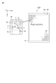
図1は、本実施形態に係る表示装置DSPの構成例を示す図である。表示装置DSPは、絶縁性の基板10の上に、画像を表示する表示領域DAと、表示領域DAの周辺の周辺領域SAとを有している。基板10は、ガラスであってもよいし、可撓性を有する樹脂フィルムであってもよい。
FIG. 1 is a diagram showing a configuration example of a display device DSP according to this embodiment. The display device DSP includes, on an
本実施形態においては、平面視における基板10の形状が長方形である。ただし、基板10の平面視における形状は長方形に限らず、正方形、円形あるいは楕円形などの他の形状であってもよい。
In this embodiment, the shape of the
表示領域DAは、第1方向Xおよび第2方向Yにマトリクス状に配列された複数の画素PXを備えている。画素PXは、複数の副画素SPを含む。一例では、画素PXは、赤色の副画素SP1、緑色の副画素SP2および青色の副画素SP3を含む。なお、画素PXは、副画素SP1,SP2,SP3とともに、あるいは副画素SP1,SP2,SP3のいずれかに代えて、白色などの他の色の副画素SPを含んでもよい。 The display area DA includes a plurality of pixels PX arranged in a matrix in a first direction X and a second direction Y. Pixel PX includes a plurality of sub-pixels SP. In one example, pixel PX includes a red subpixel SP1, a green subpixel SP2, and a blue subpixel SP3. Note that the pixel PX may include a subpixel SP of another color such as white together with the subpixels SP1, SP2, and SP3, or in place of any of the subpixels SP1, SP2, and SP3.
副画素SPは、画素回路1と、画素回路1によって駆動される表示素子20とを備えている。画素回路1は、画素スイッチ2と、駆動トランジスタ3と、キャパシタ4とを備えている。画素スイッチ2および駆動トランジスタ3は、例えば薄膜トランジスタにより構成されたスイッチング素子である。
The subpixel SP includes a
画素スイッチ2のゲート電極は、走査線GLに接続されている。画素スイッチ2のソース電極およびドレイン電極の一方は信号線SLに接続され、他方は駆動トランジスタ3のゲート電極およびキャパシタ4に接続されている。駆動トランジスタ3において、ソース電極およびドレイン電極の一方は電源線PLおよびキャパシタ4に接続され、他方は表示素子20に接続されている。
A gate electrode of the
表示素子20は、発光素子としての有機発光ダイオード(OLED)である。例えば、副画素SP1は赤色の波長域の光を放つ表示素子20を備え、副画素SP2は緑色の波長域の光を放つ表示素子20を備え、副画素SP3は青色の波長域の光を放つ表示素子20を備えている。
The
なお、画素回路1の構成は図示した例に限らない。例えば、画素回路1は、より多くの薄膜トランジスタおよびキャパシタを備えてもよい。
Note that the configuration of the
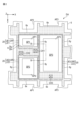
図2は、副画素SP1,SP2,SP3のレイアウトの一例を示す図である。図2の例においては、副画素SP1と副画素SP2が第2方向Yに並んでいる。さらに、副画素SP1,SP2がそれぞれ副画素SP3と第1方向Xに並んでいる。 FIG. 2 is a diagram showing an example of the layout of sub-pixels SP1, SP2, and SP3. In the example of FIG. 2, the subpixel SP1 and the subpixel SP2 are lined up in the second direction Y. Further, sub-pixels SP1 and SP2 are arranged in the first direction X with sub-pixel SP3, respectively.
副画素SP1,SP2,SP3がこのようなレイアウトである場合、表示領域DAには、副画素SP1,SP2が第2方向Yに交互に配置された列と、複数の副画素SP3が第2方向Yに繰り返し配置された列とが形成される。これらの列は、第1方向Xに交互に並ぶ。 When the subpixels SP1, SP2, and SP3 have such a layout, the display area DA includes a column in which the subpixels SP1 and SP2 are arranged alternately in the second direction Y, and a plurality of subpixels SP3 in the second direction. Y repeating rows are formed. These rows are arranged alternately in the first direction X.
なお、副画素SP1,SP2,SP3のレイアウトは図2の例に限られない。他の一例として、各画素PXにおける副画素SP1,SP2,SP3が第1方向Xに順に並んでいてもよい。 Note that the layout of the subpixels SP1, SP2, and SP3 is not limited to the example in FIG. 2. As another example, sub-pixels SP1, SP2, and SP3 in each pixel PX may be arranged in order in the first direction X.
表示領域DAには、リブ5および隔壁6が配置されている。リブ5は、副画素SP1,SP2,SP3においてそれぞれ画素開口AP1,AP2,AP3を有している。図2の例においては、画素開口AP2が画素開口AP1よりも大きく、画素開口AP3が画素開口AP2よりも大きい。
隔壁6は、隣り合う副画素SPの境界に配置され、平面視においてリブ5と重なっている。隔壁6は、第1方向Xに延びる複数の第1隔壁6xと、第2方向Yに延びる複数の第2隔壁6yとを有している。複数の第1隔壁6xは、第2方向Yに隣り合う画素開口AP1,AP2の間、および、第2方向Yに隣り合う2つの画素開口AP3の間にそれぞれ配置されている。第2隔壁6yは、第1方向Xに隣り合う画素開口AP1,AP3の間、および、第1方向Xに隣り合う画素開口AP2,AP3の間にそれぞれ配置されている。
The
図2の例においては、第1隔壁6xおよび第2隔壁6yが互いに接続されている。これにより、隔壁6は全体として画素開口AP1,AP2,AP3を囲う格子状である。隔壁6は、リブ5と同様に副画素SP1,SP2,SP3において開口を有するということもできる。
In the example of FIG. 2, the
副画素SP1は、画素開口AP1とそれぞれ重なる下電極LE1、上電極UE1および有機層OR1を備えている。副画素SP2は、画素開口AP2とそれぞれ重なる下電極LE2、上電極UE2および有機層OR2を備えている。副画素SP3は、画素開口AP3とそれぞれ重なる下電極LE3、上電極UE3および有機層OR3を備えている。図2の例においては、上電極UE1および有機層OR1の外形が一致し、上電極UE2および有機層OR2の外形が一致し、上電極UE3および有機層OR3の外形が一致している。 The sub-pixel SP1 includes a lower electrode LE1, an upper electrode UE1, and an organic layer OR1, each of which overlaps the pixel opening AP1. The sub-pixel SP2 includes a lower electrode LE2, an upper electrode UE2, and an organic layer OR2, each of which overlaps the pixel opening AP2. The subpixel SP3 includes a lower electrode LE3, an upper electrode UE3, and an organic layer OR3, each of which overlaps the pixel opening AP3. In the example of FIG. 2, the outer shapes of the upper electrode UE1 and the organic layer OR1 match, the outer shapes of the upper electrode UE2 and the organic layer OR2 match, and the outer shapes of the upper electrode UE3 and the organic layer OR3 match.
下電極LE1、上電極UE1および有機層OR1は、副画素SP1の表示素子20を構成する。下電極LE2、上電極UE2および有機層OR2は、副画素SP2の表示素子20を構成する。下電極LE3、上電極UE3および有機層OR3は、副画素SP3の表示素子20を構成する。
The lower electrode LE1, the upper electrode UE1, and the organic layer OR1 constitute the
下電極LE1は、コンタクトホールCH1を通じて副画素SP1の画素回路1(図1参照)に接続されている。下電極LE2は、コンタクトホールCH2を通じて副画素SP2の画素回路1に接続されている。下電極LE3は、コンタクトホールCH3を通じて副画素SP3の画素回路1に接続されている。
The lower electrode LE1 is connected to the pixel circuit 1 (see FIG. 1) of the subpixel SP1 through the contact hole CH1. The lower electrode LE2 is connected to the
図2の例において、コンタクトホールCH1,CH2は、第2方向Yに隣り合う画素開口AP1,AP2の間の第1隔壁6xと全体的に重なっている。コンタクトホールCH3は、第2方向Yに隣り合う2つの画素開口AP3の間の第1隔壁6xと全体的に重なっている。他の例として、コンタクトホールCH1,CH2,CH3の少なくとも一部が第1隔壁6xと重なっていなくてもよい。
In the example of FIG. 2, the contact holes CH1 and CH2 completely overlap the
図3は、図2中のIII-III線に沿う表示装置DSPの概略的な断面図である。上述の基板10の上に回路層11が配置されている。回路層11は、図1に示した画素回路1、走査線GL、信号線SLおよび電源線PLなどの各種回路や配線を含む。回路層11は、有機絶縁層12により覆われている。有機絶縁層12は、回路層11により生じる凹凸を平坦化する平坦化膜として機能する。図3の断面には表れていないが、上述のコンタクトホールCH1,CH2,CH3は有機絶縁層12に設けられている。
FIG. 3 is a schematic cross-sectional view of the display device DSP along line III-III in FIG. A
下電極LE1,LE2,LE3は、有機絶縁層12の上に配置されている。リブ5は、有機絶縁層12および下電極LE1,LE2,LE3の上に配置されている。下電極LE1,LE2,LE3の端部は、リブ5により覆われている。
The lower electrodes LE1, LE2, LE3 are arranged on the organic insulating
隔壁6は、リブ5の上に配置された導電性を有する下部61と、下部61の上に配置された上部62とを含む。上部62は、下部61よりも大きい幅を有している。これにより、図3においては上部62の両端部が下部61の側面よりも突出している。このような隔壁6の形状は、オーバーハング状ということもできる。
The
有機層OR1は、画素開口AP1を通じて下電極LE1を覆っている。上電極UE1は、有機層OR1を覆い、下電極LE1と対向している。有機層OR2は、画素開口AP2を通じて下電極LE2を覆っている。上電極UE2は、有機層OR2を覆い、下電極LE2と対向している。有機層OR3は、画素開口AP3を通じて下電極LE3を覆っている。上電極UE3は、有機層OR3を覆い、下電極LE3と対向している。 The organic layer OR1 covers the lower electrode LE1 through the pixel opening AP1. The upper electrode UE1 covers the organic layer OR1 and faces the lower electrode LE1. The organic layer OR2 covers the lower electrode LE2 through the pixel opening AP2. The upper electrode UE2 covers the organic layer OR2 and faces the lower electrode LE2. The organic layer OR3 covers the lower electrode LE3 through the pixel opening AP3. The upper electrode UE3 covers the organic layer OR3 and faces the lower electrode LE3.
図3の例においては、有機層OR1の上にキャップ層CP1が配置され、有機層OR2の上にキャップ層CP2が配置され、有機層OR3の上にキャップ層CP3が配置されている。キャップ層CP1,CP2,CP3は、それぞれ有機層OR1,OR2,OR3が発する光の光学特性を調整する。 In the example of FIG. 3, a cap layer CP1 is arranged on the organic layer OR1, a cap layer CP2 is arranged on the organic layer OR2, and a cap layer CP3 is arranged on the organic layer OR3. The cap layers CP1, CP2, and CP3 adjust the optical characteristics of the light emitted by the organic layers OR1, OR2, and OR3, respectively.
有機層OR1、上電極UE1およびキャップ層CP1の一部は、上部62の上に位置している。当該一部は、有機層OR1、上電極UE1およびキャップ層CP1の他の部分と離間している。同様に、有機層OR2、上電極UE2およびキャップ層CP2の一部は上部62の上に位置し、当該一部は有機層OR2、上電極UE2およびキャップ層CP2の他の部分と離間している。さらに、有機層OR3、上電極UE3およびキャップ層CP3の一部は上部62の上に位置し、当該一部は有機層OR3、上電極UE3およびキャップ層CP3の他の部分と離間している。
Parts of the organic layer OR1, the upper electrode UE1 and the cap layer CP1 are located above the
副画素SP1,SP2,SP3には、封止層SE1,SE2,SE3がそれぞれ配置されている。封止層SE1は、キャップ層CP1や隔壁6を連続的に覆っている。封止層SE2は、キャップ層CP2や隔壁6を連続的に覆っている。封止層SE3は、キャップ層CP3や隔壁6を連続的に覆っている。
Sealing layers SE1, SE2, and SE3 are arranged in the subpixels SP1, SP2, and SP3, respectively. The sealing layer SE1 continuously covers the cap layer CP1 and the
図3の例においては、副画素SP1,SP3の間の隔壁6上の有機層OR1、上電極UE1、キャップ層CP1および封止層SE1と、当該隔壁6上の有機層OR3、上電極UE3、キャップ層CP3および封止層SE3とが離間している。また、副画素SP2,SP3の間の隔壁6上の有機層OR2、上電極UE2、キャップ層CP2および封止層SE2と、当該隔壁6上の有機層OR3、上電極UE3、キャップ層CP3および封止層SE3とが離間している。
In the example of FIG. 3, the organic layer OR1, upper electrode UE1, cap layer CP1, and sealing layer SE1 on the
封止層SE1,SE2,SE3は、樹脂層13により覆われている。樹脂層13は、封止層14により覆われている。さらに、封止層14は、樹脂層15により覆われている。
The sealing layers SE1, SE2, SE3 are covered with a
有機絶縁層12および樹脂層13,15は、有機材料で形成されている。リブ5および封止層14,SE1,SE2,SE3は、例えばシリコン窒化物(SiNx)などの無機材料で形成されている。リブ5および封止層14,SE1,SE2,SE3は、シリコン酸化物(SiOx)、シリコン酸窒化物(SiON)または酸化アルミニウム(Al2O3)のいずれかの単層体として形成されてもよい。また、リブ5および封止層14,SE1,SE2,SE3は、シリコン窒化物層、シリコン酸化物層、シリコン酸窒化物層および酸化アルミニウム層のうちの少なくとも2つの組合せによる積層体として形成されてもよい。
The organic insulating
上電極UE1,UE2,UE3は、例えばマグネシウムと銀の合金(MgAg)などの金属材料で形成されている。下電極LE1,LE2,LE3の電位が上電極UE1,UE2,UE3の電位よりも相対的に高い場合、下電極LE1,LE2,LE3がアノードに相当し、上電極UE1,UE2,UE3がカソードに相当する。また、上電極UE1,UE2,UE3の電位が下電極LE1,LE2,LE3の電位よりも相対的に高い場合、上電極UE1,UE2,UE3がアノードに相当し、下電極LE1,LE2,LE3がカソードに相当する。 The upper electrodes UE1, UE2, and UE3 are made of a metal material such as an alloy of magnesium and silver (MgAg). When the potential of the lower electrodes LE1, LE2, LE3 is relatively higher than the potential of the upper electrodes UE1, UE2, UE3, the lower electrodes LE1, LE2, LE3 correspond to anodes, and the upper electrodes UE1, UE2, UE3 correspond to cathodes. Equivalent to. Further, when the potential of the upper electrodes UE1, UE2, UE3 is relatively higher than the potential of the lower electrodes LE1, LE2, LE3, the upper electrodes UE1, UE2, UE3 correspond to anodes, and the lower electrodes LE1, LE2, LE3 correspond to the anodes. Corresponds to the cathode.
有機層OR1,OR2,OR3は、一対の機能層と、これら機能層の間に配置された発光層とを含む。一例として、有機層OR1,OR2,OR3は、正孔注入層、正孔輸送層、電子ブロッキング層、発光層、正孔ブロッキング層、電子輸送層および電子注入層を順に積層した構造を有している。 The organic layers OR1, OR2, OR3 include a pair of functional layers and a light emitting layer disposed between these functional layers. As an example, the organic layers OR1, OR2, and OR3 have a structure in which a hole injection layer, a hole transport layer, an electron blocking layer, a light emitting layer, a hole blocking layer, an electron transport layer, and an electron injection layer are laminated in this order. There is.
キャップ層CP1,CP2,CP3は、例えば、透明な複数の薄膜の多層体によって形成されている。多層体は、複数の薄膜として、無機材料によって形成された薄膜および有機材料によって形成された薄膜を含んでもよい。また、これらの複数の薄膜は、互いに異なる屈折率を有している。多層体を構成する薄膜の材料は、上電極UE1,UE2,UE3の材料とは異なり、また、封止層SE1,SE2,SE3の材料とも異なる。なお、キャップ層CP1,CP2,CP3は省略されてもよい。 The cap layers CP1, CP2, and CP3 are formed of, for example, a multilayer body of a plurality of transparent thin films. The multilayer body may include a thin film formed of an inorganic material and a thin film formed of an organic material as the plurality of thin films. Moreover, these plurality of thin films have mutually different refractive indexes. The material of the thin film constituting the multilayer body is different from the material of the upper electrodes UE1, UE2, UE3, and also different from the material of the sealing layers SE1, SE2, SE3. Note that the cap layers CP1, CP2, and CP3 may be omitted.
隔壁6には、共通電圧が供給されている。この共通電圧は、下部61の側面に接触した上電極UE1,UE2,UE3にそれぞれ供給される。下電極LE1,LE2,LE3には、副画素SP1,SP2,SP3がそれぞれ有する画素回路1を通じて画素電圧が供給される。
A common voltage is supplied to the
下電極LE1と上電極UE1の間に電位差が形成されると、有機層OR1の発光層が赤色の波長域の光を放つ。下電極LE2と上電極UE2の間に電位差が形成されると、有機層OR2の発光層が緑色の波長域の光を放つ。下電極LE3と上電極UE3の間に電位差が形成されると、有機層OR3の発光層が青色の波長域の光を放つ。 When a potential difference is formed between the lower electrode LE1 and the upper electrode UE1, the light emitting layer of the organic layer OR1 emits light in the red wavelength range. When a potential difference is formed between the lower electrode LE2 and the upper electrode UE2, the light emitting layer of the organic layer OR2 emits light in the green wavelength range. When a potential difference is formed between the lower electrode LE3 and the upper electrode UE3, the light emitting layer of the organic layer OR3 emits light in the blue wavelength range.
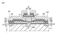
図4は、副画素SP1,SP2の境界に配置された隔壁6とその近傍を拡大した概略的な断面図である。この図においては、基板10、回路層11、樹脂層13、封止層14および樹脂層15を省略している。
FIG. 4 is an enlarged schematic cross-sectional view of the
隔壁6の下部61は、側面F1,F2を有している。隔壁6の上部62は、側面F1から突出した端部E1と、側面F2から突出した端部E2とを有している。上電極UE1,UE3は、それぞれ側面F1,F2に接触している。
The
図4の例において、下部61は、第1金属層611と、第1金属層611よりも薄い第2金属層612有している。第2金属層612は、リブ5と第1金属層611の間に位置している。また、上部62は、第1金属層611の上に配置された第1薄膜621と、第1薄膜621の上に配置された第2薄膜622とを有している。
In the example of FIG. 4, the
第1金属層611は、例えばアルミニウム(Al)によって形成されている。第1金属層611は、アルミニウム合金によって形成されてもよいし、アルミニウムとアルミニウム合金の積層構造を有してもよい。第2金属層612は、例えばモリブデン(Mo)によって形成されている。
The
第1薄膜621は、例えばチタン(Ti)によって形成されている。第1薄膜621は、シリコン酸化物などの無機材料で形成されてもよい。第2薄膜622は、例えばITO(IndiumTin Oxide)、IZO(IndiumZinc Oxide)およびIGZO(IndiumGallium Zinc Oxide)などの透明な導電性酸化物によって形成されている。なお、上部62は、チタンやシリコン酸化物などの単層構造を有してもよい。
The first
図4の例において、下電極LE1は、第1導電性酸化物層L1と、第2導電性酸化物層L2と、これら導電性酸化物層L1,L2の間の中間層L3とを有している。第1導電性酸化物層L1は中間層L3の上面を覆い、第2導電性酸化物層L2は中間層L3の下面を覆っている。 In the example of FIG. 4, the lower electrode LE1 includes a first conductive oxide layer L1, a second conductive oxide layer L2, and an intermediate layer L3 between these conductive oxide layers L1 and L2. ing. The first conductive oxide layer L1 covers the upper surface of the intermediate layer L3, and the second conductive oxide layer L2 covers the lower surface of the intermediate layer L3.
導電性酸化物層L1,L2は、例えばITOによって形成されている。すなわち、下電極LE1の上面および下面は、ITOによって形成されている。他の例として、導電性酸化物層L1,L2は、IZOまたはIGZOなどで形成されてもよい。中間層L3は、例えば銀(Ag)などの金属材料で形成されている。下電極LE2,LE3も下電極LE1と同様の構成を有している。 The conductive oxide layers L1 and L2 are made of, for example, ITO. That is, the upper and lower surfaces of the lower electrode LE1 are formed of ITO. As another example, the conductive oxide layers L1 and L2 may be formed of IZO, IGZO, or the like. The intermediate layer L3 is made of a metal material such as silver (Ag), for example. The lower electrodes LE2 and LE3 also have the same configuration as the lower electrode LE1.
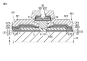
図5は、隔壁6に適用し得る構造の他の例を示す概略的な断面図である。この図の例においては、下部61が図4に示した第2金属層612を有していない。すなわち、下部61は、第1金属層611によって形成されている。第1金属層611は、リブ5の上面に接触している。
FIG. 5 is a schematic cross-sectional view showing another example of a structure that can be applied to the
図5の例においても、第1金属層611は、アルミニウムやアルミニウム合金によって形成されてもよいし、アルミニウムとアルミニウム合金の積層構造を有してもよい。
Also in the example of FIG. 5, the
続いて、周辺領域SAに適用し得る構造につき説明する。
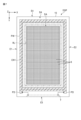
図6は、表示装置DSPの概略的な平面図である。表示装置DSPは、周辺領域SAに配置される要素として、第1ゲート駆動回路GD1、第2ゲート駆動回路GD2、セレクタ回路STおよび端子部Tを備えている。第1ゲート駆動回路GD1、第2ゲート駆動回路GD2およびセレクタ回路STは、それぞれ画素回路1に信号を供給する駆動回路の一例であり、図3に示した回路層11に含まれる。
Next, a structure applicable to the peripheral area SA will be explained.
FIG. 6 is a schematic plan view of the display device DSP. The display device DSP includes a first gate drive circuit GD1, a second gate drive circuit GD2, a selector circuit ST, and a terminal portion T as elements arranged in the peripheral area SA. The first gate drive circuit GD1, the second gate drive circuit GD2, and the selector circuit ST are examples of drive circuits that supply signals to the
第1ゲート駆動回路GD1および第2ゲート駆動回路GD2は、図1に示した走査線GLに走査信号を供給する。端子部Tには、例えばフレキシブル回路基板が接続される。セレクタ回路STは、このフレキシブル回路基板から入力される映像信号を図1に示した信号線SLに供給する。 The first gate drive circuit GD1 and the second gate drive circuit GD2 supply scanning signals to the scanning lines GL shown in FIG. For example, a flexible circuit board is connected to the terminal portion T. The selector circuit ST supplies the video signal input from this flexible circuit board to the signal line SL shown in FIG.
基板10は、第1端部E1、第2端部E2、第3端部E3および第4端部E4を有している。第1端部E1および第2端部E2は、第2方向Yと平行に延びている。第3端部E3および第4端部E4は、第1方向Xと平行に延びている。
The
図6の例においては、第1ゲート駆動回路GD1が表示領域DAと第1端部E1の間に配置され、第2ゲート駆動回路GD2が表示領域DAと第2端部E2の間に配置され、セレクタ回路STおよび端子部Tが表示領域DAと第3端部E3の間に配置されている。 In the example of FIG. 6, the first gate drive circuit GD1 is arranged between the display area DA and the first end E1, and the second gate drive circuit GD2 is arranged between the display area DA and the second end E2. , a selector circuit ST and a terminal section T are arranged between the display area DA and the third end E3.
さらに、表示装置DSPは、周辺領域SAに配置された導電層CL(ドット模様を付した部分)およびダム構造DS(斜線模様を付した部分)を備えている。図6の例においては、導電層CLが表示領域DAを囲っている。また、ダム構造DSが導電層CLを囲っている。導電層CLおよびダム構造DSは、部分的に重なっている。例えば、ダム構造DSは、図2に示した樹脂層13を堰き止める役割を担う。
Furthermore, the display device DSP includes a conductive layer CL (portion with a dot pattern) and a dam structure DS (portion with a diagonal pattern) arranged in the peripheral area SA. In the example of FIG. 6, the conductive layer CL surrounds the display area DA. Further, a dam structure DS surrounds the conductive layer CL. The conductive layer CL and the dam structure DS partially overlap. For example, the dam structure DS plays a role of damming up the
導電層CLは、表示領域DAに配置された隔壁6と接続されている。導電層CLは、第1ゲート駆動回路GD1、第2ゲート駆動回路GD2およびセレクタ回路STと平面視において重なっている。
The conductive layer CL is connected to the
なお、導電層CLは、必ずしも表示領域DAを囲う形状を有する必要はない。例えば、表示領域DAと第3端部E3の間や、表示領域DAと第4端部E4の間に導電層CLが配置されていなくてもよい。 Note that the conductive layer CL does not necessarily have to have a shape that surrounds the display area DA. For example, the conductive layer CL may not be arranged between the display area DA and the third end E3 or between the display area DA and the fourth end E4.
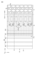
図7は、周辺領域SAに配置される他の要素を示す概略的な平面図である。周辺領域SAには、給電線PW(斜線模様を付した部分)および中継配線RL(ドット模様を付した部分)が配置されている。 FIG. 7 is a schematic plan view showing other elements arranged in the peripheral area SA. In the peripheral area SA, a power supply line PW (shaded area) and a relay wiring RL (dotted area) are arranged.
図7においては給電線PWおよび中継配線RLが表示領域DAを囲っているが、この例に限られない。給電線PWおよび中継配線RLは、部分的に重なっている。 In FIG. 7, the power supply line PW and the relay wiring RL surround the display area DA, but the present invention is not limited to this example. The power supply line PW and the relay wiring RL partially overlap.
給電線PWは、第3端部E3の近傍に位置する一対のパッドPDを有している。これらパッドPDは、端子部Tと電気的に接続されている。給電線PWには、端子部Tおよび各パッドPDを通じて共通電圧が供給される。さらに、給電線PWの共通電圧は、中継配線RLに供給される。 The power supply line PW has a pair of pads PD located near the third end E3. These pads PD are electrically connected to the terminal portion T. A common voltage is supplied to the power supply line PW through the terminal portion T and each pad PD. Furthermore, the common voltage of the power supply line PW is supplied to the relay wiring RL.
図8は、図6において鎖線枠VIIIで囲った領域の拡大図である。図9は、図8におけるIX-IX線に沿う表示装置DSPの概略的な断面図である。図8においてドット模様を付した領域が導電層CLおよび隔壁6(第1隔壁6xおよび第2隔壁6y)に相当する。導電層CLおよび隔壁6は、同じ材料で同じ製造プロセスにより一体的に形成されている。
FIG. 8 is an enlarged view of the area surrounded by a chain line frame VIII in FIG. FIG. 9 is a schematic cross-sectional view of the display device DSP along line IX-IX in FIG. In FIG. 8, the dotted regions correspond to the conductive layer CL and the partition walls 6 (the
図8および図9に示すように、ダム構造DSは、第1凸部R1、第2凸部R2、第3凸部R3および第4凸部R4を有している。第1凸部R1は表示領域DAを囲い、第2凸部R2は第1凸部R1を囲い、第3凸部R3は第2凸部R2を囲い、第4凸部R4は第3凸部R3を囲う。なお、ダム構造DSが有する凸部の数は4つに限定されず、3つ以下または5つ以上であってもよい。 As shown in FIGS. 8 and 9, the dam structure DS has a first protrusion R1, a second protrusion R2, a third protrusion R3, and a fourth protrusion R4. The first convex portion R1 surrounds the display area DA, the second convex portion R2 surrounds the first convex portion R1, the third convex portion R3 surrounds the second convex portion R2, and the fourth convex portion R4 surrounds the third convex portion Surround R3. Note that the number of protrusions that the dam structure DS has is not limited to four, and may be three or less or five or more.
図9に示すように、凸部R1,R2,R3,R4は、有機絶縁層12の端部12aと基板10の第1端部E1の間に位置している。凸部R1,R2,R3,R4は、端部12aと第2端部E2の間、端部12aと第3端部E3の間、端部12aと第4端部E4の間にも位置している。凸部R1,R2,R3,R4は、例えば有機絶縁層12と同じ材料で同じプロセスにより形成されている。
As shown in FIG. 9, the protrusions R1, R2, R3, and R4 are located between the
凸部R1,R2,R3,R4のうち隣り合う2つの間隔は、凸部R1,R2,R3,R4のそれぞれの幅よりも大きい。一例として、凸部R1,R2,R3,R4のそれぞれの幅は15~25μmであり、凸部R1,R2,R3,R4のうち隣り合う2つの間隔は25~35μmである。また、凸部R1,R2,R3,R4のそれぞれの高さは3~4μmである。 The interval between two adjacent protrusions R1, R2, R3, and R4 is larger than the width of each of the protrusions R1, R2, R3, and R4. As an example, the width of each of the protrusions R1, R2, R3, and R4 is 15 to 25 μm, and the interval between two adjacent protrusions R1, R2, R3, and R4 is 25 to 35 μm. Further, the height of each of the convex portions R1, R2, R3, and R4 is 3 to 4 μm.
図9の例において、回路層11は、絶縁層31,32,33および金属層41,42,43を備えている。絶縁層31は、基板10を覆っている。金属層41は、絶縁層31の上に配置され、絶縁層32により覆われている。金属層42は、絶縁層32の上に配置され、絶縁層33により覆われている。金属層43は、絶縁層33の上に配置され、有機絶縁層12により覆われている。
In the example of FIG. 9, the
絶縁層31,32,33は、例えばシリコン窒化物およびシリコン酸化物などの無機材料で形成されている。金属層41,42,43は、例えばモリブデン(Mo)、タングステン(W)、モリブデンタングステン合金(MoW)、アルミニウム(Al)および銅(Cu)などの金属材料の単層構造または積層構造を有している。 The insulating layers 31, 32, and 33 are made of inorganic materials such as silicon nitride and silicon oxide. The metal layers 41, 42, 43 have a single layer structure or a multilayer structure of metal materials such as molybdenum (Mo), tungsten (W), molybdenum tungsten alloy (MoW), aluminum (Al), and copper (Cu), for example. ing.
第1ゲート駆動回路GD1は、金属層41,42,43や半導体層によって形成されている。図6に示した第2ゲート駆動回路GD2およびセレクタ回路STや、図1に示した画素回路1も同様に、金属層41,42,43や半導体層によって形成されている。また、図1に示した走査線GL、信号線SLおよび電源線PLは、金属層41,42,43のいずれかによって形成されている。
The first gate drive circuit GD1 is formed of
凸部R1,R2,R3,R4は、絶縁層33の上に配置されている。リブ5は、周辺領域SAにも配置されている。図9の例においては、ダム構造DSにリブ5が配置されていない。
The convex portions R1, R2, R3, and R4 are arranged on the insulating
導電層CLは、周辺領域SAにおいてリブ5を覆っている。導電層CLは、図3乃至図5に示した隔壁6と同じく下部61および上部62を含む。導電層CLにおいても、上部62の端部が下部61の側面よりも突出している。
The conductive layer CL covers the
図8および図9に示すように、導電層CLは、ダム構造DSの一部を覆っている。導電層CLの端部CLaは、第1凸部R1と基板10の第1端部E1の間に位置している。導電層CLの端部CLaは、第1凸部R1と第2端部E2の間、第1凸部R1と第3端部E3の間、第1凸部R1と第4端部E4の間にも位置している。すなわち、端部CLaは、全周にわたり第1凸部R1と基板10の端部の間に位置している。また、図6に示すように、端部CLaは、第1ゲート駆動回路GD1と第1端部E1の間、第2ゲート駆動回路GD2と第2端部E2の間、セレクタ回路STと第3端部E3の間に位置している。
As shown in FIGS. 8 and 9, the conductive layer CL partially covers the dam structure DS. An end CLa of the conductive layer CL is located between the first convex portion R1 and the first end E1 of the
図9の例においては、導電層CLが第1凸部R1を覆っている、さらに、端部CLaが凸部R1,R2の間において絶縁層33の上に位置している。この例に限られず、端部CLaは、凸部R2,R3の間や凸部R3,R4の間に位置してもよい。
In the example of FIG. 9, the conductive layer CL covers the first convex portion R1, and further, the end portion CLa is located on the insulating
図9の例において、給電線PWは、金属層42によって形成された第1部分P1と、金属層43によって形成された第2部分P2とを有している。第2部分P2は、第1部分P1に接触している。例えば、図7に示した給電線PWのうち、パッドPDは第1部分P1によって形成され、表示領域DAを囲う部分は少なくとも第2部分P2によって形成されている。
In the example of FIG. 9, the power supply line PW has a first portion P1 formed by the metal layer 42 and a second portion P2 formed by the
中継配線RLは、大部分が有機絶縁層12の上に配置され、リブ5によって覆われている。中継配線RLは、下電極LE1,LE2,LE3と同じ材料で同じ製造プロセスにより形成されている。したがって、中継配線RLは、下電極LE1,LE2,LE3と同じく第1導電性酸化物層L1、第2導電性酸化物層L2および中間層L3を有している。
Most of the relay wiring RL is arranged on the organic insulating
中継配線RLは、第1コンタクト部CN1において給電線PWに接続され、第2コンタクト部CN2において導電層CLに接続されている。これにより、導電層CLには、中継配線RLを介して給電線PWの共通電圧が供給される。さらに、導電層CLの共通電圧は表示領域DAの隔壁6および上電極UE1,UE2,UE3に供給される。
The relay wiring RL is connected to the power supply line PW at the first contact portion CN1, and connected to the conductive layer CL at the second contact portion CN2. Thereby, the common voltage of the power supply line PW is supplied to the conductive layer CL via the relay wiring RL. Further, the common voltage of the conductive layer CL is supplied to the
第1コンタクト部CN1は、有機絶縁層12の端部12aと第1凸部R1の間に位置している。第1コンタクト部CN1においては、中継配線RLの下面が給電線PWの第2部分P2に接触している。
The first contact portion CN1 is located between the
図9の例では、第1コンタクト部CN1において、中継配線RLの上面が導電層CLの下部61に接触している。これにより、第1コンタクト部CN1においても給電線PWと導電層CLが電気的に接続される。
In the example of FIG. 9, the upper surface of the relay wiring RL is in contact with the
第1コンタクト部CN1は、例えば図7において給電線PWと中継配線RLが重なった領域に相当し、表示領域DAを囲っている。ただし、第1コンタクト部CN1は、表示領域DAの周囲の少なくとも1か所において途切れていてもよい。 The first contact portion CN1 corresponds to, for example, a region where the power supply line PW and the relay wire RL overlap in FIG. 7, and surrounds the display area DA. However, the first contact portion CN1 may be interrupted at at least one location around the display area DA.
図8および図9に示すように、第2コンタクト部CN2は、リブ5に設けられた複数のコンタクトホールCHaを有している。導電層CLの下部61は、これらコンタクトホールCHaを通じて中継配線RLの上面に接触している。
As shown in FIGS. 8 and 9, the second contact portion CN2 has a plurality of contact holes CHa provided in the
図8の例においては、複数のコンタクトホールCHaがいずれも第1方向Xに長尺に延びるとともに第2方向Yに並んでいる。コンタクトホールCHaの形状および配置はこの例に限られず、種々の態様に変形し得る。 In the example of FIG. 8, the plurality of contact holes CHa all extend in the first direction X and are lined up in the second direction Y. The shape and arrangement of contact hole CHa are not limited to this example, and may be modified in various ways.
図8に示すように、第2コンタクト部CN2は、平面視において第1コンタクト部CN1と表示領域DAの間に位置している。導電層CLの端部CLaは、平面視において第1コンタクト部CN1と基板10の第1端部E1の間に位置している。端部CLaは、第1コンタクト部CN1と第2端部E2の間、第1コンタクト部CN1と第3端部E3の間、第1コンタクト部CN1と第4端部E4の間にも位置している。
As shown in FIG. 8, the second contact portion CN2 is located between the first contact portion CN1 and the display area DA in plan view. The end CLa of the conductive layer CL is located between the first contact part CN1 and the first end E1 of the
導電層CLは、第1方向Xおよび第2方向Yに一定の間隔を空けて並んだ複数の開口APaを有している。図8の例においては、これら開口APaの一部が第2方向Yに隣り合うコンタクトホールCHaの間に位置している。開口APaは、例えば平面視においてコンタクトホールCHaよりも小さい。 The conductive layer CL has a plurality of openings APa arranged at regular intervals in the first direction X and the second direction Y. In the example of FIG. 8, some of these openings APa are located between contact holes CHa adjacent in the second direction Y. For example, the opening APa is smaller than the contact hole CHa in plan view.
導電層CLおよび隔壁6の形成に際しては、先ず下部61および上部62の基となる層が表示領域DAおよび周辺領域の全体に形成され、これらの層がエッチングにより導電層CLおよび隔壁6の形状にパターニングされる。表示領域DAにおいては各副画素SP1,SP2,SP3に対応する開口(第1隔壁6xと第2隔壁6yで囲われる領域)が多く存在する。表示領域DAと周辺領域SAとでこのような開口の密度が異なると、均一なエッチングの進行を実現できない可能性がある。これに対し、導電層CLに複数の開口APaを設けることにより、表示領域DAと周辺領域SAとでエッチングの進行を均一化することができる。
When forming the conductive layer CL and the
図9に示すように、周辺領域SAには、有機層ORs、上電極UEs、キャップ層CPsおよび封止層SEsが配置されている。図9の例においては有機層ORs、上電極UEsおよびキャップ層CPsを一つの層として示しているが、実際には上電極UEsが有機層ORsを覆い、キャップ層CPsが上電極UEsを覆っている。有機層ORs、上電極UEsおよびキャップ層CPsは、導電層CLおよびダム構造DSを覆っている。封止層SEsは、有機層ORs、上電極UEsおよびキャップ層CPsを覆っている。 As shown in FIG. 9, an organic layer ORs, an upper electrode UEs, a cap layer CPs, and a sealing layer SEs are arranged in the peripheral area SA. In the example of FIG. 9, the organic layer ORs, the upper electrode UEs, and the cap layer CPs are shown as one layer, but in reality, the upper electrode UEs covers the organic layer ORs, and the cap layer CPs covers the upper electrode UEs. There is. The organic layer ORs, the upper electrode UEs and the cap layer CPs cover the conductive layer CL and the dam structure DS. The sealing layer SEs covers the organic layer ORs, the upper electrode UEs and the cap layer CPs.
有機層ORsは、有機層OR1,OR2,OR3のいずれかと同じ材料で同じプロセスにより形成されている。上電極UEsは、上電極UE1,UE2,UE3のいずれかと同じ材料で同じプロセスにより形成されている。キャップ層CPsは、キャップ層CP1,CP2,CP3のいずれかと同じ材料で同じプロセスにより形成されている。封止層SEsは、封止層SE1,SE2,SE3のいずれかと同じ材料で同じプロセスにより形成されている。一例では、有機層ORs、上電極UEs、キャップ層CPsおよび封止層SEsは、それぞれ有機層OR3、上電極UE3、キャップ層CP3および封止層SE3と同じ材料で同じプロセスにより形成されている。 The organic layer ORs is formed of the same material and by the same process as any of the organic layers OR1, OR2, OR3. The upper electrode UEs is formed of the same material and by the same process as any of the upper electrodes UE1, UE2, UE3. The cap layer CPs is formed of the same material and by the same process as any of the cap layers CP1, CP2, and CP3. The sealing layer SEs is formed of the same material and by the same process as any of the sealing layers SE1, SE2, SE3. In one example, the organic layer ORs, the upper electrode UEs, the cap layer CPs, and the sealing layer SEs are formed of the same material and by the same process as the organic layer OR3, the upper electrode UE3, the cap layer CP3, and the sealing layer SE3, respectively.
樹脂層13は、例えばインクジェット方式により形成される。凸部R1,R2,R3,R4により生じる封止層SEsの凹凸によって、硬化前の樹脂層13の拡がりが抑制される。図9においては樹脂層13の端部が第2凸部R2の近傍に位置しているが、この例に限られない。封止層14は、樹脂層13の端部の外側において封止層SEsと接触している。樹脂層15は、封止層14を全体的に覆っている。
The
図10は、導電層CLの端部CLa近傍の概略的な断面図である。導電層CLは、下部61および上部62を有している。導電層CLの下部61および上部62の層構成は、図4および図5に示した隔壁6の層構成と同様である。
FIG. 10 is a schematic cross-sectional view of the vicinity of the end CLa of the conductive layer CL. The conductive layer CL has a
端部CLaにおいて、導電層CLの下部61は、側面F3を有している。導電層CLの上部62は、側面F3よりも突出している。すなわち、端部CLaにおける導電層CLの形状は、隔壁6と同じくオーバーハング状である。
At the end CLa, the
このような形状の導電層CLの上に有機層ORs、上電極UEsおよびキャップ層CPsを形成すると、図10に示すように、端部CLaにおいてこれら有機層ORs、上電極UEsおよびキャップ層CPsが分断される。 When the organic layer ORs, upper electrode UEs, and cap layer CPs are formed on the conductive layer CL having such a shape, as shown in FIG. be divided.
封止層SEsは、導電層CLの上下にそれぞれ位置する有機層ORs、上電極UEsおよびキャップ層CPsを覆うとともに、下部61の側面F3も覆っている。
The sealing layer SEs covers the organic layer ORs, the upper electrode UEs, and the cap layer CPs located above and below the conductive layer CL, and also covers the side surface F3 of the
なお、図8乃至図10においては表示領域DAと第1端部E1の間の構造に着目したが、表示領域DAと第2端部E2の間、表示領域DAと第3端部E3の間、および、表示領域DAと第4端部E4の間にも同様の構造を適用できる。好ましくは、有機層ORs、上電極UEsおよびキャップ層CPsは、端部CLaの全周にわたり分断されている。 In addition, in FIGS. 8 to 10, attention is paid to the structure between the display area DA and the first end E1, but between the display area DA and the second end E2, and between the display area DA and the third end E3. , and a similar structure can be applied between the display area DA and the fourth end E4. Preferably, the organic layer ORs, the upper electrode UEs, and the cap layer CPs are separated over the entire circumference of the end CLa.
以上の本実施形態に係る表示装置DSPにおいては、表示領域DAに配置された隔壁6が周辺領域SAに配置された導電層CLと接続されている。さらに、隔壁6が副画素SP1,SP2,SP3の上電極UE1,UE2,UE3に接続され、導電層CLが給電線PWに接続されている。このような構造においては、給電線PWの共通電圧を、導電層CLおよび隔壁6を介して上電極UE1,UE2,UE3に供給することができる。
In the display device DSP according to the present embodiment described above, the
図9の例のように、周辺領域SAに有機層ORs、上電極UEsおよびキャップ層CPsが配置されている場合、これらの層を通じて表示装置DSP内部に水分が浸入する可能性がある。この水分がゲート駆動回路GD1,GD2、セレクタ回路ST、給電線PW、画素回路1および表示素子20などに到達すると、表示装置DSPの動作不良が生じ得る。
As in the example of FIG. 9, when the organic layer ORs, the upper electrode UEs, and the cap layer CPs are arranged in the peripheral area SA, there is a possibility that moisture may infiltrate into the display device DSP through these layers. If this moisture reaches the gate drive circuits GD1, GD2, selector circuit ST, power supply line PW,
これに対し、本実施形態に係る表示装置DSPにおいては、導電層CLの端部CLaが、ダム構造DSの第1凸部R1と基板10の端部E1,E2,E3,E4の間に位置している。これにより、図10に示したように有機層ORs、上電極UEsおよびキャップ層CPsが分断され、これらの層を通じた表示装置DSP内部への水分浸入を抑制できる。結果として、表示装置DSPの水分への耐性が向上する。図9の例のように端部CLaがコンタクト部CN1,CN2よりも外側に位置していれば、これらコンタクト部CN1,CN2を通じた水分の浸入が抑制されるため一層好適である。
In contrast, in the display device DSP according to the present embodiment, the end CLa of the conductive layer CL is located between the first convex portion R1 of the dam structure DS and the ends E1, E2, E3, and E4 of the
ダム構造DSの凸部R1,R2,R3,R4の上面は曲面となり得るため、仮に導電層CLの端部CLaがダム構造DSの凸部R1,R2,R3,R4の上に位置すると、端部CLaが良好なオーバーハング状に形成されない可能性がある。 Since the upper surface of the convex portions R1, R2, R3, R4 of the dam structure DS can be a curved surface, if the end CLa of the conductive layer CL is located on the convex portions R1, R2, R3, R4 of the dam structure DS, the edge There is a possibility that the portion CLa is not formed in a good overhang shape.
これに対し、図9の例のように端部CLaが凸部R1,R2の間に位置していれば、端部CLaを良好なオーバーハング状に形成することができる。端部CLaが凸部R2,R3の間や凸部R3,R4の間に位置する場合でも同様の効果を得ることができる。 On the other hand, if the end portion CLa is located between the convex portions R1 and R2 as in the example of FIG. 9, the end portion CLa can be formed into a good overhang shape. Similar effects can be obtained even when the end CLa is located between the protrusions R2 and R3 or between the protrusions R3 and R4.
以上、本発明の実施形態として説明した表示装置を基にして、当業者が適宜設計変更して実施し得る全ての表示装置も、本発明の要旨を包含する限り本発明の範囲に属する。 All display devices that can be implemented by appropriately modifying the design by those skilled in the art based on the display device described as an embodiment of the present invention as described above also belong to the scope of the present invention as long as they include the gist of the present invention.
本発明の思想の範疇において、当業者であれば、各種の変形例に想到し得るものであり、それら変形例についても本発明の範囲に属するものと解される。例えば、上述の各実施形態に対して、当業者が適宜、構成要素の追加、削除、もしくは設計変更を行ったもの、または、工程の追加、省略もしくは条件変更を行ったものも、本発明の要旨を備えている限り、本発明の範囲に含まれる。 Those skilled in the art will be able to come up with various modifications within the scope of the present invention, and it is understood that these modifications also fall within the scope of the present invention. For example, a person skilled in the art may appropriately add, delete, or change the design of each of the above-described embodiments, or add, omit, or change the conditions of a process. As long as it has the gist, it is within the scope of the present invention.
また、上述の各実施形態において述べた態様によりもたらされる他の作用効果について、本明細書の記載から明らかなもの、または当業者において適宜想到し得るものについては、当然に本発明によりもたらされるものと解される。 Furthermore, other effects brought about by the aspects described in each of the above-mentioned embodiments that are obvious from the description of this specification or that can be appropriately conceived by those skilled in the art are naturally brought about by the present invention. It is understood that
DSP…表示装置、DA…表示領域、SA…周辺領域、PX…画素、SP1,SP2,SP3…副画素、LE1,LE2,LE3…下電極、UE1,UE2,UE3,UEs…上電極、OR1,OR2,OR3,ORs…有機層、CP1,CP2,CP3,CPs…キャップ層、SE1,SE2,SE3,SEs…封止層、CL…導電層、PW…給電線、RL…中継配線、DS…ダム構造、R1,R2,R3,R4…凸部、CN1…第1コンタクト部、CN2…第2コンタクト部、APa…開口、CHa…コンタクトホール、1…画素回路、5…リブ、6…隔壁、10…基板、12…有機絶縁層、61…隔壁の下部、62…隔壁の上部。 DSP...display device, DA...display area, SA...peripheral area, PX...pixel, SP1, SP2, SP3...subpixel, LE1, LE2, LE3...lower electrode, UE1, UE2, UE3, UEs...upper electrode, OR1, OR2, OR3, ORs...organic layer, CP1, CP2, CP3, CPs...cap layer, SE1, SE2, SE3, SEs...sealing layer, CL...conductive layer, PW...power supply line, RL...relay wiring, DS...dam Structure, R1, R2, R3, R4... Convex portion, CN1... First contact portion, CN2... Second contact portion, APa... Opening, CHa... Contact hole, 1... Pixel circuit, 5... Rib, 6... Partition wall, 10 ... Substrate, 12... Organic insulating layer, 61... Lower part of partition, 62... Upper part of partition.
Claims (13)
前記基板の上方に配置された絶縁層と、
画素を含む表示領域において前記絶縁層の上方に配置された下電極と、
前記下電極と重なる開口を有するリブと、
前記表示領域において前記リブの上方に配置された隔壁と、
前記下電極に対向し、前記隔壁に接続された上電極と、
前記下電極と前記上電極の間に配置され、前記下電極と前記上電極の電位差に応じて発光する有機層と、
前記基板の端部と前記表示領域の間の周辺領域に配置された少なくとも1つの凸部を含むダム構造と、
前記周辺領域に配置され、前記ダム構造の少なくとも一部を覆うとともに前記隔壁に接続された導電層と、
を備え、
前記隔壁および前記導電層は、導電性を有する下部と、前記下部の側面から突出した上部と、を有し、
前記導電層の端部は、平面視において前記凸部と前記基板の端部の間に位置している、
表示装置。 A substrate and
an insulating layer disposed above the substrate;
a lower electrode disposed above the insulating layer in a display area including pixels;
a rib having an opening that overlaps with the lower electrode;
a partition wall disposed above the rib in the display area;
an upper electrode facing the lower electrode and connected to the partition wall;
an organic layer that is disposed between the lower electrode and the upper electrode and emits light according to a potential difference between the lower electrode and the upper electrode;
a dam structure including at least one convex portion disposed in a peripheral area between an end of the substrate and the display area;
a conductive layer disposed in the peripheral region, covering at least a portion of the dam structure and connected to the partition;
Equipped with
The partition wall and the conductive layer have a lower part having conductivity and an upper part protruding from a side surface of the lower part,
The end of the conductive layer is located between the convex part and the end of the substrate in plan view.
Display device.
前記導電層の端部により前記有機層が分断されている、
請求項1に記載の表示装置。 the organic layer is also arranged in the peripheral region,
the organic layer is separated by an end of the conductive layer;
The display device according to claim 1.
前記導電層の端部は、全周にわたり前記凸部と前記基板の端部の間に位置している、
請求項1または2に記載の表示装置。 the conductive layer and the convex portion surround the display area;
The end of the conductive layer is located between the convex part and the end of the substrate over the entire circumference,
The display device according to claim 1 or 2.
請求項1乃至3のうちいずれか1項に記載の表示装置。 The convex portion is formed of the same material as the insulating layer,
A display device according to any one of claims 1 to 3.
前記導電層の端部は、平面視において前記第1凸部と前記第2凸部の間に位置している、
請求項1乃至4のうちいずれか1項に記載の表示装置。 The dam structure includes a first convex portion surrounding the display area and a second convex portion surrounding the first convex portion,
The end portion of the conductive layer is located between the first convex portion and the second convex portion in plan view.
A display device according to any one of claims 1 to 4.
前記周辺領域に配置され、前記画素回路に信号を供給する駆動回路と、をさらに備え、
前記導電層の端部は、平面視において前記駆動回路と前記基板の端部の間に位置している、
請求項1乃至5のうちいずれか1項に記載の表示装置。 a pixel circuit arranged in the display area and supplying voltage to the lower electrode;
further comprising a drive circuit disposed in the peripheral area and supplying a signal to the pixel circuit,
The end of the conductive layer is located between the drive circuit and the end of the substrate in plan view.
A display device according to any one of claims 1 to 5.
前記周辺領域に位置する第1コンタクト部において前記給電線に接続され、前記周辺領域に位置する第2コンタクト部において前記導電層に接続された中継配線と、をさらに備える、
請求項1乃至6のうちいずれか1項に記載の表示装置。 a power supply line arranged in the peripheral area;
Further comprising: a relay wiring connected to the power supply line at a first contact portion located in the peripheral region and connected to the conductive layer at a second contact portion located in the peripheral region;
A display device according to any one of claims 1 to 6.
請求項7に記載の表示装置。 In the first contact portion, a lower surface of the relay wire is in contact with the power supply line, and an upper surface of the relay wire is in contact with the conductive layer.
The display device according to claim 7.
前記第2コンタクト部は、前記リブに設けられた複数のコンタクトホールを含み、
前記導電層は、前記複数のコンタクトホールを通じて前記中継配線に接触している、
請求項7または8に記載の表示装置。 The relay wiring is covered by the rib,
The second contact portion includes a plurality of contact holes provided in the rib,
the conductive layer is in contact with the relay wiring through the plurality of contact holes;
The display device according to claim 7 or 8.
請求項9に記載の表示装置。 The plurality of contact holes are elongated in a first direction and are lined up in a second direction intersecting the first direction.
The display device according to claim 9.
請求項9または10に記載の表示装置。 The conductive layer has a plurality of openings smaller than each of the plurality of contact holes.
The display device according to claim 9 or 10.
請求項7乃至11のうちいずれか1項に記載の表示装置。 The end of the conductive layer is located between the first contact part and the end of the substrate in plan view.
The display device according to any one of claims 7 to 11.
請求項7乃至11のうちいずれか1項に記載の表示装置。 The second contact portion is located between the first contact portion and the display area in plan view.
The display device according to any one of claims 7 to 11.
Priority Applications (5)
| Application Number | Priority Date | Filing Date | Title |
|---|---|---|---|
| JP2022042743A JP2023136830A (en) | 2022-03-17 | 2022-03-17 | display device |
| CN202310227374.6A CN116782684A (en) | 2022-03-17 | 2023-03-10 | display device |
| KR1020230033011A KR102905751B1 (en) | 2022-03-17 | 2023-03-14 | Display device |
| DE102023202340.7A DE102023202340A1 (en) | 2022-03-17 | 2023-03-15 | Display device |
| US18/184,699 US12568748B2 (en) | 2022-03-17 | 2023-03-16 | Display device |
Applications Claiming Priority (1)
| Application Number | Priority Date | Filing Date | Title |
|---|---|---|---|
| JP2022042743A JP2023136830A (en) | 2022-03-17 | 2022-03-17 | display device |
Publications (1)
| Publication Number | Publication Date |
|---|---|
| JP2023136830A true JP2023136830A (en) | 2023-09-29 |
Family
ID=87849546
Family Applications (1)
| Application Number | Title | Priority Date | Filing Date |
|---|---|---|---|
| JP2022042743A Pending JP2023136830A (en) | 2022-03-17 | 2022-03-17 | display device |
Country Status (5)
| Country | Link |
|---|---|
| US (1) | US12568748B2 (en) |
| JP (1) | JP2023136830A (en) |
| KR (1) | KR102905751B1 (en) |
| CN (1) | CN116782684A (en) |
| DE (1) | DE102023202340A1 (en) |
Families Citing this family (2)
| Publication number | Priority date | Publication date | Assignee | Title |
|---|---|---|---|---|
| KR20240055217A (en) * | 2022-10-19 | 2024-04-29 | 삼성디스플레이 주식회사 | Display panel |
| KR20250045506A (en) * | 2023-09-25 | 2025-04-02 | 삼성디스플레이 주식회사 | Display device |
Citations (12)
| Publication number | Priority date | Publication date | Assignee | Title |
|---|---|---|---|---|
| JP2000331784A (en) * | 1999-05-24 | 2000-11-30 | Tohoku Pioneer Corp | Organic EL display panel and manufacturing method thereof |
| US20060108917A1 (en) * | 2004-10-08 | 2006-05-25 | Chi Mei Optoelectronics Corp. | Organic electroluminescent device and fabricating method thereof |
| JP2007147814A (en) * | 2005-11-25 | 2007-06-14 | Seiko Epson Corp | LIGHT EMITTING DEVICE, ITS MANUFACTURING METHOD, AND ELECTRONIC DEVICE |
| JP2008135325A (en) * | 2006-11-29 | 2008-06-12 | Hitachi Displays Ltd | Organic EL display device and manufacturing method thereof |
| JP4637390B2 (en) * | 2000-03-27 | 2011-02-23 | 株式会社半導体エネルギー研究所 | Method for manufacturing light emitting device |
| JP5008606B2 (en) * | 2007-07-03 | 2012-08-22 | キヤノン株式会社 | Organic EL display device and manufacturing method thereof |
| JP2012182121A (en) * | 2011-02-10 | 2012-09-20 | Semiconductor Energy Lab Co Ltd | Light-emitting device, manufacturing method of the same, illuminating device and display device |
| JP5728068B2 (en) * | 2008-07-21 | 2015-06-03 | 株式会社半導体エネルギー研究所 | Deposition substrate |
| JP2018107033A (en) * | 2016-12-27 | 2018-07-05 | Lumiotec株式会社 | Organic electroluminescent element, lighting system, and display device |
| CN111033782A (en) * | 2017-08-09 | 2020-04-17 | 夏普株式会社 | Display device, method for manufacturing display device, and device for manufacturing display device |
| WO2020202247A1 (en) * | 2019-03-29 | 2020-10-08 | シャープ株式会社 | Display device |
| WO2021161465A1 (en) * | 2020-02-13 | 2021-08-19 | シャープ株式会社 | Display device |
Family Cites Families (16)
| Publication number | Priority date | Publication date | Assignee | Title |
|---|---|---|---|---|
| JP3188678B2 (en) | 1998-12-25 | 2001-07-16 | ティーディーケイ株式会社 | Organic EL display device and manufacturing method thereof |
| JP4089544B2 (en) | 2002-12-11 | 2008-05-28 | ソニー株式会社 | Display device and manufacturing method of display device |
| KR100738224B1 (en) * | 2006-03-31 | 2007-07-12 | 엘지전자 주식회사 | Electroluminescent element |
| US7834543B2 (en) | 2007-07-03 | 2010-11-16 | Canon Kabushiki Kaisha | Organic EL display apparatus and method of manufacturing the same |
| JP2010118191A (en) | 2008-11-11 | 2010-05-27 | Sharp Corp | Organic electroluminescent display device and its manufacturing method |
| US9172036B2 (en) * | 2013-11-22 | 2015-10-27 | Taiwan Semiconductor Manufacturing Co., Ltd. | Top electrode blocking layer for RRAM device |
| KR102456183B1 (en) | 2015-04-23 | 2022-10-18 | 엘지디스플레이 주식회사 | Organic light emitting display device and fabricating method thereof |
| WO2018179308A1 (en) | 2017-03-31 | 2018-10-04 | シャープ株式会社 | Display device and production method therefor |
| KR102360094B1 (en) | 2017-09-15 | 2022-02-09 | 삼성디스플레이 주식회사 | Display device |
| KR102787722B1 (en) * | 2019-06-25 | 2025-03-26 | 엘지디스플레이 주식회사 | Eletroluminescence display device |
| WO2021036411A1 (en) * | 2019-08-28 | 2021-03-04 | 云谷(固安)科技有限公司 | Display panel, display device, and manufacturing method of display panel |
| CN110890406B (en) | 2019-11-28 | 2022-07-12 | 京东方科技集团股份有限公司 | Organic light-emitting display back plate, manufacturing method thereof and display device |
| KR102909039B1 (en) | 2020-07-06 | 2026-01-07 | 삼성디스플레이 주식회사 | Display panel and mask sheet for manufacturing the same |
| KR102870804B1 (en) * | 2020-07-08 | 2025-10-14 | 삼성디스플레이 주식회사 | Display Apparatus and Method for manufacturing the same |
| JP7060659B2 (en) | 2020-09-03 | 2022-04-26 | 本田技研工業株式会社 | Body front structure |
| JP2023136831A (en) | 2022-03-17 | 2023-09-29 | 株式会社ジャパンディスプレイ | Display divice |
-
2022
- 2022-03-17 JP JP2022042743A patent/JP2023136830A/en active Pending
-
2023
- 2023-03-10 CN CN202310227374.6A patent/CN116782684A/en active Pending
- 2023-03-14 KR KR1020230033011A patent/KR102905751B1/en active Active
- 2023-03-15 DE DE102023202340.7A patent/DE102023202340A1/en active Pending
- 2023-03-16 US US18/184,699 patent/US12568748B2/en active Active
Patent Citations (12)
| Publication number | Priority date | Publication date | Assignee | Title |
|---|---|---|---|---|
| JP2000331784A (en) * | 1999-05-24 | 2000-11-30 | Tohoku Pioneer Corp | Organic EL display panel and manufacturing method thereof |
| JP4637390B2 (en) * | 2000-03-27 | 2011-02-23 | 株式会社半導体エネルギー研究所 | Method for manufacturing light emitting device |
| US20060108917A1 (en) * | 2004-10-08 | 2006-05-25 | Chi Mei Optoelectronics Corp. | Organic electroluminescent device and fabricating method thereof |
| JP2007147814A (en) * | 2005-11-25 | 2007-06-14 | Seiko Epson Corp | LIGHT EMITTING DEVICE, ITS MANUFACTURING METHOD, AND ELECTRONIC DEVICE |
| JP2008135325A (en) * | 2006-11-29 | 2008-06-12 | Hitachi Displays Ltd | Organic EL display device and manufacturing method thereof |
| JP5008606B2 (en) * | 2007-07-03 | 2012-08-22 | キヤノン株式会社 | Organic EL display device and manufacturing method thereof |
| JP5728068B2 (en) * | 2008-07-21 | 2015-06-03 | 株式会社半導体エネルギー研究所 | Deposition substrate |
| JP2012182121A (en) * | 2011-02-10 | 2012-09-20 | Semiconductor Energy Lab Co Ltd | Light-emitting device, manufacturing method of the same, illuminating device and display device |
| JP2018107033A (en) * | 2016-12-27 | 2018-07-05 | Lumiotec株式会社 | Organic electroluminescent element, lighting system, and display device |
| CN111033782A (en) * | 2017-08-09 | 2020-04-17 | 夏普株式会社 | Display device, method for manufacturing display device, and device for manufacturing display device |
| WO2020202247A1 (en) * | 2019-03-29 | 2020-10-08 | シャープ株式会社 | Display device |
| WO2021161465A1 (en) * | 2020-02-13 | 2021-08-19 | シャープ株式会社 | Display device |
Also Published As
| Publication number | Publication date |
|---|---|
| KR20230136048A (en) | 2023-09-26 |
| KR102905751B1 (en) | 2025-12-31 |
| US12568748B2 (en) | 2026-03-03 |
| US20230301159A1 (en) | 2023-09-21 |
| CN116782684A (en) | 2023-09-19 |
| DE102023202340A1 (en) | 2023-09-21 |
Similar Documents
| Publication | Publication Date | Title |
|---|---|---|
| JP2023136831A (en) | Display divice | |
| JP7767139B2 (en) | display device | |
| JP2023125466A (en) | Display device manufacturing method | |
| JP7835428B2 (en) | display device | |
| JP2023120847A (en) | Display device | |
| KR102905751B1 (en) | Display device | |
| US20240114751A1 (en) | Display device | |
| US20240298503A1 (en) | Display device | |
| JP2023106165A (en) | Display device | |
| CN116406199A (en) | display device | |
| JP2023160399A (en) | Display device and its manufacturing method | |
| US20240040905A1 (en) | Display device and manufacturing method thereof | |
| US20240040901A1 (en) | Display device and manufacturing method thereof | |
| JP2024036917A (en) | display device | |
| JP2024040805A (en) | display device | |
| JP2024021305A (en) | display device | |
| JP2024063386A (en) | Display device | |
| CN119486505A (en) | Display device | |
| CN118785789A (en) | Display device |
Legal Events
| Date | Code | Title | Description |
|---|---|---|---|
| A621 | Written request for application examination |
Free format text: JAPANESE INTERMEDIATE CODE: A621 Effective date: 20250213 |
|
| A711 | Notification of change in applicant |
Free format text: JAPANESE INTERMEDIATE CODE: A711 Effective date: 20250626 |
|
| A977 | Report on retrieval |
Free format text: JAPANESE INTERMEDIATE CODE: A971007 Effective date: 20260218 |
|
| A131 | Notification of reasons for refusal |
Free format text: JAPANESE INTERMEDIATE CODE: A131 Effective date: 20260224 |
|
| A521 | Request for written amendment filed |
Free format text: JAPANESE INTERMEDIATE CODE: A523 Effective date: 20260306 |