JP2024123726A - Magnetic head and magnetic recording device - Google Patents
Magnetic head and magnetic recording device Download PDFInfo
- Publication number
- JP2024123726A JP2024123726A JP2023031362A JP2023031362A JP2024123726A JP 2024123726 A JP2024123726 A JP 2024123726A JP 2023031362 A JP2023031362 A JP 2023031362A JP 2023031362 A JP2023031362 A JP 2023031362A JP 2024123726 A JP2024123726 A JP 2024123726A
- Authority
- JP
- Japan
- Prior art keywords
- magnetic
- voltage
- layer
- magnetic layer
- magnetic pole
- Prior art date
- Legal status (The legal status is an assumption and is not a legal conclusion. Google has not performed a legal analysis and makes no representation as to the accuracy of the status listed.)
- Pending
Links
Images









Classifications
-
- G—PHYSICS
- G11—INFORMATION STORAGE
- G11B—INFORMATION STORAGE BASED ON RELATIVE MOVEMENT BETWEEN RECORD CARRIER AND TRANSDUCER
- G11B5/00—Recording by magnetisation or demagnetisation of a record carrier; Reproducing by magnetic means; Record carriers therefor
- G11B5/127—Structure or manufacture of heads, e.g. inductive
- G11B5/31—Structure or manufacture of heads, e.g. inductive using thin films
- G11B5/3109—Details
- G11B5/313—Disposition of layers
- G11B5/3143—Disposition of layers including additional layers for improving the electromagnetic transducing properties of the basic structure, e.g. for flux coupling, guiding or shielding
- G11B5/3146—Disposition of layers including additional layers for improving the electromagnetic transducing properties of the basic structure, e.g. for flux coupling, guiding or shielding magnetic layers
-
- G—PHYSICS
- G11—INFORMATION STORAGE
- G11B—INFORMATION STORAGE BASED ON RELATIVE MOVEMENT BETWEEN RECORD CARRIER AND TRANSDUCER
- G11B5/00—Recording by magnetisation or demagnetisation of a record carrier; Reproducing by magnetic means; Record carriers therefor
- G11B5/127—Structure or manufacture of heads, e.g. inductive
- G11B5/187—Structure or manufacture of the surface of the head in physical contact with, or immediately adjacent to the recording medium; Pole pieces; Gap features
- G11B5/23—Gap features
- G11B5/235—Selection of material for gap filler
-
- G—PHYSICS
- G11—INFORMATION STORAGE
- G11B—INFORMATION STORAGE BASED ON RELATIVE MOVEMENT BETWEEN RECORD CARRIER AND TRANSDUCER
- G11B5/00—Recording by magnetisation or demagnetisation of a record carrier; Reproducing by magnetic means; Record carriers therefor
- G11B5/127—Structure or manufacture of heads, e.g. inductive
- G11B5/31—Structure or manufacture of heads, e.g. inductive using thin films
- G11B5/3109—Details
- G11B5/313—Disposition of layers
- G11B5/3133—Disposition of layers including layers not usually being a part of the electromagnetic transducer structure and providing additional features, e.g. for improving heat radiation, reduction of power dissipation, adaptations for measurement or indication of gap depth or other properties of the structure
-
- G—PHYSICS
- G11—INFORMATION STORAGE
- G11B—INFORMATION STORAGE BASED ON RELATIVE MOVEMENT BETWEEN RECORD CARRIER AND TRANSDUCER
- G11B5/00—Recording by magnetisation or demagnetisation of a record carrier; Reproducing by magnetic means; Record carriers therefor
- G11B5/127—Structure or manufacture of heads, e.g. inductive
- G11B5/31—Structure or manufacture of heads, e.g. inductive using thin films
- G11B5/3109—Details
- G11B5/313—Disposition of layers
- G11B5/3133—Disposition of layers including layers not usually being a part of the electromagnetic transducer structure and providing additional features, e.g. for improving heat radiation, reduction of power dissipation, adaptations for measurement or indication of gap depth or other properties of the structure
- G11B5/314—Disposition of layers including layers not usually being a part of the electromagnetic transducer structure and providing additional features, e.g. for improving heat radiation, reduction of power dissipation, adaptations for measurement or indication of gap depth or other properties of the structure where the layers are extra layers normally not provided in the transducing structure, e.g. optical layers
-
- G—PHYSICS
- G11—INFORMATION STORAGE
- G11B—INFORMATION STORAGE BASED ON RELATIVE MOVEMENT BETWEEN RECORD CARRIER AND TRANSDUCER
- G11B5/00—Recording by magnetisation or demagnetisation of a record carrier; Reproducing by magnetic means; Record carriers therefor
- G11B5/127—Structure or manufacture of heads, e.g. inductive
- G11B5/31—Structure or manufacture of heads, e.g. inductive using thin films
- G11B5/3109—Details
- G11B5/313—Disposition of layers
- G11B5/3143—Disposition of layers including additional layers for improving the electromagnetic transducing properties of the basic structure, e.g. for flux coupling, guiding or shielding
- G11B5/3146—Disposition of layers including additional layers for improving the electromagnetic transducing properties of the basic structure, e.g. for flux coupling, guiding or shielding magnetic layers
- G11B5/315—Shield layers on both sides of the main pole, e.g. in perpendicular magnetic heads
-
- G—PHYSICS
- G11—INFORMATION STORAGE
- G11B—INFORMATION STORAGE BASED ON RELATIVE MOVEMENT BETWEEN RECORD CARRIER AND TRANSDUCER
- G11B5/00—Recording by magnetisation or demagnetisation of a record carrier; Reproducing by magnetic means; Record carriers therefor
- G11B2005/0002—Special dispositions or recording techniques
- G11B2005/0005—Arrangements, methods or circuits
-
- G—PHYSICS
- G11—INFORMATION STORAGE
- G11B—INFORMATION STORAGE BASED ON RELATIVE MOVEMENT BETWEEN RECORD CARRIER AND TRANSDUCER
- G11B5/00—Recording by magnetisation or demagnetisation of a record carrier; Reproducing by magnetic means; Record carriers therefor
- G11B2005/0002—Special dispositions or recording techniques
- G11B2005/0005—Arrangements, methods or circuits
- G11B2005/0024—Microwave assisted recording
-
- G—PHYSICS
- G11—INFORMATION STORAGE
- G11B—INFORMATION STORAGE BASED ON RELATIVE MOVEMENT BETWEEN RECORD CARRIER AND TRANSDUCER
- G11B5/00—Recording by magnetisation or demagnetisation of a record carrier; Reproducing by magnetic means; Record carriers therefor
- G11B5/02—Recording, reproducing, or erasing methods; Read, write or erase circuits therefor
- G11B5/027—Analogue recording
-
- G—PHYSICS
- G11—INFORMATION STORAGE
- G11B—INFORMATION STORAGE BASED ON RELATIVE MOVEMENT BETWEEN RECORD CARRIER AND TRANSDUCER
- G11B5/00—Recording by magnetisation or demagnetisation of a record carrier; Reproducing by magnetic means; Record carriers therefor
- G11B5/127—Structure or manufacture of heads, e.g. inductive
- G11B5/1278—Structure or manufacture of heads, e.g. inductive specially adapted for magnetisations perpendicular to the surface of the record carrier
Landscapes
- Engineering & Computer Science (AREA)
- Manufacturing & Machinery (AREA)
- Physics & Mathematics (AREA)
- Electromagnetism (AREA)
- Magnetic Heads (AREA)
- Signal Processing For Digital Recording And Reproducing (AREA)
Abstract
Description
本発明の実施形態は、磁気ヘッド及び磁気記録装置に関する。 Embodiments of the present invention relate to a magnetic head and a magnetic recording device.
磁気ヘッドを用いて、HDD(Hard Disk Drive)などの磁気記録媒体に情報が記録される。磁気記録装置において、記録密度の向上が望まれる。 Information is recorded on magnetic recording media such as HDDs (Hard Disk Drives) using magnetic heads. In magnetic recording devices, it is desirable to improve the recording density.
本発明の実施形態は、記録密度の向上が可能な磁気ヘッド及び磁気記録装置を提供する。 Embodiments of the present invention provide a magnetic head and a magnetic recording device that can improve recording density.
実施形態によれば、磁気ヘッドは、第1磁極と、第2磁極と、前記第1磁極と前記第2磁極との間に設けられた磁気素子と、を含む。前記磁気素子は、第1磁性層と、前記第1磁性層と前記第2磁極との間に設けられた第2磁性層と、前記第2磁性層と前記第2磁極との間に設けられた第3磁性層と、前記第3磁性層と前記第2磁極との間に設けられた第4磁性層と、前記第4磁性層と前記第2磁極との間に設けられた第5磁性層と、前記第1磁極と前記第1磁性層との間に設けられた第1非磁性層と、前記第1磁性層と前記第2磁性層との間に設けられた第2非磁性層と、前記第2磁性層と前記第3磁性層との間に設けられた第3非磁性層と、前記第3磁性層と前記第4磁性層との間に設けられた第4非磁性層と、前記第4磁性層と前記第5磁性層との間に設けられた第5非磁性層と、前記第5磁性層と前記第2磁極との間に設けられた第6非磁性層と、を含む。前記第6非磁性層は、Ru、Ir、Ta、Rh、Pd、Pt及びWよりなる群から選択された少なくとも1つを含む。 According to the embodiment, the magnetic head includes a first magnetic pole, a second magnetic pole, and a magnetic element provided between the first magnetic pole and the second magnetic pole. The magnetic element includes a first magnetic layer, a second magnetic layer provided between the first magnetic layer and the second magnetic pole, a third magnetic layer provided between the second magnetic layer and the second magnetic pole, a fourth magnetic layer provided between the third magnetic layer and the second magnetic pole, a fifth magnetic layer provided between the fourth magnetic layer and the second magnetic pole, a first non-magnetic layer provided between the first magnetic pole and the first magnetic layer, a second non-magnetic layer provided between the first magnetic layer and the second magnetic layer, a third non-magnetic layer provided between the second magnetic layer and the third magnetic layer, a fourth non-magnetic layer provided between the third magnetic layer and the fourth magnetic layer, a fifth non-magnetic layer provided between the fourth magnetic layer and the fifth magnetic layer, and a sixth non-magnetic layer provided between the fifth magnetic layer and the second magnetic pole. The sixth nonmagnetic layer contains at least one selected from the group consisting of Ru, Ir, Ta, Rh, Pd, Pt, and W.
以下に、本発明の実施形態について図面を参照しつつ説明する。
図面は模式的または概念的なものであり、各部分の厚さと幅との関係、部分間の大きさの比率などは、必ずしも現実のものと同一とは限らない。同じ部分を表す場合であっても、図面により互いの寸法や比率が異なって表される場合もある。
本願明細書と各図において、既出の図に関して前述したものと同様の要素には同一の符号を付して詳細な説明は適宜省略する。
Hereinafter, an embodiment of the present invention will be described with reference to the drawings.
The drawings are schematic or conceptual, and the relationship between the thickness and width of each part, the size ratio between parts, etc. are not necessarily the same as those in reality. Even when the same part is shown, the dimensions and ratios of each part may be different depending on the drawing.
In this specification and each drawing, elements similar to those described above with reference to the previous drawings are given the same reference numerals and detailed descriptions thereof will be omitted as appropriate.
(第1実施形態)
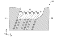
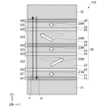
図1は、第1実施形態に係る磁気ヘッドを例示する模式的断面図である。
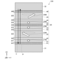
図2は、第1実施形態に係る磁気ヘッドを例示する模式的平面図である。
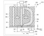
図3は、第1実施形態に磁気ヘッドを含む磁気記録装置を例示する模式的断面図である。
First Embodiment
FIG. 1 is a schematic cross-sectional view illustrating the magnetic head according to the first embodiment.
FIG. 2 is a schematic plan view illustrating the magnetic head according to the first embodiment.
FIG. 3 is a schematic cross-sectional view illustrating a magnetic recording device including the magnetic head according to the first embodiment.
図3に示すように、実施形態に係る磁気記録装置210は、実施形態に係る磁気ヘッド120及び制御部75を含む。磁気記録装置210は、磁気記録媒体80を含んでも良い。磁気記録装置210において、少なくとも記録動作が行われる。記録動作において、磁気ヘッド120を用いて磁気記録媒体80に情報が記録される。
As shown in FIG. 3, the
磁気ヘッド120は、第1磁極31、第2磁極32及び磁気素子20を含む。磁気ヘッド120は、コイル30cを含んで良い。第1磁極31、第2磁極32、磁気素子20及びコイル30cは、記録部60に含まれる。後述するように、磁気ヘッド120は、再生部を含んでも良い。磁気素子20は、第1磁極31と第2磁極32との間に設けられる。
The
例えば、第1磁極31及び第2磁極32は、磁気回路を形成する。第1磁極31は、例えば、主磁極である。第2磁極32は、例えば、トレーリングシールドである。第1磁極31がトレーリングシールドで、第2磁極32が主磁極でも良い。
For example, the first
磁気記録媒体80から磁気ヘッド120への方向をZ軸方向とする。Z軸方向に対して垂直な1つの方向をX軸方向とする。Z軸方向及びX軸方向に対して垂直な方向をY軸方向とする。Z軸方向は、例えばハイト方向に対応する。X軸方向は、例えば、ダウントラック方向に対応する。Y軸方向は、例えば、クロストラック方向に対応する。ダウントラック方向に沿って、磁気記録媒体80と磁気ヘッド120とが相対的に移動する。磁気記録媒体80の所望の位置に、磁気ヘッド120から生じる記録磁界が印加される。磁気記録媒体80の所望の位置の磁化が、記録磁界に応じた方向に制御される。これにより、磁気記録媒体80に情報が記録される。
The direction from the
第1磁極31から第2磁極32への方向を第1方向D1とする。第1方向D1は、実質的にX軸方向に沿う。実施形態において、第1方向D1は、X軸方向に対して傾斜しても良い。傾斜の角度は、例えば、0度を超え30度以下である。
The direction from the first
この例では、コイル30cの一部は、第1磁極31と第2磁極32との間にある。この例では、シールド33が設けられている。X軸方向において、シールド33と第2磁極32との間に第1磁極31がある。コイル30cの別の一部が、シールド33と第1磁極31との間にある。これらの複数の要素の間に、絶縁部30iが設けられる。シールド33は、例えば、リーディングシールドである。磁気ヘッド120は、サイドシールド(図示しない)を含んでも良い。
In this example, a portion of the
図3に示すように、第1磁極31は、媒体対向面30Fを含む。媒体対向面30Fは、例えば、ABS(Air Bearing Surface)である。媒体対向面30Fは、例えば、磁気記録媒体80に対向する。媒体対向面30Fは、例えば、X-Y平面に沿う。
As shown in FIG. 3, the first
図3に示すように、制御部75は、記録回路30D及び素子回路20Dを含む。記録回路30Dから、コイル30cに記録電流Iwが供給される。例えば、第1コイル端子Tc1及び第2コイル端子Tc2がコイル30cに設けられる。これらのコイル端子を介して、記録電流Iwがコイル30cに供給される。第1磁極31から、記録電流Iwに応じた記録磁界が磁気記録媒体80に印加される。
As shown in FIG. 3, the
図3に示すように、素子回路20Dが、磁気素子20に電気的に接続される。この例では、磁気素子20は、第1磁極31及び第2磁極32と電気的に接続される。磁気ヘッド120に、第1端子T1及び第2端子T2が設けられる。第1端子T1は、第1配線W1及び第1磁極31を介して、磁気素子20の一端と電気的に接続される。第2端子T2は、第2配線W2及び第2磁極32を介して、磁気素子20の他端と電気的に接続される。素子回路20Dから、例えば、素子電流icが磁気素子20に供給される。素子電流icは、例えば直流である。
As shown in FIG. 3, the
素子回路20Dは、第1端子T1と第2端子T2との間に素子電圧Ve1を印加する。素子電圧Ve1に基づく素子電流icが、磁気素子20を流れる。
The
例えば、しきい値以上の素子電流icが磁気素子20を流れることで、磁気素子20に含まれる磁性層において発振が生じる。磁気素子20は、例えばSTO(Spin-Torque Oscillator)として機能する。発振に伴い、磁気素子20から交番磁界(例えば高周波磁界)が発生する。磁気素子20で発生した交番磁界が磁気記録媒体80に印加され、磁気記録媒体80への記録がアシストされる。例えば、MAMR(Microwave Assisted Magnetic Recording)が実施可能である。
For example, when an element current ic above a threshold flows through the
上記のように、制御部75は、コイル30cに記録電流Iwを供給し、磁気素子20に素子電流icを供給可能である。
As described above, the
図2は、磁気記録媒体80から媒体対向面30Fをみたときの平面図に対応する。
Figure 2 corresponds to a plan view of the
図1及び図2に示すように、磁気素子20は、第1磁性層21、第2磁性層22、第3磁性層23、第4磁性層24、第5磁性層25、第1非磁性層41、第2非磁性層42、第3非磁性層43、第4非磁性層44、第5非磁性層45及び第6非磁性層46を含む。
As shown in Figures 1 and 2, the
第2磁性層22は、第1磁性層21と第2磁極32との間に設けられる。第3磁性層23は、第2磁性層22と第2磁極32との間に設けられる。第4磁性層24は、第3磁性層23と第2磁極32との間に設けられる。第5磁性層25は、第4磁性層24と第2磁極32との間に設けられる。
The second
第1非磁性層41は、第1磁極31と第1磁性層21との間に設けられる。第2非磁性層42は、第1磁性層21と第2磁性層22との間に設けられる。第3非磁性層43は、第2磁性層22と第3磁性層23との間に設けられる。第4非磁性層44は、第3磁性層23と第4磁性層24との間に設けられる。第5非磁性層45は、第4磁性層24と第5磁性層25との間に設けられる。第6非磁性層46は、第5磁性層25と第2磁極32との間に設けられる。
The first
実施形態において、第6非磁性層46は、Ru、Ir、Ta、Rh、Pd、Pt及びWよりなる群から選択された少なくとも1つを含む。
In an embodiment, the sixth
このような構成により、高い効率で、安定した発振が得られる。実施形態によれば、記録密度の向上が可能な磁気ヘッドを提供できる。以下、磁気素子の特性のシミュレーション結果の例について説明する。 This configuration provides highly efficient and stable oscillation. According to the embodiment, a magnetic head that can improve recording density can be provided. Below, an example of the results of a simulation of the characteristics of the magnetic element is described.
図2に示すように、第1方向D1における第1磁性層21の厚さを第1厚さt21とする。第1方向D1は、第1磁極31から第2磁極32への方向である。第1方向D1における第2磁性層22の厚さを第2厚さt22とする。第1方向D1における第3磁性層23の厚さを第3厚さt23とする。第1方向D1における第4磁性層24の厚さを第4厚さt24とする。第1方向D1における第5磁性層25の厚さを第5厚さt25とする。
As shown in FIG. 2, the thickness of the first
磁気ヘッド120において、第2厚さt22は、第1厚さt21よりも厚い。第2厚さt22は、第3厚さt23よりも厚い。磁気ヘッド120においては、第4厚さt24は、第5厚さt25よりも薄い。
In the
図4は、第1実施形態に係る磁気ヘッドを例示する模式的平面図である。
図4に示すように実施形態に係る磁気ヘッド121も上記の5つの磁性層と、6つの非磁性層と、を含む。磁気ヘッド121においても、第2厚さt22は、第1厚さt21よりも厚い。第2厚さt22は、第3厚さt23よりも厚い。一方、磁気ヘッド121においては、第4厚さt24は、第5厚さt25よりも厚い。このような磁気ヘッド121においても、高い効率で、安定した発振が得られる。
FIG. 4 is a schematic plan view illustrating the magnetic head according to the first embodiment.
As shown in Fig. 4, the
磁極(例えば第2磁極32)の磁化は、必ずしも安定せず、発振する場合がある。このように、第2磁極32の磁化が不安定な場合でも、磁気素子20において、安定した発振が得られることが好ましい。実施形態に係る磁気ヘッド120及び121においては、第2磁極32の磁化が不安定な場合においても、安定した発振が得られる。
The magnetization of the magnetic pole (e.g., the second magnetic pole 32) is not necessarily stable and may oscillate. In this way, even if the magnetization of the second
図5は、参考例の磁気ヘッド例示する模式的平面図である。
図5は、参考例の磁気ヘッド129を示す。磁気ヘッド129においては、磁性層の数が4であり、非磁性層の数が5である。磁気ヘッド129において、第5非磁性層45は、Ru、Ir、Ta、Rh、Pd、Pt及びWよりなる群から選択された少なくとも1つを含む。
FIG. 5 is a schematic plan view illustrating a magnetic head according to a reference example.
5 shows a
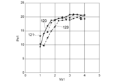
図6は、磁気ヘッドの特性を例示するグラフである。
図6は、磁気ヘッド120、122及び129の特性のシミュレーション結果を例示する。シミュレーションのモデルにおいて、第2磁極32の磁化は、可動である。
FIG. 6 is a graph illustrating the characteristics of the magnetic head.
6 illustrates the results of a simulation of the characteristics of the
図6の横軸は、規格化された印加電圧Vs1である。印加電圧Vs1が、磁気素子20の一端と他端との間に印加される。縦軸は、発振パラメータPo1である。発振パラメータPo1が高い程、高い強度の安定した発振が生じる。
The horizontal axis of FIG. 6 is the normalized applied voltage Vs1. The applied voltage Vs1 is applied between one end and the other end of the
図6に示すように、磁気ヘッド120及び121において、参考例の磁気ヘッド129と比べて、高い発振パラメータPo1が得られる。磁気ヘッド120及び121において、参考例の磁気ヘッド129と比べて、低い印加電圧で高い発振パラメータPo1が得られる。参考例の磁気ヘッド129に含まれる複数の磁性層における厚さの関係を種々に変化させた場合も、その発振パラメータPo1は、磁気ヘッド120及び121における発振パラメータPo1よりも低い。
As shown in FIG. 6, the
磁性層の数が5である構成により、高い強度の発振が得られる。低い素子電圧Ve1(小さい素子電流ic)で、発振が得られる。実施形態によれば、記録密度の向上が可能な磁気ヘッドを提供できる。 A configuration with five magnetic layers provides high-intensity oscillation. Oscillation can be achieved with a low element voltage Ve1 (small element current ic). According to the embodiment, a magnetic head capable of improving recording density can be provided.
上記のように、第6非磁性層46は、Ru、Ir、Ta、Rh、Pd、Pt及びWよりなる群から選択された少なくとも1つを含む。これにより、例えば、第2磁極32の磁化の影響が抑制される。例えば、第4磁性層24または第5磁性層25において、安定した発振が得やすくなる。
As described above, the sixth
実施形態において、例えば、第1非磁性層41は、Ru、Ir、Ta、Rh、Pd、Pt及びWよりなる群から選択された少なくとも1つを含む。例えば、第4非磁性層44は、Ru、Ir、Ta、Rh、Pd、Pt及びWよりなる群から選択された少なくとも1つを含む。
In the embodiment, for example, the first
実施形態において、例えば、第2非磁性層42は、Cu、Au、Cr、Al、V及びAgよりなる群から選択された少なくとも1つを含む。第3非磁性層43は、Cu、Au、Cr、Al、V及びAgよりなる群から選択された少なくとも1つを含む。第5非磁性層45は、Cu、Au、Cr、Al、V及びAgよりなる群から選択された少なくとも1つを含む。
In the embodiment, for example, the second
第1磁性層21、第2磁性層22、第3磁性層23、第4磁性層24及び第5磁性層25の少なくともいずれかは、Fr、Co及びNiよりなる群から選択された少なくとも1つを含む。これらの磁性層は、例えば、強磁性層である。
At least one of the first
図2に例示する磁気ヘッド120において、第2磁性層22及び第5磁性層25は、例えば、発振層として機能する。第1磁性層21、第3磁性層23及び第4磁性層24は、例えば、スピン注入層として機能する。磁気ヘッド120において、例えば、しきい値電圧以上の素子電流icが磁気素子20に流れたときに、第2磁性層22の磁化22M、及び、第5磁性層25の磁化25Mは、発振する。例えば、交番磁界が発生する。
In the
磁気ヘッド120において、例えば、第3磁性層23の磁化23Mの第1方向D1に沿う成分は、第1磁性層21の磁化21Mの第1方向D1に沿う成分に対して反対向きである。第4磁性層24の磁化24Mの第1方向D1に沿う成分は、第3磁性層23の磁化23Mの第1方向D1に沿う成分に対して反対向きである。
In the
図2に示すように、第1方向D1における第1非磁性層41の厚さを第1非磁性層厚さt41とする。第1方向D1における第2非磁性層42の厚さを第2非磁性層厚さt42とする。第1方向D1における第3非磁性層43の厚さを第3非磁性層厚さt43とする。第1方向D1における第4非磁性層44の厚さを第4非磁性層厚さt44とする。第1方向D1における第5非磁性層45の厚さを第5非磁性層厚さt45とする。第1方向D1における第6非磁性層46の厚さを第6非磁性層厚さt46とする。
As shown in FIG. 2, the thickness of the first
磁気ヘッド120において、例えば、第2厚さt22は、第1厚さt21の1.5倍以上10倍以下で良い。第2厚さt22は、第3厚さt23の1.5倍以上10倍以下で良い。第2厚さt22は、第4厚さt24の1.5倍以上10倍以下で良い。例えば、第5厚さt25は、第4厚さt24の1.5倍以上10倍以下で良い。第5厚さt25は、第3厚さt23の1.5倍以上10倍以下で良い。第5厚さt25は、第1厚さt21の1.5倍以上10倍以下で良い。
In the
磁気ヘッド120において、例えば、第1厚さt21は、0.5nm以上5nm以下である。例えば、第2厚さt22は、4nm以上15nm以下である。例えば、第3厚さt23は、0.5nm以上5nm以下である。例えば、第4厚さt24は、0.5nm以上5nm以下である。例えば、第5厚さt25は、4nm以上15nm以下である。
In the
図4に例示する磁気ヘッド121において、第2磁性層22及び第4磁性層24は、例えば、発振層として機能する。第1磁性層21、第3磁性層23及び第5磁性層25は、例えば、スピン注入層として機能する。磁気ヘッド121において、例えば、しきい値電圧以上の素子電流icが磁気素子20に流れたときに、第2磁性層22の磁化22M、及び、第4磁性層24の磁化24Mは、発振する。例えば、交番磁界が発生する。
In the
磁気ヘッド121において、例えば、第3磁性層23の磁化23Mの第1方向D1に沿う成分は、第1磁性層21の磁化21Mの第1方向D1に沿う成分に対して反対向きである。第5磁性層25の磁化25Mの第1方向D1に沿う成分は、第3磁性層23の磁化23Mの第1方向D1に沿う成分と同じ向きである。
In the
磁気ヘッド121において、例えば、第2厚さt22は、第1厚さt21の1.5倍以上10倍以下で良い。第2厚さt22は、第3厚さt23の1.5倍以上10倍以下で良い。例えば、第4厚さt24は、第5厚さt25の1.5倍以上10倍以下で良い。
In the
磁気ヘッド121において、例えば、第1厚さt21は、0.5nm以上5nm以下である。例えば、第2厚さt22は、4nm以上15nm以下である。例えば、第3厚さt23は、0.5nm以上5nm以下である。例えば、第4厚さt24は、4nm以上15nm以下である。例えば、第5厚さt25は、0.5nm以上5nm以下である
磁気ヘッド120及び121において、第1非磁性層厚さt41は、例えば、1nm以上10nm以下で良い。第2非磁性層厚さt42は、例えば、0.5nm以上6nm以下で良い。第3非磁性層厚さt43は、例えば、0.5nm以上6nm以下で良い。第4非磁性層厚さt44は、例えば、1nm以上10nm以下で良い。第5非磁性層厚さt45は、例えば、0.5nm以上6nm以下で良い。第6非磁性層厚さt46は、例えば、1nm以上10nm以下で良い。
In the
図2に示すように、磁気ヘッド120の動作時において、しきい値以上の素子電流icが磁気素子20に供給される。素子電流icは、例えば、第2磁極32から第1磁極31への方向に流れる。素子電流icに対応する電子流jeは、第1磁極31から第2磁極32への方向に流れる。素子電流icは、第6非磁性層46から第1非磁性層41への方向に流れる。
As shown in FIG. 2, when the
動作時において、磁気素子20に素子電圧Ve1が印加される。図2の例では、第1磁極31の電位は、第2磁極32の電位よりも低い。
During operation, an element voltage Ve1 is applied to the
素子電流ic及び素子電圧Ve1は、素子回路20Dにより供給される。例えば、磁気素子20の一端は、第1磁極31に電気的に接続される。磁気素子20の他端は、第2磁極32に電気的に接続される。素子回路20Dは、第1磁極31と第2磁極32との間に素子電圧Ve1を印加可能である。素子電圧Ve1が印加されたときに、第1磁極31の電位は、第2磁極32の電位よりも低い。
The element current ic and the element voltage Ve1 are supplied by the
図4の例では、磁気ヘッド121の動作時において、素子電流icは、例えば、第2磁極32から第1磁極31への方向に流れる。素子電圧Ve1が印加されたときに、第1磁極31の電位は、第2磁極32の電位よりも低い。
In the example of FIG. 4, when the
図7は、第1実施形態に係る磁気ヘッドを例示する模式的平面図である。
図7に示すように、実施形態に係る磁気ヘッド122においては、素子電流icの向きが、磁気ヘッド120における素子電流icの向きと逆である。磁気ヘッド122において、磁気ヘッド121と同様の特性が得られる。
FIG. 7 is a schematic plan view illustrating the magnetic head according to the first embodiment.
7, in the
図8は、第1実施形態に係る磁気ヘッドを例示する模式的平面図である。
図8に示すように、実施形態に係る磁気ヘッド123においては、素子電流icの向きが、磁気ヘッド121における素子電流icの向きと逆である。磁気ヘッド123において、磁気ヘッド120と同様の特性が得られる。
FIG. 8 is a schematic plan view illustrating the magnetic head according to the first embodiment.
8, in the
図9は、第1実施形態に係る磁気ヘッドを例示する模式的平面図である。
図9に示すように、実施形態に係る磁気ヘッド124においては、磁気素子20は、第6磁性層26及び第7非磁性層47をさらに含む。第6磁性層26は、第5磁性層25と第6非磁性層46との間にある。第7非磁性層47は、第5磁性層25と第6磁性層26との間にある。これを除く磁気ヘッド124の構成は、磁気ヘッド120の構成と同様でよい。
FIG. 9 is a schematic plan view illustrating the magnetic head according to the first embodiment.
9 , in the
このような磁気ヘッド124においても、第2磁極32が不安定な場合でも、安定した発振が得られる。磁気ヘッド124において、素子電流icの向きは、第1磁極31から第2磁極32への向きである。
Even with this type of
磁気ヘッド124において、第7非磁性層47は、Cu、Au、Cr、Al、V及びAgよりなる群から選択された少なくとも1つを含む。第1方向D1における第5磁性層25の第5厚さt25は、第1方向D1における第4磁性層24の第4厚さt24よりも厚い。第5厚さt25は、第1方向D1における第6磁性層26の第6厚さt26よりも厚い。
In the
磁気ヘッド124の例において、第6磁性層26の磁化26Mの第1方向D1に沿う成分は、例えば、第4磁性層24の磁化の第1方向D1に沿う成分と反対向きである。磁気ヘッド124において、第6磁性層26は、スピン注入層として機能する。第6磁性層26は、例えば、Fe、Co及びNiよりなる群から選択された少なくとも1つを含む。
In the example of the
第6厚さt26は、例えば、0.5nm以上5nm以下でよい。第1方向D1における第7非磁性層47の第7非磁性層厚さt47は、例えば、0.5nm以上6nm以下で良い。
The sixth thickness t26 may be, for example, 0.5 nm or more and 5 nm or less. The seventh nonmagnetic layer thickness t47 of the seventh
磁気ヘッド124において、第1非磁性層41は、第1磁極31及び第1磁性層21と接する。第2非磁性層42は、第1磁性層21及び第2磁性層22と接する。第3非磁性層43は、第2磁性層22及び第3磁性層23と接する。第4非磁性層44は、第3磁性層23及び第4磁性層24と接する。第5非磁性層45は、第4磁性層24及び第5磁性層25と接する。第7非磁性層47は、第5磁性層25及び第6磁性層26と接する。第6非磁性層46は、第6磁性層26及び第2磁極32と接する。
In the
図10は、第1実施形態に係る磁気ヘッドを例示する模式的平面図である。
図10に示すように、実施形態に係る磁気ヘッド125においては、素子電流icの向きが、磁気ヘッド124における素子電流icの向きと逆である。磁気ヘッド125において、磁気ヘッド124と同様の特性が得られる。
FIG. 10 is a schematic plan view illustrating the magnetic head according to the first embodiment.
10, in the
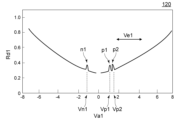
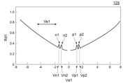
図11は、磁気ヘッドの特性を例示するグラフである。
図11は、磁気ヘッド120に対応する。図11は、磁気素子20に印加される電圧Va1を変化させたときの磁気素子20の微分電気抵抗を例示する。横軸は、電圧Va1である。縦軸は、微分電気抵抗Rd1である。電圧Va1は、第1端子T1と第2端子T2との間の電圧で良い。例えば、電圧Va1に対応する電圧が磁気素子20に印加される。
FIG. 11 is a graph illustrating the characteristics of the magnetic head.
11 corresponds to the
図11に示すように、電圧Va1を変化させたときの微分電気抵抗Rd1は、3以上のピークを含む。これらのピークは、磁気素子20に含まれる複数の磁性層の磁化の反転に伴う電気抵抗の不連続な変化に対応していると考えられる。
As shown in FIG. 11, the differential electrical resistance Rd1 when the voltage Va1 is changed includes three or more peaks. These peaks are considered to correspond to discontinuous changes in electrical resistance caused by magnetization reversals of the multiple magnetic layers included in the
磁気記録装置210(図3参照)は、実施形態に係る磁気ヘッドと、制御部75と、を含む。制御部75は、素子回路20Dを含む。例えば、磁気素子20の一端は、第1磁極31に電気的に接続される。磁気素子20の他端は、第2磁極32に電気的に接続される。
The magnetic recording device 210 (see FIG. 3) includes a magnetic head according to the embodiment and a
図11に示すように、磁気ヘッド120において、第1磁極31と第2磁極32との間の電圧Va1を変化させたときの磁気素子20の微分電気抵抗Rd1は、第1負ピークn1、第1正ピークp1及び第2正ピークp2を含む。第1負ピークn1に対応する電圧Va1は、第1負ピーク電圧Vn1である。第1正ピークp1に対応する電圧Va1は、第1正ピーク電圧Vp1である。第2正ピークp2に対応する電圧Va1は、第2正ピーク電圧Vp2である。
As shown in FIG. 11, in the
第1負ピーク電圧Vn1は負である。第1正ピーク電圧Vp1及び第2正ピーク電圧Vp2は正である。電圧Va1が正のときに、第1磁極31の電位は第2磁極32の電位よりも低い。電圧Va1が負のときに、第1磁極31の電位は第2磁極32の電位よりも高い。
The first negative peak voltage Vn1 is negative. The first positive peak voltage Vp1 and the second positive peak voltage Vp2 are positive. When the voltage Va1 is positive, the potential of the first
第1正ピーク電圧Vp1は、第1負ピーク電圧Vn1よりも高く、第2正ピーク電圧Vp2よりも低い。磁気ヘッド120において、素子電圧Ve1(素子電圧Ve1の絶対値)は、第2正ピーク電圧Vp2以上である。安定で高い強度の発振が得られる。第1負ピーク電圧Vn1の絶対値は、第2正ピーク電圧Vp2よりも大きくても良い。
The first positive peak voltage Vp1 is higher than the first negative peak voltage Vn1 and lower than the second positive peak voltage Vp2. In the
このように、微分電気抵抗Rd1は、3つ以上のピーク(例えば、第1ピーク、第2ピーク及び第3ピーク)を含む。「第1ピーク」は、例えば、第1負ピークn1である。「第2ピーク」は、例えば、第1正ピークp1である。「第3ピーク」は、例えば、第2正ピークp2である。第1負ピーク電圧Vn1は、例えば第1電圧である。第1正ピーク電圧Vp1は、例えば第2電圧である。第2正ピーク電圧Vp2は、例えば、第3電圧である。第2電圧は、第1電圧と第3電圧との間である。素子電圧Ve1は、第3電圧以上である。 Thus, the differential electrical resistance Rd1 includes three or more peaks (e.g., a first peak, a second peak, and a third peak). The "first peak" is, for example, the first negative peak n1. The "second peak" is, for example, the first positive peak p1. The "third peak" is, for example, the second positive peak p2. The first negative peak voltage Vn1 is, for example, the first voltage. The first positive peak voltage Vp1 is, for example, the second voltage. The second positive peak voltage Vp2 is, for example, the third voltage. The second voltage is between the first voltage and the third voltage. The element voltage Ve1 is equal to or greater than the third voltage.
このように、素子電圧Ve1は、第1条件を満たして良い。第1条件において、第1電圧は負である。第2電圧、第3電圧及び素子電圧Ve1は正である。第1条件において、素子電圧Ve1は、第3電圧以上である。 In this way, the element voltage Ve1 may satisfy the first condition. In the first condition, the first voltage is negative. The second voltage, the third voltage, and the element voltage Ve1 are positive. In the first condition, the element voltage Ve1 is equal to or greater than the third voltage.
磁気ヘッド120において、例えば、素子電圧Ve1の絶対値は、第1正ピーク電圧Vp1の絶対値の10倍以下で良い。例えば、素子電圧Ve1の絶対値は、第1正ピーク電圧Vp1の絶対値の8倍以下でも良い。例えば、素子電圧Ve1の絶対値は、第1負ピーク電圧Vn1の絶対値の10倍以下で良い。例えば、素子電圧Ve1の絶対値は、第1負ピーク電圧Vn1の絶対値の8倍以下でも良い。
In the
磁気ヘッド120において、例えば、第3電圧の絶対値は、第1正ピーク電圧Vp1の絶対値の4倍以下で良い。例えば、第3電圧の絶対値は、第1正ピーク電圧Vp1の絶対値の3倍以下でも良い。例えば、第3電圧の絶対値は、第1負ピーク電圧Vn1の絶対値の4倍以下で良い。例えば、第3電圧の絶対値は、第1負ピーク電圧Vn1の絶対値の3倍以下でも良い。
In the
磁気ヘッド120において、第1正ピークp1のテールが第2正ピークp2と重なっても良い。第2正ピークp2のテールが第1正ピークp1と重なっても良い。
In the
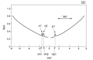
図12は、磁気ヘッドの特性を例示するグラフである。
図12は、磁気ヘッド121に対応する。図12に示すように、磁気ヘッド121において、電圧Va1を変化させたときの磁気素子20の微分電気抵抗Rd1は、第1負ピークn1、第2負ピークn2及び第1正ピークp1を含む。第1負ピークn1に対応する電圧Va1は、第1負ピーク電圧Vn1である。第2負ピークn2に対応する電圧Va1は、第2負ピーク電圧Vn2である。第1正ピークp1に対応する電圧Va1は、第1正ピーク電圧Vp1である。
FIG. 12 is a graph illustrating the characteristics of the magnetic head.
Fig. 12 corresponds to the
第1負ピーク電圧Vn1及び第2負ピーク電圧Vn2は負である。第1正ピーク電圧Vp1は正である。第2負ピーク電圧Vn2は、第1負ピーク電圧Vn1よりも高く、第1正ピーク電圧Vp1よりも低い。磁気ヘッド121において、素子電圧Ve1は、第1正ピーク電圧Vp1以上である。安定で高い強度の発振が得られる。
The first negative peak voltage Vn1 and the second negative peak voltage Vn2 are negative. The first positive peak voltage Vp1 is positive. The second negative peak voltage Vn2 is higher than the first negative peak voltage Vn1 and lower than the first positive peak voltage Vp1. In the
磁気ヘッド121において、「第1ピーク」は、例えば、第1負ピークn1である。「第2ピーク」は、例えば、第2負ピークn2である。「第3ピーク」は、例えば、第1正ピークp1である。第1負ピーク電圧Vn1は、例えば第1電圧である。第2負ピーク電圧Vn2は、例えば第2電圧である。第1正ピーク電圧Vp1は、例えば、第3電圧である。第2電圧は、第1電圧と第3電圧との間である。素子電圧Ve1は、第3電圧以上である。
In the
このように、素子電圧Ve1は、第2条件を満たして良い。第2条件において、第1電圧及び第2電圧は負である。第3電圧及び素子電圧は正である。第3条件において、素子電圧Ve1は、第3電圧以上である。 In this way, the element voltage Ve1 may satisfy the second condition. In the second condition, the first voltage and the second voltage are negative. The third voltage and the element voltage are positive. In the third condition, the element voltage Ve1 is equal to or greater than the third voltage.
磁気ヘッド121において、例えば、素子電圧Ve1の絶対値は、第1正ピーク電圧Vp1の絶対値の10倍以下で良い。素子電圧Ve1の絶対値は、第1正ピーク電圧Vp1の絶対値の8倍以下でも良い。磁気ヘッド121において、例えば、素子電圧Ve1の絶対値は、第2負ピーク電圧Vn2の絶対値の10倍以下で良い。素子電圧Ve1の絶対値は、第2負ピーク電圧Vn2の絶対値の8倍以下でも良い。
In the
磁気ヘッド121において、例えば、第3電圧の絶対値は、第1負ピーク電圧Vn1の絶対値の4倍以下で良い。例えば、第3電圧の絶対値は、第1負ピーク電圧Vn1の絶対値の3倍以下でも良い。例えば、第3電圧の絶対値は、第2負ピーク電圧Vn2の絶対値の4倍以下で良い。例えば、第3電圧の絶対値は、第2負ピーク電圧Vn2の絶対値の3倍以下でも良い。
In the
磁気ヘッド121において、第1負ピークn1のテールが第2負ピークn2と重なっても良い。第2負ピークn2のテールが第1負ピークn1と重なっても良い。
In the
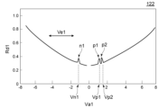
図13は、磁気ヘッドの特性を例示するグラフである。
図13は、磁気ヘッド122に対応する。図13に示すように、磁気ヘッド122において、電圧Va1を変化させたときの磁気素子20の微分電気抵抗Rd1は、第1負ピークn1、第1正ピークp1及び第2正ピークp2を含む。第1正ピーク電圧Vp1は、第1負ピーク電圧Vn1よりも高く、第2正ピーク電圧Vp2よりも低い。磁気ヘッド122において、負の素子電圧Ve1の絶対値は、第1負ピーク電圧Vn1の絶対値以上である。安定で高い強度の発振が得られる。第1負ピーク電圧Vn1の絶対値は、第2正ピーク電圧Vp2よりも大きくても良い。
FIG. 13 is a graph illustrating the characteristics of the magnetic head.
13 corresponds to the
このように、微分電気抵抗Rd1は、3つ以上のピーク(例えば、第1ピーク、第2ピーク及び第3ピーク)を含む。「第1ピーク」は、例えば、第1負ピークn1である。「第2ピーク」は、例えば、第1正ピークp1である。「第3ピーク」は、例えば、第2正ピークp2である。第1負ピーク電圧Vn1は、例えば第1電圧である。第1正ピーク電圧Vp1は、例えば第2電圧である。第2正ピーク電圧Vp2は、例えば、第3電圧である。第2電圧は、第1電圧と第3電圧との間である。負の素子電圧Ve1の絶対値は、第1電圧の絶対値以上である。 Thus, the differential electrical resistance Rd1 includes three or more peaks (e.g., a first peak, a second peak, and a third peak). The "first peak" is, for example, the first negative peak n1. The "second peak" is, for example, the first positive peak p1. The "third peak" is, for example, the second positive peak p2. The first negative peak voltage Vn1 is, for example, the first voltage. The first positive peak voltage Vp1 is, for example, the second voltage. The second positive peak voltage Vp2 is, for example, the third voltage. The second voltage is between the first voltage and the third voltage. The absolute value of the negative element voltage Ve1 is greater than or equal to the absolute value of the first voltage.
このように、素子電圧Ve1は、第3条件を満たして良い。第3条件において、第1電圧及び素子電圧Ve1は負である。第2電圧及び第3電圧は正である。第3条件において、素子電圧Ve1の絶対値は、第1電圧の絶対値以上である。 In this way, the element voltage Ve1 may satisfy the third condition. In the third condition, the first voltage and the element voltage Ve1 are negative. The second voltage and the third voltage are positive. In the third condition, the absolute value of the element voltage Ve1 is greater than or equal to the absolute value of the first voltage.
磁気ヘッド122において、例えば、素子電圧Ve1の絶対値は、第1負ピーク電圧Vn1の絶対値の10倍以下で良い。例えば、素子電圧Ve1の絶対値は、第1負ピーク電圧Vn1の絶対値の8倍以下でも良い。例えば、素子電圧Ve1の絶対値は、第1正ピーク電圧Vp1の絶対値の10倍以下で良い。例えば、素子電圧Ve1の絶対値は、第1正ピーク電圧Vp1の絶対値の8倍以下でも良い。
In the
磁気ヘッド122において、例えば、第1電圧の絶対値は、第1正ピーク電圧Vp1の絶対値の4倍以下で良い。例えば、第1電圧の絶対値は、第1正ピーク電圧Vp1の絶対値の3倍以下でも良い。例えば、第1電圧の絶対値は、第2正ピーク電圧Vp2の絶対値の4倍以下で良い。例えば、第1電圧の絶対値は、第2正ピーク電圧Vp2の絶対値の3倍以下でも良い。
In the
図14は、磁気ヘッドの特性を例示するグラフである。
図14は、磁気ヘッド123に対応する。図14に示すように、磁気ヘッド123において、電圧Va1を変化させたときの磁気素子20の微分電気抵抗Rd1は、第1負ピークn1、第2負ピークn2及び第1正ピークp1を含む。第1負ピークn1に対応する電圧Va1は、第1負ピーク電圧Vn1である。第2負ピークn2に対応する電圧Va1は、第2負ピーク電圧Vn2である。第1正ピークp1に対応する電圧Va1は、第1正ピーク電圧Vp1である。
FIG. 14 is a graph illustrating the characteristics of the magnetic head.
Fig. 14 corresponds to the
第1負ピーク電圧Vn1及び第2負ピーク電圧Vn2は負である。第1正ピーク電圧Vp1は正である。第2負ピーク電圧Vn2は、第1負ピーク電圧Vn1よりも高く、第1正ピーク電圧Vp1よりも低い。磁気ヘッド123において、負の素子電圧Ve1の絶対値は、負の第1負ピーク電圧Vn1の絶対値以上である。安定で高い強度の発振が得られる。
The first negative peak voltage Vn1 and the second negative peak voltage Vn2 are negative. The first positive peak voltage Vp1 is positive. The second negative peak voltage Vn2 is higher than the first negative peak voltage Vn1 and lower than the first positive peak voltage Vp1. In the
磁気ヘッド123において、「第1ピーク」は、例えば、第1負ピークn1である。「第2ピーク」は、例えば、第2負ピークn2である。「第3ピーク」は、例えば、第1正ピークp1である。第1負ピーク電圧Vn1は、例えば第1電圧である。第2負ピーク電圧Vn2は、例えば第2電圧である。第1正ピーク電圧Vp1は、例えば、第3電圧である。第2電圧は、第1電圧と第3電圧との間である。負の素子電圧Ve1の絶対値は、負の第1電圧の絶対値以上である。
In the
このように、素子電圧Ve1は、第4条件を満たして良い。第4条件において、第1電圧、第2電圧及び素子電圧Ve1は負である。第3電圧は正である。第4条件において、素子電圧Ve1の絶対値は、第1電圧の絶対値以上である。 In this way, the element voltage Ve1 may satisfy the fourth condition. In the fourth condition, the first voltage, the second voltage, and the element voltage Ve1 are negative. The third voltage is positive. In the fourth condition, the absolute value of the element voltage Ve1 is greater than or equal to the absolute value of the first voltage.
磁気ヘッド123において、例えば、素子電圧Ve1の絶対値は、第2負ピーク電圧Vn2の絶対値の10倍以下で良い。素子電圧Ve1の絶対値は、第2負ピーク電圧Vn2の絶対値の8倍以下でも良い。例えば、素子電圧Ve1の絶対値は、第1正ピーク電圧Vp1の絶対値の10倍以下で良い。素子電圧Ve1の絶対値は、第1正ピーク電圧Vp1の絶対値の8倍以下でも良い。
In the
磁気ヘッド123において、例えば、第1電圧の絶対値は、第1正ピーク電圧Vp1の絶対値の4倍以下で良い。例えば、第1電圧の絶対値は、第1正ピーク電圧Vp1の絶対値の3倍以下でも良い。例えば、第1電圧の絶対値は、第2負ピーク電圧Vn2の絶対値の4倍以下で良い。例えば、第1電圧の絶対値は、第2負ピーク電圧Vn2の絶対値の3倍以下でも良い。
In the
磁気ヘッド123において、第1負ピークn1のテールが第2負ピークn2と重なっても良い。第2負ピークn2のテールが第1負ピークn1と重なっても良い。
In the
図15は、磁気ヘッドの特性を例示するグラフである。
図15は、磁気ヘッド124に対応する。図15に示すように、磁気ヘッド124において、電圧Va1を変化させたときの磁気素子20の微分電気抵抗Rd1は、第1負ピークn1、第2負ピークn2、第1正ピークp1及び第2正ピークp2を含む。第1負ピークn1に対応する電圧Va1は、負の第1負ピーク電圧Vn1である。第2負ピークn2に対応する電圧Va1は、負の第2負ピーク電圧Vn2である。第1正ピークp1に対応する電圧Va1は、正の第1正ピーク電圧Vp1である。第2正ピークp2に対応する電圧Va1は、正の第2正ピーク電圧Vp2である。第2負ピーク電圧Vn2は、第1負ピーク電圧Vn1と第2正ピーク電圧Vp2との間である。第1正ピーク電圧Vp1は、第2負ピーク電圧Vn2と第2正ピーク電圧Vp2との間である。
FIG. 15 is a graph illustrating the characteristics of the magnetic head.
15 corresponds to the
素子電圧Ve1は、第5条件を満たす。第5条件において、素子電圧Ve1は正である。第5条件において、素子電圧Ve1は、第2正ピーク電圧Vp2以上である。安定で高い強度の発振が得られる。 The element voltage Ve1 satisfies the fifth condition. In the fifth condition, the element voltage Ve1 is positive. In the fifth condition, the element voltage Ve1 is equal to or greater than the second positive peak voltage Vp2. A stable, high-intensity oscillation is obtained.
磁気ヘッド124において、例えば、素子電圧Ve1の絶対値は、第1正ピーク電圧Vp1の絶対値の10倍以下で良い。素子電圧Ve1の絶対値は、第1正ピーク電圧Vp1の絶対値の8倍以下でも良い。例えば、素子電圧Ve1の絶対値は、第2負ピーク電圧Vn2の絶対値の10倍以下で良い。素子電圧Ve1の絶対値は、第2負ピーク電圧Vn2の絶対値の8倍以下でも良い。
In the
磁気ヘッド124において、例えば、第2正ピーク電圧Vp2の絶対値は、第1正ピーク電圧Vp1の絶対値の4倍以下で良い。例えば、第2正ピーク電圧Vp2の絶対値は、第1正ピーク電圧Vp1の絶対値の3倍以下でも良い。例えば、第2正ピーク電圧Vp2の絶対値は、第2負ピーク電圧Vn2の絶対値の4倍以下で良い。例えば、第2正ピーク電圧Vp2の絶対値は、第2負ピーク電圧Vn2の絶対値の3倍以下でも良い。
In the
図16は、磁気ヘッドの特性を例示するグラフである。
図16は、磁気ヘッド125に対応する。図16に示すように、磁気ヘッド125において、電圧Va1を変化させたときの磁気素子20の微分電気抵抗Rd1は、第1負ピークn1、第2負ピークn2、第1正ピークp1及び第2正ピークp2を含む。第1負ピークn1に対応する電圧Va1は、負の第1負ピーク電圧Vn1である。第2負ピークn2に対応する電圧Va1は、負の第2負ピーク電圧Vn2である。第1正ピークp1に対応する電圧Va1は、正の第1正ピーク電圧Vp1である。第2正ピークp2に対応する電圧Va1は、正の第2正ピーク電圧Vp2である。
FIG. 16 is a graph illustrating the characteristics of the magnetic head.
16 corresponds to the
素子電圧Ve1は、第6条件を満たす。第6条件において、素子電圧Ve1は負である。第6条件において、素子電圧Ve1の絶対値は、第1負ピーク電圧Vn1の絶対値以上である。安定で高い強度の発振が得られる。 The element voltage Ve1 satisfies the sixth condition. In the sixth condition, the element voltage Ve1 is negative. In the sixth condition, the absolute value of the element voltage Ve1 is equal to or greater than the absolute value of the first negative peak voltage Vn1. A stable, high-intensity oscillation is obtained.
磁気ヘッド125において、例えば、素子電圧Ve1の絶対値は、第1正ピーク電圧Vp1の絶対値の10倍以下で良い。素子電圧Ve1の絶対値は、第1正ピーク電圧Vp1の絶対値の8倍以下でも良い。例えば、素子電圧Ve1の絶対値は、第2負ピーク電圧Vn2の絶対値の10倍以下で良い。素子電圧Ve1の絶対値は、第2負ピーク電圧Vn2の絶対値の8倍以下でも良い。
In the
磁気ヘッド125において、例えば、第1負ピーク電圧Vn1の絶対値は、第1正ピーク電圧Vp1の絶対値の4倍以下で良い。例えば、第1負ピーク電圧Vn1の絶対値は、第1正ピーク電圧Vp1の絶対値の3倍以下でも良い。例えば、第1負ピーク電圧Vn1の絶対値は、第2負ピーク電圧Vn2の絶対値の4倍以下で良い。例えば、第1負ピーク電圧Vn1の絶対値は、第2負ピーク電圧Vn2の絶対値の3倍以下でも良い。
In the
磁気ヘッド124及び磁気ヘッド125において、第1正ピークp1のテールが第2正ピークp2と重なっても良い。第2正ピークp2のテールが第1正ピークp1と重なっても良い。第1負ピークn1のテールが第2負ピークn2と重なっても良い。第2負ピークn2のテールが第1負ピークn1と重なっても良い。
In
実施形態において、第1磁極31は、X軸方向に沿って並ぶ複数の磁性領域を含んでも良い。第2磁極32は、X軸方向に沿って並ぶ複数の磁性領域を含んでも良い。複数の磁性領域の間の境界は、明確でも不明確でも良い。例えば、複数の磁性領域は、連続している。
In an embodiment, the first
以下、実施形態に係る磁気記録装置に関する他の構成の例について説明する。以下では、磁気ヘッド120が用いられる例について説明する。以下の説明において、「磁気ヘッド」は、実施形態に係る任意の磁気ヘッド(及びその変形)で良い。
Other examples of configurations of the magnetic recording device according to the embodiment will be described below. Below, an example in which the
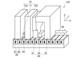
図17は、実施形態に係る磁気記録装置を例示する模式的斜視図である。
図17に示すように、実施形態に係る磁気ヘッド(例えば、磁気ヘッド120)は、磁気記録媒体80と共に用いられる。この例では、磁気ヘッド120は、記録部60及び再生部70を含む。磁気ヘッド120の記録部60により、磁気記録媒体80に情報が記録される。再生部70により、磁気記録媒体80に記録された情報が再生される。
FIG. 17 is a schematic perspective view illustrating the magnetic recording device according to the embodiment.
17 , a magnetic head according to an embodiment (e.g., magnetic head 120) is used together with a
磁気記録媒体80は、例えば、媒体基板82と、媒体基板82の上に設けられた磁気記録層81と、を含む。磁気記録層81の磁化83が記録部60により制御される。
The
再生部70は、例えば、第1再生磁気シールド72a、第2再生磁気シールド72b、及び磁気再生素子71を含む。磁気再生素子71は、第1再生磁気シールド72aと第2再生磁気シールド72bとの間に設けられる。磁気再生素子71は、磁気記録層81の磁化83に応じた信号を出力可能である。
The reproducing
図17に示すように、磁気記録媒体80は、媒体移動方向85の方向に、磁気ヘッド120に対して相対的に移動する。磁気ヘッド120により、任意の位置において、磁気記録層81の磁化83に対応する情報が制御される。磁気ヘッド120により、任意の位置において、磁気記録層81の磁化83に対応する情報が再生される。
As shown in FIG. 17, the
図18は、実施形態に係る磁気記録装置の一部を例示する模式的斜視図である。
図18は、ヘッドスライダを例示している。
磁気ヘッド120は、ヘッドスライダ159に設けられる。ヘッドスライダ159は、例えばAl2O3/TiCなどを含む。ヘッドスライダ159は、磁気記録媒体の上を、浮上または接触しながら、磁気記録媒体に対して相対的に運動する。
FIG. 18 is a schematic perspective view illustrating a portion of the magnetic recording device according to the embodiment.
FIG. 18 illustrates a head slider.
The
ヘッドスライダ159は、例えば、空気流入側159A及び空気流出側159Bを有する。磁気ヘッド120は、ヘッドスライダ159の空気流出側159Bの側面などに配置される。これにより、磁気ヘッド120は、磁気記録媒体の上を浮上または接触しながら磁気記録媒体に対して相対的に運動する。
The
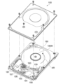
図19は、実施形態に係る磁気記録装置を例示する模式的斜視図である。
図20(a)及び図20(b)は、実施形態に係る磁気記録装置の一部を例示する模式的斜視図である。
図19に示すように、実施形態に係る磁気記録装置150においては、ロータリーアクチュエータが用いられる。記録用媒体ディスク180は、スピンドルモータ180Mに装着される。記録用媒体ディスク180は、スピンドルモータ180Mにより矢印ARの方向に回転する。スピンドルモータ180Mは、駆動装置制御部からの制御信号に応答する。本実施形態に係る磁気記録装置150は、複数の記録用媒体ディスク180を備えても良い。磁気記録装置150は、記録媒体181を含んでもよい。記録媒体181は、例えば、SSD(Solid State Drive)である。記録媒体181には、例えば、フラッシュメモリなどの不揮発性メモリが用いられる。例えば、磁気記録装置150は、ハイブリッドHDD(Hard Disk Drive)でも良い。
FIG. 19 is a schematic perspective view illustrating the magnetic recording device according to the embodiment.
20A and 20B are schematic perspective views illustrating a portion of the magnetic recording device according to the embodiment.
As shown in FIG. 19, a rotary actuator is used in the
ヘッドスライダ159は、記録用媒体ディスク180に記録する情報の、記録及び再生を行う。ヘッドスライダ159は、薄膜状のサスペンション154の先端に設けられる。ヘッドスライダ159の先端付近に、実施形態に係る磁気ヘッドが設けられる。
The
記録用媒体ディスク180が回転すると、サスペンション154による押し付け圧力と、ヘッドスライダ159の媒体対向面(ABS)で発生する圧力と、がバランスする。ヘッドスライダ159の媒体対向面と、記録用媒体ディスク180の表面と、の間の距離が、所定の浮上量となる。実施形態において、ヘッドスライダ159は、記録用媒体ディスク180と接触しても良い。例えば、接触走行型が適用されても良い。
When the
サスペンション154は、アーム155(例えばアクチュエータアーム)の一端に接続されている。アーム155は、例えば、ボビン部などを有する。ボビン部は、駆動コイルを保持する。アーム155の他端には、ボイスコイルモータ156が設けられる。ボイスコイルモータ156は、リニアモータの一種である。ボイスコイルモータ156は、例えば、駆動コイル及び磁気回路を含む。駆動コイルは、アーム155のボビン部に巻かれる。磁気回路は、永久磁石及び対向ヨークを含む。永久磁石と対向ヨークとの間に、駆動コイルが設けられる。サスペンション154は、一端と他端とを有する。磁気ヘッドは、サスペンション154の一端に設けられる。アーム155は、サスペンション154の他端に接続される。
The
アーム155は、ボールベアリングによって保持される。ボールベアリングは、軸受部157の上下の2箇所に設けられる。アーム155は、ボイスコイルモータ156により回転及びスライドが可能である。磁気ヘッドは、記録用媒体ディスク180の任意の位置に移動可能である。
The
図20(a)は、磁気記録装置の一部の構成を例示しており、ヘッドスタックアセンブリ160の拡大斜視図である。
図20(b)は、ヘッドスタックアセンブリ160の一部となる磁気ヘッドアセンブリ(ヘッドジンバルアセンブリ:HGA)158を例示する斜視図である。
FIG. 20A illustrates a partial configuration of the magnetic recording device, and is an enlarged perspective view of a
FIG. 20B is a perspective view illustrating a magnetic head assembly (head gimbal assembly: HGA) 158 which is a part of the
図20(a)に示すように、ヘッドスタックアセンブリ160は、軸受部157と、ヘッドジンバルアセンブリ158と、支持フレーム161と、を含む。ヘッドジンバルアセンブリ158は、軸受部157から延びる。支持フレーム161は、軸受部157から延びる。支持フレーム161の延びる方向は、ヘッドジンバルアセンブリ158の延びる方向とは逆である。支持フレーム161は、ボイスコイルモータ156のコイル162を支持する。
As shown in FIG. 20(a), the
図20(b)に示すように、ヘッドジンバルアセンブリ158は、軸受部157から延びたアーム155と、アーム155から延びたサスペンション154と、を有している。
As shown in FIG. 20(b), the
サスペンション154の先端には、ヘッドスライダ159が設けられる。ヘッドスライダ159に、実施形態に係る磁気ヘッドが設けられる。
A
実施形態に係る磁気ヘッドアセンブリ(ヘッドジンバルアセンブリ)158は、実施形態に係る磁気ヘッドと、磁気ヘッドが設けられたヘッドスライダ159と、サスペンション154と、アーム155と、を含む。ヘッドスライダ159は、サスペンション154の一端に設けられる。アーム155は、サスペンション154の他端と接続される。
The magnetic head assembly (head gimbal assembly) 158 according to the embodiment includes the magnetic head according to the embodiment, a
サスペンション154は、例えば、信号の記録及び再生用のリード線(図示しない)を有する。サスペンション154は、例えば、浮上量調整のためのヒーター用のリード線(図示しない)を有しても良い。サスペンション154は、例えば発振素子などのためのリード線(図示しない)を有しても良い。これらのリード線と、磁気ヘッドに設けられた複数の電極と、が電気的に接続される。
The
磁気記録装置150において、信号処理部190が設けられる。信号処理部190は、磁気ヘッドを用いて磁気記録媒体への信号の記録及び再生を行う。信号処理部190は、信号処理部190の入出力線は、例えば、ヘッドジンバルアセンブリ158の電極パッドに接続され、磁気ヘッドと電気的に接続される。
A
実施形態に係る磁気記録装置150は、磁気記録媒体と、実施形態に係る磁気ヘッドと、可動部と、位置制御部と、信号処理部と、を含む。可動部は、磁気記録媒体と磁気ヘッドとを離間させ、または、接触させた状態で相対的に移動可能とする。位置制御部は、磁気ヘッドを磁気記録媒体の所定記録位置に位置合わせする。信号処理部は、磁気ヘッドを用いた磁気記録媒体への信号の記録及び再生を行う。
The
例えば、上記の磁気記録媒体として、記録用媒体ディスク180が用いられる。上記の可動部は、例えば、ヘッドスライダ159を含む。上記の位置制御部は、例えば、ヘッドジンバルアセンブリ158を含む。
For example, a
実施形態は、以下の構成(例えば技術案)を含んでも良い。
(構成1)
第1磁極と、
第2磁極と、
前記第1磁極と前記第2磁極との間に設けられた磁気素子と、
を備え、
前記磁気素子は、
第1磁性層と、
前記第1磁性層と前記第2磁極との間に設けられた第2磁性層と、
前記第2磁性層と前記第2磁極との間に設けられた第3磁性層と、
前記第3磁性層と前記第2磁極との間に設けられた第4磁性層と、
前記第4磁性層と前記第2磁極との間に設けられた第5磁性層と、
前記第1磁極と前記第1磁性層との間に設けられた第1非磁性層と、
前記第1磁性層と前記第2磁性層との間に設けられた第2非磁性層と、
前記第2磁性層と前記第3磁性層との間に設けられた第3非磁性層と、
前記第3磁性層と前記第4磁性層との間に設けられた第4非磁性層と、
前記第4磁性層と前記第5磁性層との間に設けられた第5非磁性層と、
前記第5磁性層と前記第2磁極との間に設けられた第6非磁性層と、
を含み、
前記第6非磁性層は、Ru、Ir、Ta、Rh、Pd、Pt及びWよりなる群から選択された少なくとも1つを含む、磁気ヘッド。
The embodiment may include the following configurations (e.g., technical solutions).
(Configuration 1)
A first magnetic pole;
A second magnetic pole;
a magnetic element provided between the first magnetic pole and the second magnetic pole;
Equipped with
The magnetic element includes:
A first magnetic layer;
a second magnetic layer provided between the first magnetic layer and the second magnetic pole;
a third magnetic layer provided between the second magnetic layer and the second magnetic pole;
a fourth magnetic layer provided between the third magnetic layer and the second magnetic pole;
a fifth magnetic layer provided between the fourth magnetic layer and the second magnetic pole;
a first nonmagnetic layer provided between the first magnetic pole and the first magnetic layer;
a second nonmagnetic layer provided between the first magnetic layer and the second magnetic layer;
a third nonmagnetic layer provided between the second magnetic layer and the third magnetic layer;
a fourth nonmagnetic layer provided between the third magnetic layer and the fourth magnetic layer;
a fifth nonmagnetic layer provided between the fourth magnetic layer and the fifth magnetic layer;
a sixth nonmagnetic layer provided between the fifth magnetic layer and the second magnetic pole;
Including,
The sixth nonmagnetic layer includes at least one selected from the group consisting of Ru, Ir, Ta, Rh, Pd, Pt, and W.
(構成2)
前記第1非磁性層は、Ru、Ir、Ta、Rh、Pd、Pt及びWよりなる群から選択された少なくとも1つを含み、
前記第4非磁性層は、Ru、Ir、Ta、Rh、Pd、Pt及びWよりなる群から選択された少なくとも1つを含む、構成1に記載の磁気ヘッド。
(Configuration 2)
the first nonmagnetic layer includes at least one selected from the group consisting of Ru, Ir, Ta, Rh, Pd, Pt, and W;
2. The magnetic head of
(構成3)
前記第2非磁性層は、Cu、Au、Cr、Al、V及びAgよりなる群から選択された少なくとも1つを含み、
前記第3非磁性層は、Cu、Au、Cr、Al、V及びAgよりなる群から選択された少なくとも1つを含み、
前記第5非磁性層は、Cu、Au、Cr、Al、V及びAgよりなる群から選択された少なくとも1つを含む、構成2に記載の磁気ヘッド。
(Configuration 3)
the second nonmagnetic layer includes at least one selected from the group consisting of Cu, Au, Cr, Al, V, and Ag;
the third nonmagnetic layer includes at least one selected from the group consisting of Cu, Au, Cr, Al, V, and Ag;
3. The magnetic head of
(構成4)
前記第1磁極から前記第2磁極への第1方向における前記第2磁性層の第2厚さは、前記第1方向における前記第1磁性層の第1厚さよりも厚く、
前記第2厚さは、前記第1方向における前記第3磁性層の第3厚さよりも厚い、構成3に記載の磁気ヘッド。
(Configuration 4)
a second thickness of the second magnetic layer in a first direction from the first magnetic pole to the second magnetic pole is greater than a first thickness of the first magnetic layer in the first direction;
4. The magnetic head of
(構成5)
前記第1方向における前記第4磁性層の第4厚さは、前記第1方向における前記第5磁性層の第5厚さよりも薄い、構成4に記載の磁気ヘッド。
(Configuration 5)
5. The magnetic head of
(構成6)
前記第1方向における前記第4磁性層の第4厚さは、前記第1方向における前記第5磁性層の第5厚さよりも厚い、構成4に記載の磁気ヘッド。
(Configuration 6)
5. The magnetic head of
(構成7)
前記磁気素子は、
第6磁性層と、
第7非磁性層と、
をさらに含み、
前記第6磁性層は、前記第5磁性層と前記第6非磁性層との間にあり、
前記第7非磁性層は、前記第5磁性層と前記第6磁性層との間にある、構成4に記載の磁気ヘッド。
(Configuration 7)
The magnetic element includes:
A sixth magnetic layer;
A seventh nonmagnetic layer;
Further comprising:
the sixth magnetic layer is between the fifth magnetic layer and the sixth nonmagnetic layer,
5. The magnetic head of
(構成8)
前記第7非磁性層は、Cu、Au、Cr、Al、V及びAgよりなる群から選択された少なくとも1つを含み、
前記第1方向における前記第5磁性層の第5厚さは、前記第1方向における前記第4磁性層の第4厚さよりも厚く、
前記第5厚さは、前記第1方向における前記第6磁性層の第6厚さよりも厚い、構成7に記載の磁気ヘッド。
(Configuration 8)
the seventh nonmagnetic layer includes at least one selected from the group consisting of Cu, Au, Cr, Al, V, and Ag;
a fifth thickness of the fifth magnetic layer in the first direction is greater than a fourth thickness of the fourth magnetic layer in the first direction;
8. The magnetic head of claim 7, wherein the fifth thickness is greater than a sixth thickness of the sixth magnetic layer in the first direction.
(構成9)
前記第1非磁性層は、前記第1磁極及び前記第1磁性層と接し、
前記第2非磁性層は、前記第1磁性層及び前記第2磁性層と接し、
前記第3非磁性層は、前記第2磁性層及び前記第3磁性層と接し、
前記第4非磁性層は、前記第3磁性層及び前記第4磁性層と接し、
前記第5非磁性層は、前記第4磁性層及び前記第5磁性層と接し、
前記第7非磁性層は、前記第5磁性層及び前記第6磁性層と接し、
前記第6非磁性層は、前記第6磁性層及び前記第2磁極と接する、構成8に記載の磁気ヘッド。
(Configuration 9)
the first nonmagnetic layer is in contact with the first magnetic pole and the first magnetic layer,
the second nonmagnetic layer is in contact with the first magnetic layer and the second magnetic layer,
the third nonmagnetic layer is in contact with the second magnetic layer and the third magnetic layer,
the fourth nonmagnetic layer is in contact with the third magnetic layer and the fourth magnetic layer,
the fifth nonmagnetic layer is in contact with the fourth magnetic layer and the fifth magnetic layer,
the seventh nonmagnetic layer is in contact with the fifth magnetic layer and the sixth magnetic layer,
9. The magnetic head of
(構成10)
前記第1非磁性層は、前記第1磁極及び前記第1磁性層と接し、
前記第2非磁性層は、前記第1磁性層及び前記第2磁性層と接し、
前記第3非磁性層は、前記第2磁性層及び前記第3磁性層と接し、
前記第4非磁性層は、前記第3磁性層及び前記第4磁性層と接し、
前記第5非磁性層は、前記第4磁性層及び前記第5磁性層と接し、
前記第6非磁性層は、前記第5磁性層及び前記第2磁極と接する、構成4に記載の磁気ヘッド。
(Configuration 10)
the first nonmagnetic layer is in contact with the first magnetic pole and the first magnetic layer,
the second nonmagnetic layer is in contact with the first magnetic layer and the second magnetic layer,
the third nonmagnetic layer is in contact with the second magnetic layer and the third magnetic layer,
the fourth nonmagnetic layer is in contact with the third magnetic layer and the fourth magnetic layer,
the fifth nonmagnetic layer is in contact with the fourth magnetic layer and the fifth magnetic layer,
5. The magnetic head of
(構成11)
前記磁気素子の一端は、前記第1磁極に電気的に接続され、
前記磁気素子の他端は、前記第2磁極に電気的に接続され、
前記第1磁極と前記第2磁極との間の電圧を変化させたときの前記磁気素子の微分電気抵抗は、3以上のピークを含む、構成1~10のいずれか1つに記載の磁気ヘッド。
(Configuration 11)
One end of the magnetic element is electrically connected to the first magnetic pole,
The other end of the magnetic element is electrically connected to the second magnetic pole.
11. The magnetic head of any one of
(構成12)
構成1~6のいずれか1つに記載の磁気ヘッドと、
素子回路を含む制御部と、
を備え、
前記磁気素子の一端は、前記第1磁極に電気的に接続され、
前記磁気素子の他端は、前記第2磁極に電気的に接続され、
前記素子回路は、前記第1磁極と前記第2磁極との間に素子電圧を印加可能である、磁気記録装置。
(Configuration 12)
A magnetic head according to any one of
A control unit including an element circuit;
Equipped with
One end of the magnetic element is electrically connected to the first magnetic pole,
The other end of the magnetic element is electrically connected to the second magnetic pole.
The element circuit is capable of applying an element voltage between the first magnetic pole and the second magnetic pole.
(構成13)
前記第1磁極と前記第2磁極との間の電圧を変化させたときの前記磁気素子の微分電気抵抗は、第1ピーク、第2ピーク及び第3ピークを含み、
前記電圧が正のとき、前記第1磁極の電位は、前記第2磁極の電位よりも低く、
前記電圧が負のとき、前記第1磁極の電位は、前記第2磁極の電位よりも高く、
前記第1ピークに対応する前記電圧は、第1電圧であり、
前記第2ピークに対応する前記電圧は、第2電圧であり、
前記第3ピークに対応する前記電圧は、第3電圧であり、
前記第2電圧は、前記第1電圧と前記第3電圧との間であり、
前記素子電圧は、第1条件、第2条件、第3条件及び第4条件の1つを満たし、
前記第1条件において、前記第1電圧は負であり、前記第2電圧、前記第3電圧及び前記素子電圧は正であり、前記素子電圧は、前記第3電圧以上であり、
前記第2条件において、前記第1電圧及び前記第2電圧は負であり、前記第3電圧及び前記素子電圧は正であり、前記素子電圧は、前記第3電圧以上であり、
前記第3条件において、前記第1電圧及び前記素子電圧は負であり、前記第2電圧及び前記第3電圧は正であり、前記素子電圧の絶対値は、前記第1電圧の絶対値以上であり、
前記第4条件において、前記第1電圧、前記第2電圧及び前記素子電圧は負であり、前記第3電圧は正であり、前記素子電圧の絶対値は、前記第1電圧以上である、構成12に記載の磁気記録装置。
(Configuration 13)
a differential electrical resistance of the magnetic element when a voltage between the first magnetic pole and the second magnetic pole is changed includes a first peak, a second peak, and a third peak;
When the voltage is positive, the potential of the first magnetic pole is lower than the potential of the second magnetic pole;
When the voltage is negative, the potential of the first magnetic pole is higher than the potential of the second magnetic pole;
the voltage corresponding to the first peak is a first voltage;
the voltage corresponding to the second peak is a second voltage;
the voltage corresponding to the third peak is a third voltage;
the second voltage is between the first voltage and the third voltage;
the element voltage satisfies one of a first condition, a second condition, a third condition, and a fourth condition;
In the first condition, the first voltage is negative, the second voltage, the third voltage, and the element voltage are positive, and the element voltage is equal to or higher than the third voltage;
In the second condition, the first voltage and the second voltage are negative, the third voltage and the element voltage are positive, and the element voltage is equal to or higher than the third voltage;
In the third condition, the first voltage and the element voltage are negative, the second voltage and the third voltage are positive, and an absolute value of the element voltage is equal to or greater than an absolute value of the first voltage;
13. The magnetic recording apparatus according to configuration 12, wherein in the fourth condition, the first voltage, the second voltage and the element voltage are negative, the third voltage is positive, and an absolute value of the element voltage is equal to or greater than the first voltage.
(構成14)
構成7~10のいずれか1つに記載の磁気ヘッドと、
素子回路を含む制御部と、
を備え、
前記磁気素子の一端は、前記第1磁極に電気的に接続され、
前記磁気素子の他端は、前記第2磁極に電気的に接続され、
前記素子回路は、前記第1磁極と前記第2磁極との間に素子電圧を印加可能である、磁気記録装置。
(Configuration 14)
A magnetic head according to any one of configurations 7 to 10,
A control unit including an element circuit;
Equipped with
One end of the magnetic element is electrically connected to the first magnetic pole,
The other end of the magnetic element is electrically connected to the second magnetic pole.
The element circuit is capable of applying an element voltage between the first magnetic pole and the second magnetic pole.
(構成15)
前記第1磁極と前記第2磁極との間の電圧を変化させたときの前記磁気素子の微分電気抵抗は、第1負ピーク、第2負ピーク、第1正ピーク及び第2正ピークを含み、
前記電圧が正のとき、前記第1磁極の電位は、前記第2磁極の電位よりも低く、
前記電圧が負のとき、前記第1磁極の電位は、前記第2磁極の電位よりも高く、
前記第1負ピークに対応する前記電圧は、負の第1負ピーク電圧であり、
前記第2負ピークに対応する前記電圧は、負の第2負ピーク電圧であり、
前記第1正ピークに対応する前記電圧は、正の第1正ピーク電圧であり、
前記第2正ピークに対応する前記電圧は、正の第2正ピーク電圧であり、
前記第2負ピーク電圧は、前記第1負ピーク電圧と前記第2正ピーク電圧との間であり、
前記第1正ピーク電圧は、前記第2負ピーク電圧と前記第2正ピーク電圧との間であり、
前記素子電圧は、第5条件及び第6条件の1つを満たし、
前記第5条件において、前記素子電圧は正であり、前記素子電圧は、前記第2正ピーク電圧以上であり、
前記第6条件において、前記素子電圧は負であり、前記素子電圧の絶対値は、前記第1負ピーク電圧の絶対値以上である、構成14に記載の磁気記録装置。
(Configuration 15)
a differential electrical resistance of the magnetic element when a voltage between the first magnetic pole and the second magnetic pole is changed includes a first negative peak, a second negative peak, a first positive peak, and a second positive peak;
When the voltage is positive, the potential of the first magnetic pole is lower than the potential of the second magnetic pole;
When the voltage is negative, the potential of the first magnetic pole is higher than the potential of the second magnetic pole;
the voltage corresponding to the first negative peak is a negative first negative peak voltage;
the voltage corresponding to the second negative peak is a negative second negative peak voltage;
the voltage corresponding to the first positive peak is a positive first positive peak voltage;
the voltage corresponding to the second positive peak is a positive second positive peak voltage;
the second negative peak voltage is between the first negative peak voltage and the second positive peak voltage;
the first positive peak voltage is between the second negative peak voltage and the second positive peak voltage;
the element voltage satisfies one of a fifth condition and a sixth condition,
In the fifth condition, the element voltage is positive and is equal to or higher than the second positive peak voltage;
15. The magnetic recording apparatus according to configuration 14, wherein in the sixth condition, the element voltage is negative, and the absolute value of the element voltage is equal to or greater than the absolute value of the first negative peak voltage.
実施形態によれば、記録密度の向上が可能な磁気ヘッド及び磁気記録装置が提供できる。 According to the embodiment, a magnetic head and a magnetic recording device that can improve recording density can be provided.
本願明細書において、「垂直」及び「平行」は、厳密な垂直及び厳密な平行だけではなく、例えば製造工程におけるばらつきなどを含むものであり、実質的に垂直及び実質的に平行であれば良い。 In this specification, "vertical" and "parallel" do not only mean strictly vertical and strictly parallel, but also include, for example, variations in the manufacturing process, and may mean substantially vertical and substantially parallel.
以上、具体例を参照しつつ、本発明の実施の形態について説明した。しかし、本発明は、これらの具体例に限定されるものではない。例えば、磁気ヘッド及び磁気記録装置に含まれる、磁極、磁気素子、磁性層、非磁性層、及び制御部などの各要素の具体的な構成に関しては、当業者が公知の範囲から適宜選択することにより本発明を同様に実施し、同様の効果を得ることができる限り、本発明の範囲に包含される。 The above describes the embodiments of the present invention with reference to specific examples. However, the present invention is not limited to these specific examples. For example, the specific configurations of each element included in the magnetic head and magnetic recording device, such as the magnetic pole, magnetic element, magnetic layer, non-magnetic layer, and control unit, are included within the scope of the present invention as long as a person skilled in the art can implement the present invention in a similar manner and obtain similar effects by appropriately selecting from the known range.
各具体例のいずれか2つ以上の要素を技術的に可能な範囲で組み合わせたものも、本発明の要旨を包含する限り本発明の範囲に含まれる。 Any combination of two or more elements of each specific example, to the extent technically possible, is also included within the scope of the present invention as long as it includes the gist of the present invention.
その他、本発明の実施の形態として上述した磁気ヘッド及び磁気記録装置を基にして、当業者が適宜設計変更して実施し得る全ての磁気ヘッド及び磁気記録装置も、本発明の要旨を包含する限り、本発明の範囲に属する。 In addition, all magnetic heads and magnetic recording devices that can be implemented by a person skilled in the art through appropriate design modifications based on the magnetic heads and magnetic recording devices described above as embodiments of the present invention also fall within the scope of the present invention, so long as they include the gist of the present invention.
その他、本発明の思想の範疇において、当業者であれば、各種の変更例及び修正例に想到し得るものであり、それら変更例及び修正例についても本発明の範囲に属するものと了解される。 In addition, within the scope of the concept of this invention, a person skilled in the art may conceive of various modifications and alterations, and it is understood that these modifications and alterations also fall within the scope of this invention.
本発明のいくつかの実施形態を説明したが、これらの実施形態は、例として提示したものであり、発明の範囲を限定することは意図していない。これら新規な実施形態は、その他の様々な形態で実施されることが可能であり、発明の要旨を逸脱しない範囲で、種々の省略、置き換え、変更を行うことができる。これら実施形態やその変形は、発明の範囲や要旨に含まれるとともに、特許請求の範囲に記載された発明とその均等の範囲に含まれる。 Although several embodiments of the present invention have been described, these embodiments are presented as examples and are not intended to limit the scope of the invention. These novel embodiments can be implemented in various other forms, and various omissions, substitutions, and modifications can be made without departing from the gist of the invention. These embodiments and their modifications are included in the scope and gist of the invention, and are included in the scope of the invention and its equivalents described in the claims.
20:磁気素子、 20D:素子回路、 21~26:第1~第6磁性層、 21M~26M:磁化、 30D:記録回路、 30F:媒体対向面、 30c:コイル、 30i:絶縁部、 31、32:第1、第2磁極、 33:シールド、 41~47:第1~第7非磁性層、 60:記録部、 70:再生部、 71:磁気再生素子、 72a、72b:第1、第2再生磁気シールド、 75:制御部、 80:磁気記録媒体、 81:磁気記録層、 82:媒体基板、 83:磁化、 85:媒体移動方向、 120~124、129:磁気ヘッド、 150:磁気記録装置、 154:サスペンション、 155:アーム、 156:ボイスコイルモータ、 157:軸受部、 158:ヘッドジンバルアセンブリ、 159:ヘッドスライダ、 159A:空気流入側、 159B:空気流出側、 160:ヘッドスタックアセンブリ、 161:支持フレーム、 162:コイル、 180:記録用媒体ディスク、 180M:スピンドルモータ、 181:記録媒体、 190:信号処理部、 210:磁気記録装置、 AR:矢印、 D1:第1方向、 Iw:記録電流、 Po1:発振パラメータ、 Rd1:微分抵抗、 T1、T2:第1、第2端子、 Tc1、Tc2:第1、第2コイル端子、 Va1:電圧、 Ve1:素子電圧、 Vn1、Vn2:第1、第2負ピーク電圧、 Vp1、Vp2:第1、第2正ピーク電圧、 Vs1:印加電圧、 W1、W2:第1、第2配線、 ic:素子電流、 je:電子流、 n1、n2:第1、第2負ピーク、 p1、p2:第1、第2正ピーク、 t21~t26:第1~第6厚さ、 t41~t47…第1~第7非磁性層厚さ 20: magnetic element, 20D: element circuit, 21-26: first to sixth magnetic layers, 21M-26M: magnetization, 30D: recording circuit, 30F: medium facing surface, 30c: coil, 30i: insulating section, 31, 32: first and second magnetic poles, 33: shield, 41-47: first to seventh non-magnetic layers, 60: recording section, 70: reproducing section, 71: magnetic reproducing element, 72a, 72b: first and second reproducing magnetic shields, 75: control section, 80: magnetic recording medium, 81: magnetic recording layer, 82: medium substrate, 83: magnetization, 85: medium movement direction, 120-124, 129: magnetic head, 150: magnetic recording device, 154: suspension, 155: arm, 156: voice coil motor, 157: Bearing portion, 158: Head gimbal assembly, 159: Head slider, 159A: Air inflow side, 159B: Air outflow side, 160: Head stack assembly, 161: Support frame, 162: Coil, 180: Recording medium disk, 180M: Spindle motor, 181: Recording medium, 190: Signal processing portion, 210: Magnetic recording device, AR: Arrow, D1: First direction, Iw: Recording current, Po1: Oscillation parameter, Rd1: Differential resistance, T1, T2: First and second terminals, Tc1, Tc2: First and second coil terminals, Va1: Voltage, Ve1: Element voltage, Vn1, Vn2: First and second negative peak voltages, Vp1, Vp2: First and second positive peak voltages, Vs1: Applied voltage, W1, W2: first and second wiring, ic: element current, je: electron flow, n1, n2: first and second negative peaks, p1, p2: first and second positive peaks, t21-t26: first to sixth thicknesses, t41-t47: first to seventh non-magnetic layer thicknesses
Claims (10)
第2磁極と、
前記第1磁極と前記第2磁極との間に設けられた磁気素子と、
を備え、
前記磁気素子は、
第1磁性層と、
前記第1磁性層と前記第2磁極との間に設けられた第2磁性層と、
前記第2磁性層と前記第2磁極との間に設けられた第3磁性層と、
前記第3磁性層と前記第2磁極との間に設けられた第4磁性層と、
前記第4磁性層と前記第2磁極との間に設けられた第5磁性層と、
前記第1磁極と前記第1磁性層との間に設けられた第1非磁性層と、
前記第1磁性層と前記第2磁性層との間に設けられた第2非磁性層と、
前記第2磁性層と前記第3磁性層との間に設けられた第3非磁性層と、
前記第3磁性層と前記第4磁性層との間に設けられた第4非磁性層と、
前記第4磁性層と前記第5磁性層との間に設けられた第5非磁性層と、
前記第5磁性層と前記第2磁極との間に設けられた第6非磁性層と、
を含み、
前記第6非磁性層は、Ru、Ir、Ta、Rh、Pd、Pt及びWよりなる群から選択された少なくとも1つを含む、磁気ヘッド。 A first magnetic pole;
A second magnetic pole;
a magnetic element provided between the first magnetic pole and the second magnetic pole;
Equipped with
The magnetic element includes:
A first magnetic layer;
a second magnetic layer provided between the first magnetic layer and the second magnetic pole;
a third magnetic layer provided between the second magnetic layer and the second magnetic pole;
a fourth magnetic layer provided between the third magnetic layer and the second magnetic pole;
a fifth magnetic layer provided between the fourth magnetic layer and the second magnetic pole;
a first nonmagnetic layer provided between the first magnetic pole and the first magnetic layer;
a second nonmagnetic layer provided between the first magnetic layer and the second magnetic layer;
a third nonmagnetic layer provided between the second magnetic layer and the third magnetic layer;
a fourth nonmagnetic layer provided between the third magnetic layer and the fourth magnetic layer;
a fifth nonmagnetic layer provided between the fourth magnetic layer and the fifth magnetic layer;
a sixth nonmagnetic layer provided between the fifth magnetic layer and the second magnetic pole;
Including,
The sixth nonmagnetic layer includes at least one selected from the group consisting of Ru, Ir, Ta, Rh, Pd, Pt, and W.
前記第4非磁性層は、Ru、Ir、Ta、Rh、Pd、Pt及びWよりなる群から選択された少なくとも1つを含む、請求項1に記載の磁気ヘッド。 the first nonmagnetic layer includes at least one selected from the group consisting of Ru, Ir, Ta, Rh, Pd, Pt, and W;
2. The magnetic head according to claim 1, wherein the fourth nonmagnetic layer includes at least one selected from the group consisting of Ru, Ir, Ta, Rh, Pd, Pt, and W.
前記第3非磁性層は、Cu、Au、Cr、Al、V及びAgよりなる群から選択された少なくとも1つを含み、
前記第5非磁性層は、Cu、Au、Cr、Al、V及びAgよりなる群から選択された少なくとも1つを含む、請求項2に記載の磁気ヘッド。 the second nonmagnetic layer includes at least one selected from the group consisting of Cu, Au, Cr, Al, V, and Ag;
the third nonmagnetic layer includes at least one selected from the group consisting of Cu, Au, Cr, Al, V, and Ag;
3. The magnetic head according to claim 2, wherein the fifth nonmagnetic layer includes at least one selected from the group consisting of Cu, Au, Cr, Al, V, and Ag.
前記第2厚さは、前記第1方向における前記第3磁性層の第3厚さよりも厚い、請求項3に記載の磁気ヘッド。 a second thickness of the second magnetic layer in a first direction from the first magnetic pole to the second magnetic pole is greater than a first thickness of the first magnetic layer in the first direction;
The magnetic head of claim 3 , wherein the second thickness is greater than a third thickness of the third magnetic layer in the first direction.
第6磁性層と、
第7非磁性層と、
をさらに含み、
前記第6磁性層は、前記第5磁性層と前記第6非磁性層との間にあり、
前記第7非磁性層は、前記第5磁性層と前記第6磁性層との間にある、請求項4に記載の磁気ヘッド。 The magnetic element includes:
A sixth magnetic layer;
A seventh nonmagnetic layer;
Further comprising:
the sixth magnetic layer is between the fifth magnetic layer and the sixth nonmagnetic layer,
The magnetic head of claim 4 , wherein the seventh nonmagnetic layer is between the fifth magnetic layer and the sixth magnetic layer.
素子回路を含む制御部と、
を備え、
前記磁気素子の一端は、前記第1磁極に電気的に接続され、
前記磁気素子の他端は、前記第2磁極に電気的に接続され、
前記素子回路は、前記第1磁極と前記第2磁極との間に素子電圧を印加可能である、磁気記録装置。 A magnetic head according to any one of claims 1 to 6,
A control unit including an element circuit;
Equipped with
One end of the magnetic element is electrically connected to the first magnetic pole,
The other end of the magnetic element is electrically connected to the second magnetic pole.
The element circuit is capable of applying an element voltage between the first magnetic pole and the second magnetic pole.
前記電圧が正のとき、前記第1磁極の電位は、前記第2磁極の電位よりも低く、
前記電圧が負のとき、前記第1磁極の電位は、前記第2磁極の電位よりも高く、
前記第1ピークに対応する前記電圧は、第1電圧であり、
前記第2ピークに対応する前記電圧は、第2電圧であり、
前記第3ピークに対応する前記電圧は、第3電圧であり、
前記第2電圧は、前記第1電圧と前記第3電圧との間であり、
前記素子電圧は、第1条件、第2条件、第3条件及び第4条件の1つを満たし、
前記第1条件において、前記第1電圧は負であり、前記第2電圧、前記第3電圧及び前記素子電圧は正であり、前記素子電圧は、前記第3電圧以上であり、
前記第2条件において、前記第1電圧及び前記第2電圧は負であり、前記第3電圧及び前記素子電圧は正であり、前記素子電圧は、前記第3電圧以上であり、
前記第3条件において、前記第1電圧及び前記素子電圧は負であり、前記第2電圧及び前記第3電圧は正であり、前記素子電圧の絶対値は、前記第1電圧の絶対値以上であり、
前記第4条件において、前記第1電圧、前記第2電圧及び前記素子電圧は負であり、前記第3電圧は正であり、前記素子電圧の絶対値は、前記第1電圧以上である、請求項8に記載の磁気記録装置。 a differential electrical resistance of the magnetic element when a voltage between the first magnetic pole and the second magnetic pole is changed includes a first peak, a second peak, and a third peak;
When the voltage is positive, the potential of the first magnetic pole is lower than the potential of the second magnetic pole;
When the voltage is negative, the potential of the first magnetic pole is higher than the potential of the second magnetic pole;
the voltage corresponding to the first peak is a first voltage;
the voltage corresponding to the second peak is a second voltage;
the voltage corresponding to the third peak is a third voltage;
the second voltage is between the first voltage and the third voltage;
the element voltage satisfies one of a first condition, a second condition, a third condition, and a fourth condition;
In the first condition, the first voltage is negative, the second voltage, the third voltage, and the element voltage are positive, and the element voltage is equal to or higher than the third voltage;
In the second condition, the first voltage and the second voltage are negative, the third voltage and the element voltage are positive, and the element voltage is equal to or higher than the third voltage;
In the third condition, the first voltage and the element voltage are negative, the second voltage and the third voltage are positive, and an absolute value of the element voltage is equal to or greater than an absolute value of the first voltage;
9. The magnetic recording device according to claim 8, wherein in the fourth condition, the first voltage, the second voltage and the element voltage are negative, the third voltage is positive, and an absolute value of the element voltage is equal to or greater than the first voltage.
素子回路を含む制御部と、
を備え、
前記磁気素子の一端は、前記第1磁極に電気的に接続され、
前記磁気素子の他端は、前記第2磁極に電気的に接続され、
前記素子回路は、前記第1磁極と前記第2磁極との間に素子電圧を印加可能であり、 前記第1磁極と前記第2磁極との間の電圧を変化させたときの前記磁気素子の微分電気抵抗は、第1負ピーク、第2負ピーク、第1正ピーク及び第2正ピークを含み、
前記電圧が正のとき、前記第1磁極の電位は、前記第2磁極の電位よりも低く、
前記電圧が負のとき、前記第1磁極の電位は、前記第2磁極の電位よりも高く、
前記第1負ピークに対応する前記電圧は、負の第1負ピーク電圧であり、
前記第2負ピークに対応する前記電圧は、負の第2負ピーク電圧であり、
前記第1正ピークに対応する前記電圧は、正の第1正ピーク電圧であり、
前記第2正ピークに対応する前記電圧は、正の第2正ピーク電圧であり、
前記第2負ピーク電圧は、前記第1負ピーク電圧と前記第2正ピーク電圧との間であり、
前記第1正ピーク電圧は、前記第2負ピーク電圧と前記第2正ピーク電圧との間であり、
前記素子電圧は、第5条件及び第6条件の1つを満たし、
前記第5条件において、前記素子電圧は正であり、前記素子電圧は、前記第2正ピーク電圧以上であり、
前記第6条件において、前記素子電圧は負であり、前記素子電圧の絶対値は、前記第1負ピーク電圧の絶対値以上である、磁気記録装置。 A magnetic head according to claim 7;
A control unit including an element circuit;
Equipped with
One end of the magnetic element is electrically connected to the first magnetic pole,
The other end of the magnetic element is electrically connected to the second magnetic pole.
the element circuit is capable of applying an element voltage between the first magnetic pole and the second magnetic pole, and a differential electrical resistance of the magnetic element when the voltage between the first magnetic pole and the second magnetic pole is changed includes a first negative peak, a second negative peak, a first positive peak, and a second positive peak,
When the voltage is positive, the potential of the first magnetic pole is lower than the potential of the second magnetic pole;
When the voltage is negative, the potential of the first magnetic pole is higher than the potential of the second magnetic pole;
the voltage corresponding to the first negative peak is a negative first negative peak voltage;
the voltage corresponding to the second negative peak is a negative second negative peak voltage;
the voltage corresponding to the first positive peak is a positive first positive peak voltage;
the voltage corresponding to the second positive peak is a positive second positive peak voltage;
the second negative peak voltage is between the first negative peak voltage and the second positive peak voltage;
the first positive peak voltage is between the second negative peak voltage and the second positive peak voltage;
the element voltage satisfies one of a fifth condition and a sixth condition,
In the fifth condition, the element voltage is positive and is equal to or higher than the second positive peak voltage;
In the sixth condition, the element voltage is negative, and the absolute value of the element voltage is equal to or greater than the absolute value of the first negative peak voltage.
Priority Applications (3)
| Application Number | Priority Date | Filing Date | Title |
|---|---|---|---|
| JP2023031362A JP2024123726A (en) | 2023-03-01 | 2023-03-01 | Magnetic head and magnetic recording device |
| US18/363,573 US12308051B2 (en) | 2023-03-01 | 2023-08-01 | Magnetic head with multilayer configuration between magnetic poles and magnetic recording device |
| CN202311059022.0A CN118588119A (en) | 2023-03-01 | 2023-08-22 | Magnetic head and magnetic recording device |
Applications Claiming Priority (1)
| Application Number | Priority Date | Filing Date | Title |
|---|---|---|---|
| JP2023031362A JP2024123726A (en) | 2023-03-01 | 2023-03-01 | Magnetic head and magnetic recording device |
Publications (1)
| Publication Number | Publication Date |
|---|---|
| JP2024123726A true JP2024123726A (en) | 2024-09-12 |
Family
ID=92532537
Family Applications (1)
| Application Number | Title | Priority Date | Filing Date |
|---|---|---|---|
| JP2023031362A Pending JP2024123726A (en) | 2023-03-01 | 2023-03-01 | Magnetic head and magnetic recording device |
Country Status (3)
| Country | Link |
|---|---|
| US (1) | US12308051B2 (en) |
| JP (1) | JP2024123726A (en) |
| CN (1) | CN118588119A (en) |
Families Citing this family (5)
| Publication number | Priority date | Publication date | Assignee | Title |
|---|---|---|---|---|
| JP2024060942A (en) | 2022-10-20 | 2024-05-07 | 株式会社東芝 | Magnetic head and magnetic recording device |
| JP2024081173A (en) | 2022-12-06 | 2024-06-18 | 株式会社東芝 | Magnetic recording medium and magnetic recording device |
| JP2024123729A (en) * | 2023-03-01 | 2024-09-12 | 株式会社東芝 | Magnetic head and magnetic recording device |
| JP2024123726A (en) | 2023-03-01 | 2024-09-12 | 株式会社東芝 | Magnetic head and magnetic recording device |
| JP2026046721A (en) * | 2024-09-03 | 2026-03-13 | 株式会社東芝 | Magnetic recording device |
Citations (4)
| Publication number | Priority date | Publication date | Assignee | Title |
|---|---|---|---|---|
| US10522174B1 (en) * | 2018-11-21 | 2019-12-31 | Headway Technologies, Inc. | Magnetic flux guiding device with antiferromagnetically coupled (AFC) spin polarizer in assisted writing application |
| JP2021190148A (en) * | 2020-06-01 | 2021-12-13 | 株式会社東芝 | Magnetic head and magnetic recording device |
| JP2022081063A (en) * | 2020-11-19 | 2022-05-31 | 株式会社東芝 | Magnetic head and magnetic recording device |
| JP2023023433A (en) * | 2021-08-05 | 2023-02-16 | 株式会社東芝 | magnetic recording device |
Family Cites Families (48)
| Publication number | Priority date | Publication date | Assignee | Title |
|---|---|---|---|---|
| JP2004355716A (en) | 2003-05-29 | 2004-12-16 | Hitachi Global Storage Technologies Netherlands Bv | Magnetic recording media |
| JP2006079729A (en) | 2004-09-09 | 2006-03-23 | Hitachi Global Storage Technologies Netherlands Bv | Magnetic recording medium and magnetic recording apparatus |
| JP2006085751A (en) | 2004-09-14 | 2006-03-30 | Hitachi Global Storage Technologies Netherlands Bv | Magnetic recording medium and magnetic storage device |
| JP2006179133A (en) | 2004-12-24 | 2006-07-06 | Hitachi Global Storage Technologies Netherlands Bv | Magnetic recording medium and magnetic storage device using the same |
| JP2007004907A (en) | 2005-06-24 | 2007-01-11 | Hitachi Global Storage Technologies Netherlands Bv | Magnetic recording medium |
| US7616412B2 (en) | 2006-07-21 | 2009-11-10 | Carnegie Melon University | Perpendicular spin-torque-driven magnetic oscillator |
| JP2008277586A (en) | 2007-04-27 | 2008-11-13 | Toshiba Corp | Magnetic element, magnetic recording head, and magnetic recording apparatus |
| JP4358279B2 (en) | 2007-08-22 | 2009-11-04 | 株式会社東芝 | Magnetic recording head and magnetic recording apparatus |
| JP4818234B2 (en) | 2007-09-05 | 2011-11-16 | 株式会社東芝 | Magnetic recording / reproducing device |
| JP2009187597A (en) | 2008-02-01 | 2009-08-20 | Fujitsu Ltd | Magnetic recording medium and magnetic recording apparatus |
| US8274811B2 (en) | 2010-11-22 | 2012-09-25 | Headway Technologies, Inc. | Assisting FGL oscillations with perpendicular anisotropy for MAMR |
| US8958176B2 (en) | 2010-12-22 | 2015-02-17 | HGST Netherlands B.V | Write head pole laminate structure |
| JP5787524B2 (en) | 2011-01-07 | 2015-09-30 | 株式会社東芝 | Recording head, magnetic head assembly, and magnetic recording apparatus |
| JP5048859B1 (en) | 2011-08-29 | 2012-10-17 | 株式会社日立製作所 | Magnetic recording head and magnetic recording / reproducing apparatus |
| JP5795288B2 (en) | 2012-08-02 | 2015-10-14 | 株式会社日立製作所 | Microwave-assisted magnetic recording head and magnetic recording apparatus having a spin torque oscillator |
| US9076463B2 (en) | 2013-08-09 | 2015-07-07 | Kabushiki Kaisha Toshiba | Magnetic recording head and disk device with the same |
| US9064508B1 (en) | 2014-03-17 | 2015-06-23 | HGST Netherlands B.V. | Pile spin-torque oscillator with AF-mode oscillation for generating high AC-field in microwave-assisted magnetic recording |
| JP6092162B2 (en) | 2014-07-25 | 2017-03-08 | 株式会社東芝 | Magnetic recording head and magnetic recording apparatus |
| US9117474B1 (en) | 2014-10-02 | 2015-08-25 | HGST Netherlands B.V. | Implementing write head device for contact detection and spacing sensing |
| JP6850231B2 (en) | 2017-09-19 | 2021-03-31 | 株式会社東芝 | Magnetic head and magnetic recording / playback device |
| US10839844B1 (en) | 2018-06-18 | 2020-11-17 | Western Digital Technologies, Inc. | Current-assisted magnetic recording write head with wide conductive element in the write gap |
| US10325618B1 (en) | 2018-07-17 | 2019-06-18 | Headway Technologies, Inc. | Perpendicular magnetic recording (PMR) writer with one or more spin flipping elements in the gap |
| JP7068120B2 (en) | 2018-09-18 | 2022-05-16 | 株式会社東芝 | Magnetic recording device |
| US11017801B1 (en) | 2018-10-09 | 2021-05-25 | Western Digital Technologies, Inc. | Magnetic head with assisted magnetic recording and method of making thereof |
| US10891975B1 (en) | 2018-10-09 | 2021-01-12 | SanDiskTechnologies LLC. | Magnetic head with assisted magnetic recording and method of making thereof |
| JP7166204B2 (en) | 2019-03-11 | 2022-11-07 | 株式会社東芝 | Magnetic head and magnetic recording device |
| US10714129B1 (en) | 2019-04-02 | 2020-07-14 | Headway Technologies, Inc. | Writer with recessed spin flipping element in the main pole surrounding gap |
| US11437059B2 (en) | 2019-11-07 | 2022-09-06 | Kabushiki Kaisha Toshiba | Magnetic head and magnetic recording device with stacked body material configurations |
| JP7383576B2 (en) | 2020-07-01 | 2023-11-20 | 株式会社東芝 | Magnetic head and magnetic recording device |
| US10937450B1 (en) | 2020-07-13 | 2021-03-02 | Headway Technologies, Inc. | Magnetic flux guiding device with spin torque oscillator (STO) film having one or more negative spin polarization layers in assisted writing application |
| JP2022050037A (en) | 2020-09-17 | 2022-03-30 | 株式会社東芝 | Magnetic disk device |
| JP7465224B2 (en) | 2021-02-12 | 2024-04-10 | 株式会社東芝 | Magnetic head and magnetic recording device |
| JP7465230B2 (en) | 2021-02-25 | 2024-04-10 | 株式会社東芝 | Magnetic head and magnetic recording device |
| JP7465229B2 (en) | 2021-02-25 | 2024-04-10 | 株式会社東芝 | Magnetic head and magnetic recording device |
| US11769522B2 (en) * | 2021-06-11 | 2023-09-26 | Western Digital Technologies, Inc. | MAMR recording head with SAF trailing shield notch and/or bump |
| JP7561708B2 (en) | 2021-07-30 | 2024-10-04 | 株式会社東芝 | Magnetic head and magnetic recording device |
| US11568891B1 (en) | 2021-11-30 | 2023-01-31 | Headway Technologies, Inc. | Magnetic flux guiding device with spin torque oscillator (STO) film having negative spin polarization layers in assisted writing application |
| JP7741710B2 (en) | 2021-12-06 | 2025-09-18 | 株式会社東芝 | Magnetic head and magnetic recording device |
| US11935568B2 (en) | 2022-05-27 | 2024-03-19 | Kabushiki Kaisha Toshiba | Magnetic recording device |
| US12451156B2 (en) * | 2022-07-25 | 2025-10-21 | Headway Technologies, Inc. | Dual-spin torque oscillator designs in microwave assisted magnetic recording |
| US12057145B2 (en) | 2022-10-14 | 2024-08-06 | Western Digital Technologies, Inc. | Magnetic recording heads having one or more dusting layers for magnetic recording devices |
| US12190919B2 (en) | 2022-11-01 | 2025-01-07 | Western Digital Technologies, Inc. | Dual FGL and dual SPL spintronic device to reduce perpendicular field at writing location |
| US12190920B2 (en) | 2022-11-01 | 2025-01-07 | Western Digital Technologies, Inc. | Spintronic device comprising dual FGL and dual SPL to reduce perpendicular field at writing location |
| JP2024123727A (en) | 2023-03-01 | 2024-09-12 | 株式会社東芝 | Magnetic head and magnetic recording device |
| JP2024123728A (en) | 2023-03-01 | 2024-09-12 | 株式会社東芝 | Magnetic head and magnetic recording device |
| JP2024123726A (en) | 2023-03-01 | 2024-09-12 | 株式会社東芝 | Magnetic head and magnetic recording device |
| JP2024123729A (en) * | 2023-03-01 | 2024-09-12 | 株式会社東芝 | Magnetic head and magnetic recording device |
| JP2024123725A (en) | 2023-03-01 | 2024-09-12 | 株式会社東芝 | Magnetic head and magnetic recording device |
-
2023
- 2023-03-01 JP JP2023031362A patent/JP2024123726A/en active Pending
- 2023-08-01 US US18/363,573 patent/US12308051B2/en active Active
- 2023-08-22 CN CN202311059022.0A patent/CN118588119A/en active Pending
Patent Citations (4)
| Publication number | Priority date | Publication date | Assignee | Title |
|---|---|---|---|---|
| US10522174B1 (en) * | 2018-11-21 | 2019-12-31 | Headway Technologies, Inc. | Magnetic flux guiding device with antiferromagnetically coupled (AFC) spin polarizer in assisted writing application |
| JP2021190148A (en) * | 2020-06-01 | 2021-12-13 | 株式会社東芝 | Magnetic head and magnetic recording device |
| JP2022081063A (en) * | 2020-11-19 | 2022-05-31 | 株式会社東芝 | Magnetic head and magnetic recording device |
| JP2023023433A (en) * | 2021-08-05 | 2023-02-16 | 株式会社東芝 | magnetic recording device |
Also Published As
| Publication number | Publication date |
|---|---|
| US12308051B2 (en) | 2025-05-20 |
| CN118588119A (en) | 2024-09-03 |
| US20240296863A1 (en) | 2024-09-05 |
Similar Documents
| Publication | Publication Date | Title |
|---|---|---|
| JP7465230B2 (en) | Magnetic head and magnetic recording device | |
| JP7383576B2 (en) | Magnetic head and magnetic recording device | |
| JP7646906B2 (en) | Magnetic head and magnetic recording device | |
| JP7741710B2 (en) | Magnetic head and magnetic recording device | |
| JP7465229B2 (en) | Magnetic head and magnetic recording device | |
| CN110875061B (en) | Magnetic head and magnetic recording and reproducing device | |
| JP2019057338A (en) | Magnetic head and magnetic recording / reproducing apparatus | |
| JP2024123725A (en) | Magnetic head and magnetic recording device | |
| US12308051B2 (en) | Magnetic head with multilayer configuration between magnetic poles and magnetic recording device | |
| JP2024123727A (en) | Magnetic head and magnetic recording device | |
| JP7170514B2 (en) | Magnetic head and magnetic recording/reproducing device | |
| JP2024123728A (en) | Magnetic head and magnetic recording device | |
| JP2024123729A (en) | Magnetic head and magnetic recording device | |
| JP2020030871A (en) | Magnetic head and magnetic recording / reproducing device | |
| JP2020038742A (en) | Magnetic head and magnetic recording / reproducing device | |
| JP2023031428A (en) | Magnetic head and magnetic recording device | |
| US12165677B2 (en) | Magnetic head with stacked body configurations and magnetic recording device including the same | |
| US11869540B2 (en) | Magnetic head and magnetic recording device | |
| JP2025109063A (en) | Magnetic head and magnetic recording device | |
| JP2025018286A (en) | Magnetic Recording Device | |
| JP2025087401A (en) | Magnetic head and magnetic recording device |
Legal Events
| Date | Code | Title | Description |
|---|---|---|---|
| RD01 | Notification of change of attorney |
Free format text: JAPANESE INTERMEDIATE CODE: A7421 Effective date: 20230623 |
|
| A621 | Written request for application examination |
Free format text: JAPANESE INTERMEDIATE CODE: A621 Effective date: 20250604 |
|
| A977 | Report on retrieval |
Free format text: JAPANESE INTERMEDIATE CODE: A971007 Effective date: 20260421 |
|
| A131 | Notification of reasons for refusal |
Free format text: JAPANESE INTERMEDIATE CODE: A131 Effective date: 20260501 |