JP2025033763A - Lamination penetration capacitor - Google Patents
Lamination penetration capacitor Download PDFInfo
- Publication number
- JP2025033763A JP2025033763A JP2023139719A JP2023139719A JP2025033763A JP 2025033763 A JP2025033763 A JP 2025033763A JP 2023139719 A JP2023139719 A JP 2023139719A JP 2023139719 A JP2023139719 A JP 2023139719A JP 2025033763 A JP2025033763 A JP 2025033763A
- Authority
- JP
- Japan
- Prior art keywords
- internal electrode
- region
- internal
- electrode
- electrodes
- Prior art date
- Legal status (The legal status is an assumption and is not a legal conclusion. Google has not performed a legal analysis and makes no representation as to the accuracy of the status listed.)
- Pending
Links
Images



Classifications
-
- H—ELECTRICITY
- H01—ELECTRIC ELEMENTS
- H01G—CAPACITORS; CAPACITORS, RECTIFIERS, DETECTORS, SWITCHING DEVICES, LIGHT-SENSITIVE OR TEMPERATURE-SENSITIVE DEVICES OF THE ELECTROLYTIC TYPE
- H01G4/00—Fixed capacitors; Processes of their manufacture
- H01G4/002—Details
- H01G4/005—Electrodes
-
- H—ELECTRICITY
- H01—ELECTRIC ELEMENTS
- H01G—CAPACITORS; CAPACITORS, RECTIFIERS, DETECTORS, SWITCHING DEVICES, LIGHT-SENSITIVE OR TEMPERATURE-SENSITIVE DEVICES OF THE ELECTROLYTIC TYPE
- H01G4/00—Fixed capacitors; Processes of their manufacture
- H01G4/002—Details
- H01G4/005—Electrodes
- H01G4/012—Form of non-self-supporting electrodes
-
- H—ELECTRICITY
- H01—ELECTRIC ELEMENTS
- H01G—CAPACITORS; CAPACITORS, RECTIFIERS, DETECTORS, SWITCHING DEVICES, LIGHT-SENSITIVE OR TEMPERATURE-SENSITIVE DEVICES OF THE ELECTROLYTIC TYPE
- H01G4/00—Fixed capacitors; Processes of their manufacture
- H01G4/002—Details
- H01G4/228—Terminals
- H01G4/232—Terminals electrically connecting two or more layers of a stacked or rolled capacitor
-
- H—ELECTRICITY
- H01—ELECTRIC ELEMENTS
- H01G—CAPACITORS; CAPACITORS, RECTIFIERS, DETECTORS, SWITCHING DEVICES, LIGHT-SENSITIVE OR TEMPERATURE-SENSITIVE DEVICES OF THE ELECTROLYTIC TYPE
- H01G4/00—Fixed capacitors; Processes of their manufacture
- H01G4/30—Stacked capacitors
-
- H—ELECTRICITY
- H01—ELECTRIC ELEMENTS
- H01G—CAPACITORS; CAPACITORS, RECTIFIERS, DETECTORS, SWITCHING DEVICES, LIGHT-SENSITIVE OR TEMPERATURE-SENSITIVE DEVICES OF THE ELECTROLYTIC TYPE
- H01G4/00—Fixed capacitors; Processes of their manufacture
- H01G4/35—Feed-through capacitors or anti-noise capacitors
Landscapes
- Engineering & Computer Science (AREA)
- Power Engineering (AREA)
- Manufacturing & Machinery (AREA)
- Microelectronics & Electronic Packaging (AREA)
- Fixed Capacitors And Capacitor Manufacturing Machines (AREA)
- Ceramic Capacitors (AREA)
Abstract
Description
本発明は、積層貫通コンデンサに関する。 The present invention relates to a multilayer feedthrough capacitor.
知られている積層貫通コンデンサは、素体と、互いに離間して素体上に配置されている一対の第一外部電極と、一対の第一外部電極と離間して素体上に配置されている第二外部電極と、素体内に配置されている複数の内部電極と、を備える(たとえば、特許文献1参照)。複数の内部電極は、一対の第一外部電極に接続されている内部電極と、当該内部電極に対向していると共に第二外部電極に接続されている内部電極と、を含む。 A known multilayer feedthrough capacitor comprises an element body, a pair of first external electrodes spaced apart from each other and arranged on the element body, a second external electrode spaced apart from the pair of first external electrodes and arranged on the element body, and a number of internal electrodes arranged within the element body (see, for example, Patent Document 1). The multiple internal electrodes include an internal electrode connected to the pair of first external electrodes and an internal electrode that faces the internal electrodes and is connected to the second external electrode.
本発明の一つの態様は、直流抵抗を低減すると共に信頼性の低下を抑制する積層貫通コンデンサを提供することを目的とする。 One aspect of the present invention aims to provide a multilayer feedthrough capacitor that reduces DC resistance and suppresses deterioration of reliability.
本発明の一つの態様に係る積層貫通コンデンサは、素体と、互いに離間して素体上に配置されている一対の第一外部電極と、一対の第一外部電極と離間して素体上に配置されている第二外部電極と、素体内に配置されている複数の内部電極と、を備える。複数の内部電極は、一対の第一外部電極に接続されている少なくとも一つの第一内部電極と、一対の第一外部電極に接続されている少なくとも一つの第二内部電極と、第二外部電極に接続されている少なくとも一つの第三内部電極と、を含む。素体は、少なくとも一つの第一内部電極と少なくとも一つの第三内部電極とが対向して配置されている第一領域と、少なくとも一つの第二内部電極が配置されている第二領域と、を含む。一対の第一外部電極のそれぞれと少なくとも一つの第一内部電極との第一接続幅は、一対の第一外部電極のそれぞれと少なくとも一つの第二内部電極との第二接続幅より小さい。 A multilayer feedthrough capacitor according to one embodiment of the present invention comprises an element body, a pair of first external electrodes spaced apart from each other and arranged on the element body, a second external electrode spaced apart from the pair of first external electrodes and arranged on the element body, and a plurality of internal electrodes arranged within the element body. The plurality of internal electrodes include at least one first internal electrode connected to the pair of first external electrodes, at least one second internal electrode connected to the pair of first external electrodes, and at least one third internal electrode connected to the second external electrode. The element body includes a first region in which at least one first internal electrode and at least one third internal electrode are arranged facing each other, and a second region in which at least one second internal electrode is arranged. A first connection width between each of the pair of first external electrodes and at least one first internal electrode is smaller than a second connection width between each of the pair of first external electrodes and at least one second internal electrode.
上記一つの態様では、上記少なくとも一つの第二内部電極が、上記少なくとも一つの第一内部電極とは別に、一対の第一外部電極に接続されている。上記少なくとも一つの第二内部電極は、上記少なくとも一つの第一内部電極と上記少なくとも一つの第三内部電極とが対向して配置されている第一領域とは別の、第二領域に配置されている。したがって、上記少なくとも一つの第二内部電極は、直流抵抗の低減に寄与する。
上記一つの態様では、第一接続幅が第二接続幅より小さい。すなわち、第一外部電極のそれぞれと上記少なくとも一つの第二内部電極との接続長さは、第一外部電極のそれぞれと上記少なくとも一つの第一内部電極との接続長さより大きい。したがって、電流が、上記少なくとも一つの第二内部電極に流れやすい。上記少なくとも一つの第二内部電極は、直流抵抗の低減により一層寄与する。
これらの結果、上記一つの態様は、直流抵抗を低減する。
In one embodiment, the at least one second internal electrode is connected to a pair of first external electrodes separately from the at least one first internal electrode. The at least one second internal electrode is arranged in a second region different from a first region in which the at least one first internal electrode and the at least one third internal electrode are arranged opposite each other. Therefore, the at least one second internal electrode contributes to reducing DC resistance.
In one embodiment, the first connection width is smaller than the second connection width. That is, the connection length between each of the first external electrodes and the at least one second internal electrode is greater than the connection length between each of the first external electrodes and the at least one first internal electrode. Therefore, current easily flows through the at least one second internal electrode. The at least one second internal electrode further contributes to reducing the DC resistance.
As a result, the above-described one aspect reduces the DC resistance.
積層貫通コンデンサに限られず、電子部品では、実装性の向上のため、外部電極は、めっき層と、めっき層を形成するための下地層とを含む傾向がある。めっき層は、たとえば、電解めっき法により形成される。めっき層が電解めっき法により形成される場合、めっき液は、下地層と素体との界面に至り、その後、素体内に浸入するおそれがある。素体内へのめっき液の浸入は、電子部品の信頼性を低下させるおそれがある。めっき液の素体内への浸入経路は、たとえば、内部電極における外部電極との接続端と、素体との界面を含む。
上記一つの態様では、第一接続幅が第二接続幅より小さい。すなわち、上記少なくとも一つの第一内部電極における、一対の第一外部電極のそれぞれとの接続端の長さは、上記少なくとも一つの第二内部電極における、一対の第一外部電極のそれぞれとの接続端の長さより小さい。したがって、めっき液は、上記少なくとも一つの第一内部電極の上記接続端と素体との界面から、素体内に浸入しがたい。この結果、上記一つの態様は、信頼性の低下を抑制する。
Not only in feedthrough multilayer capacitors, but in electronic components, external electrodes tend to include a plating layer and an underlayer for forming the plating layer in order to improve mountability. The plating layer is formed, for example, by electrolytic plating. When the plating layer is formed by electrolytic plating, there is a risk that a plating solution will reach the interface between the underlayer and the element body and then penetrate into the element body. Penetration of the plating solution into the element body may reduce the reliability of the electronic component. The path of penetration of the plating solution into the element body includes, for example, a connection end of the internal electrode with the external electrode and an interface with the element body.
In the one aspect, the first connection width is smaller than the second connection width. That is, the length of the connection end of the at least one first internal electrode with each of the pair of first external electrodes is smaller than the length of the connection end of the at least one second internal electrode with each of the pair of first external electrodes. Therefore, the plating solution is unlikely to penetrate into the element body from the interface between the connection end of the at least one first internal electrode and the element body. As a result, the one aspect suppresses a decrease in reliability.
上記一つの態様では、複数の内部電極は、一対の第一外部電極に接続されている少なくとも一つの第四内部電極と、第二外部電極に接続されている少なくとも一つの第五内部電極と、を含んでもよい。素体は、少なくとも一つの第四内部電極と少なくとも一つの第五内部電極とが対向して配置されている第三領域を含んでもよい。一対の第一外部電極のそれぞれと少なくとも一つの第四内部電極との第三接続幅は、第二接続幅より小さくてもよい。第二領域は、第一領域と第三領域との間に位置してもよい。
第三接続幅が第二接続幅より小さい構成では、第一外部電極のそれぞれと上記少なくとも一つの第二内部電極との接続長さは、第一外部電極のそれぞれと上記少なくとも一つの第四内部電極との接続長さより大きい。したがって、電流が、上記少なくとも一つの第二内部電極に流れやすい。上記少なくとも一つの第二内部電極は、直流抵抗の低減により一層寄与する。この結果、この構成は、直流抵抗をより一層低減する。
第三接続幅が第二接続幅より小さい構成では、上記少なくとも一つの第四内部電極における、一対の第一外部電極のそれぞれとの接続端の長さは、上記少なくとも一つの第二内部電極における、一対の第一外部電極のそれぞれとの接続端の長さより小さい。したがって、めっき液は、上記少なくとも一つの第四内部電極の上記接続端と素体との界面から、素体内に浸入しがたい。この結果、この構成は、信頼性の低下を抑制する。
素体は、素体の稜部が湾曲している形状又は面取りされている形状を呈することがある。この場合、素体の稜部において、下地層の厚さは小さくなる傾向がある。下地層の厚さが小さい構成では、めっき液が、下地層を通って、下地層と素体との界面に達しやすい。したがって、稜部に近い内部電極における外部電極との接続端と、素体との界面は、稜部から遠い内部電極における外部電極との接続端と、素体との界面に比して、めっき液が侵入しやすい傾向がある。
第二領域が、第一領域と第三領域との間に位置する構成では、第一領域と第三領域とは、第二領域に比して、稜部に近付く傾向がある。すなわち、第一領域と第三領域とは、第二領域に比して、めっき液が侵入しやすいおそれがある。しかしながら、第一接続幅が第二接続幅より小さく、かつ、第三接続幅が第二接続幅より小さい構成では、上述したように、めっき液が素体内に浸入しがたい。したがって、第二領域が、第一領域と第三領域との間に位置する構成においても、信頼性の低下の抑制が維持され得る。
In the above aspect, the multiple internal electrodes may include at least one fourth internal electrode connected to the pair of first external electrodes and at least one fifth internal electrode connected to the second external electrode. The element body may include a third region in which the at least one fourth internal electrode and the at least one fifth internal electrode are arranged facing each other. A third connection width between each of the pair of first external electrodes and the at least one fourth internal electrode may be smaller than the second connection width. The second region may be located between the first region and the third region.
In the configuration in which the third connection width is smaller than the second connection width, the connection length between each of the first external electrodes and the at least one second internal electrode is greater than the connection length between each of the first external electrodes and the at least one fourth internal electrode. Therefore, current is more likely to flow through the at least one second internal electrode. The at least one second internal electrode contributes more to reducing the DC resistance. As a result, this configuration further reduces the DC resistance.
In a configuration in which the third connection width is smaller than the second connection width, the length of the connection end of the at least one fourth internal electrode with each of the pair of first external electrodes is smaller than the length of the connection end of the at least one second internal electrode with each of the pair of first external electrodes. Therefore, a plating solution is unlikely to penetrate into the element body from the interface between the connection end of the at least one fourth internal electrode and the element body. As a result, this configuration suppresses a decrease in reliability.
The element body may have a shape in which the ridges of the element body are curved or chamfered. In this case, the thickness of the base layer tends to be small at the ridges of the element body. In a configuration in which the thickness of the base layer is small, the plating solution tends to pass through the base layer and reach the interface between the base layer and the element body. Therefore, the plating solution tends to penetrate more easily into the interface between the element body and the connection end of the internal electrode that is close to the ridge and the external electrode than into the interface between the element body and the connection end of the internal electrode that is far from the ridge and the external electrode.
In a configuration in which the second region is located between the first region and the third region, the first region and the third region tend to be closer to the edge portion than the second region. That is, the first region and the third region may be more susceptible to infiltration of plating solution than the second region. However, in a configuration in which the first connection width is smaller than the second connection width and the third connection width is smaller than the second connection width, as described above, it is difficult for plating solution to infiltrate into the element body. Therefore, even in a configuration in which the second region is located between the first region and the third region, it is possible to maintain the suppression of a decrease in reliability.
上記一つの態様では、少なくとも一つの第四内部電極は、少なくとも一つの第五内部電極と対向すると共に第三接続幅より大きい幅を有する電極領域を含んでもよい。
上記少なくとも一つの第四内部電極が上記電極領域を含む構成は、上記少なくとも一つの第四内部電極と上記少なくとも一つの第五内部電極との対向面積を増加させる傾向がある。したがって、この構成は、静電容量を増加させ得る。
In the above one aspect, the at least one fourth internal electrode may include an electrode region that faces the at least one fifth internal electrode and has a width larger than the third connection width.
The configuration in which the at least one fourth internal electrode includes the electrode region tends to increase the opposing area between the at least one fourth internal electrode and the at least one fifth internal electrode, and therefore, this configuration can increase the capacitance.
上記一つの態様では、少なくとも一つの第二内部電極は、少なくとも一つの第四内部電極と少なくとも一つの第五内部電極との間隔より小さい間隔で対向する複数の第二内部電極を含んでもよい。
複数の第二内部電極が、少なくとも一つの第四内部電極と少なくとも一つの第五内部電極との間隔より小さい間隔で対向する構成は、第二領域に配置される第二内部電極の数を増加させ得る。したがって、この構成は、直流抵抗をより一層低減し得る。
複数の第二内部電極が、少なくとも一つの第四内部電極と少なくとも一つの第五内部電極との間隔より小さい間隔で対向する構成は、少なくとも一つの第四内部電極と少なくとも一つの第五内部電極との間隔を増加させ得る。したがって、この構成は、少なくとも一つの第四内部電極と少なくとも一つの第五内部電極との短絡を抑制する。
In the above-mentioned one aspect, the at least one second internal electrode may include a plurality of second internal electrodes opposed to each other at a distance smaller than a distance between the at least one fourth internal electrode and the at least one fifth internal electrode.
The configuration in which the second internal electrodes face each other at a distance smaller than the distance between the at least one fourth internal electrode and the at least one fifth internal electrode can increase the number of second internal electrodes disposed in the second region, and therefore can further reduce the DC resistance.
The configuration in which the second internal electrodes face each other at a distance smaller than the distance between the at least one fourth internal electrode and the at least one fifth internal electrode can increase the distance between the at least one fourth internal electrode and the at least one fifth internal electrode, thereby suppressing short circuits between the at least one fourth internal electrode and the at least one fifth internal electrode.
上記一つの態様では、少なくとも一つの第一内部電極は、少なくとも一つの第三内部電極と対向すると共に第一接続幅より大きい幅を有する電極領域を含んでもよい。
上記少なくとも一つの第一内部電極が上記電極領域を含む構成は、上記少なくとも一つの第一内部電極と上記少なくとも一つの第三内部電極との対向面積を増加させる傾向がある。したがって、この構成は、静電容量を増加させ得る。
In the above-mentioned one aspect, the at least one first internal electrode may include an electrode region that faces the at least one third internal electrode and has a width larger than the first connection width.
The configuration in which the at least one first internal electrode includes the electrode region tends to increase the opposing area between the at least one first internal electrode and the at least one third internal electrode, and therefore, this configuration can increase the capacitance.
上記一つの態様では、少なくとも一つの第二内部電極は、少なくとも一つの第一内部電極と少なくとも一つの第三内部電極との間隔より小さい間隔で対向する複数の第二内部電極を含んでもよい。
複数の第二内部電極が、少なくとも一つの第一内部電極と少なくとも一つの第三内部電極との間隔より小さい間隔で対向する構成は、第二領域に配置される第二内部電極の数を増加させ得る。したがって、この構成は、直流抵抗をより一層低減し得る。
複数の第二内部電極が、少なくとも一つの第一内部電極と少なくとも一つの第三内部電極との間隔より小さい間隔で対向する構成は、少なくとも一つの第一内部電極と少なくとも一つの第三内部電極との間隔を増加させ得る。したがって、この構成は、少なくとも一つの第一内部電極と少なくとも一つの第三内部電極との短絡を抑制する。
In the above-mentioned one aspect, the at least one second internal electrode may include a plurality of second internal electrodes opposed to each other at a distance smaller than a distance between the at least one first internal electrode and the at least one third internal electrode.
The configuration in which the second internal electrodes face each other at a distance smaller than the distance between the at least one first internal electrode and the at least one third internal electrode can increase the number of second internal electrodes disposed in the second region, and therefore can further reduce the DC resistance.
The configuration in which the second internal electrodes face each other at a distance smaller than the distance between the at least one first internal electrode and the at least one third internal electrode can increase the distance between the at least one first internal electrode and the at least one third internal electrode, thus suppressing short circuits between the at least one first internal electrode and the at least one third internal electrode.
上記一つの態様では、複数の内部電極は、一対の第一外部電極に接続されている少なくとも一つの第六内部電極を含んでもよい。素体は、少なくとも一つの第六内部電極が配置されている第四領域を含んでもよい。第一接続幅は、一対の第一外部電極のそれぞれと少なくとも一つの第六内部電極との第四接続幅より小さくてもよい。第一領域は、第二領域と第四領域との間に位置してもよい。
複数の内部電極が、上記少なくとも一つの第六内部電極を含む構成では、上記少なくとも一つの第六内部電極が、上記少なくとも一つの第一内部電極とは別に、一対の第一外部電極に接続されている。上記少なくとも一つの第六内部電極は、上記少なくとも一つの第一内部電極と上記少なくとも一つの第三内部電極とが対向して配置されている第一領域とは別の、第四領域に配置されている。したがって、上記少なくとも一つの第六内部電極は、直流抵抗の低減に寄与する。第一接続幅が第四接続幅より小さい構成では、第一外部電極のそれぞれと上記少なくとも一つの第六内部電極との接続長さは、第一外部電極のそれぞれと上記少なくとも一つの第一内部電極との接続長さより大きい。したがって、電流が、上記少なくとも一つの第六内部電極に流れやすい。上記少なくとも一つの第六内部電極は、直流抵抗の低減により一層寄与する。これらの結果、これらの構成は、直流抵抗をより一層低減する。
第一接続幅が第四接続幅より小さい構成では、上記少なくとも一つの第一内部電極における、一対の第一外部電極のそれぞれとの接続端の長さは、上記少なくとも一つの第六内部電極における、一対の第一外部電極のそれぞれとの接続端の長さより小さい。したがって、めっき液は、上記少なくとも一つの第一内部電極の上記接続端と素体との界面から、素体内に浸入しがたい。この結果、この構成は、信頼性の低下を抑制する。
In the above aspect, the multiple internal electrodes may include at least one sixth internal electrode connected to the pair of first external electrodes. The element body may include a fourth region in which the at least one sixth internal electrode is arranged. The first connection width may be smaller than a fourth connection width between each of the pair of first external electrodes and the at least one sixth internal electrode. The first region may be located between the second region and the fourth region.
In a configuration in which the multiple internal electrodes include the at least one sixth internal electrode, the at least one sixth internal electrode is connected to a pair of first external electrodes separately from the at least one first internal electrode. The at least one sixth internal electrode is arranged in a fourth region different from a first region in which the at least one first internal electrode and the at least one third internal electrode are arranged opposite each other. Therefore, the at least one sixth internal electrode contributes to reducing DC resistance. In a configuration in which the first connection width is smaller than the fourth connection width, the connection length between each of the first external electrodes and the at least one sixth internal electrode is greater than the connection length between each of the first external electrodes and the at least one first internal electrode. Therefore, current is more likely to flow through the at least one sixth internal electrode. The at least one sixth internal electrode contributes more to reducing DC resistance. As a result, these configurations further reduce DC resistance.
In a configuration in which the first connection width is smaller than the fourth connection width, the length of the connection end of the at least one first internal electrode with each of the pair of first external electrodes is smaller than the length of the connection end of the at least one sixth internal electrode with each of the pair of first external electrodes. Therefore, the plating solution is unlikely to penetrate into the element body from the interface between the connection end of the at least one first internal electrode and the element body. As a result, this configuration suppresses a decrease in reliability.
上記一つの態様では、少なくとも一つの第一内部電極は、第一接続幅が異なる複数の第一内部電極を含んでもよい。
上記少なくとも一つの第一内部電極が、第一接続幅が異なる複数の第一内部電極を含む構成でも、複数の第一内部電極のそれぞれの第一接続幅は、第二接続幅より小さい。したがって、めっき液は、複数の第一内部電極のそれぞれの上記接続端と素体との界面から、素体内に浸入しがたい。この結果、この構成は、依然として、信頼性の低下を抑制する。
In the above one aspect, the at least one first internal electrode may include a plurality of first internal electrodes having different first connection widths.
Even in a configuration in which the at least one first internal electrode includes a plurality of first internal electrodes having different first connection widths, the first connection width of each of the plurality of first internal electrodes is smaller than the second connection width. Therefore, the plating solution is unlikely to penetrate into the element body from the interface between the element body and each of the connection ends of the plurality of first internal electrodes. As a result, this configuration still prevents a decrease in reliability.
本発明の一つの態様は、直流抵抗を低減すると共に信頼性の低下を抑制する積層貫通コンデンサを提供する。 One aspect of the present invention provides a multilayer feedthrough capacitor that reduces DC resistance and suppresses deterioration of reliability.
以下、添付図面を参照して、本発明の実施形態について詳細に説明する。なお、説明において、同一要素又は同一機能を有する要素には、同一符号を用いることとし、重複する説明は省略する。 Hereinafter, an embodiment of the present invention will be described in detail with reference to the attached drawings. In the description, the same elements or elements having the same functions will be denoted by the same reference numerals, and duplicate descriptions will be omitted.
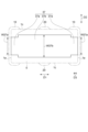
図1~図9を参照して、本実施形態に係る積層貫通コンデンサCD1の構成を説明する。図1は、本実施形態に係る積層貫通コンデンサを示す斜視図である。図2は、素体及び複数の内部電極を示す分解斜視図である。図3及び図4は、本実施形態に係る積層貫通コンデンサの断面構成を示す図である。図5~図9のそれぞれは、内部電極を示す平面図である。 The configuration of the multilayer feedthrough capacitor CD1 according to this embodiment will be described with reference to Figures 1 to 9. Figure 1 is a perspective view showing the multilayer feedthrough capacitor according to this embodiment. Figure 2 is an exploded perspective view showing the element body and multiple internal electrodes. Figures 3 and 4 are diagrams showing the cross-sectional configuration of the multilayer feedthrough capacitor according to this embodiment. Each of Figures 5 to 9 is a plan view showing the internal electrodes.
図1~図4に示されるように、積層貫通コンデンサCD1は、素体1と、一対の外部電極10と、外部電極20と、複数の内部電極30と、を備えている。一対の外部電極10は、互いに離間して素体1上に配置されている。外部電極20は、一対の外部電極10と離間して素体1上に配置されている。複数の内部電極30は、素体1内に配置されている。
As shown in Figures 1 to 4, the multilayer feedthrough capacitor CD1 comprises an
素体1は、直方体形状を呈する。本明細書において、直方体形状は、角部及び稜線部が面取りされている直方体の形状、又は、角部及び稜線部が丸められている直方体の形状を含む。素体1は、互いに対向する一対の端面1aと、一対の端面1aを連結している四つの側面1cを含む。素体1の外表面は、一対の端面1aと四つの側面1cとを含む。一対の端面1a及び四つの側面1cのそれぞれは、矩形状を呈する。本明細書において、矩形状は、たとえば、各角が面取りされている形状、又は、各角が丸められている形状を含む。図1では、複数の内部電極30の図示が省略されている。
The
素体1は、複数の誘電体層5を含む。各誘電体層5は、第三方向D3に積層されている。各誘電体層5は、誘電体材料を含むセラミックグリーンシートの焼結体から構成されている。誘電体材料は、たとえば、BaTiO3系、Ba(Ti,Zr)O3系、又は(Ba,Ca)TiO3系を含む誘電体セラミックを含んでいる。各誘電体層5は、各誘電体層5の間の境界が視認できない程度に一体化されている。
The
一対の端面1aは、第一方向D1で互いに対向する。四つの側面1cのうち、一対の側面1cは、第二方向D2で互いに対向する。別の一対の側面1cは、第三方向D3で互いに対向する。四つの側面1cは、一対の端面1aを連結するように、第一方向D1に延在する。第一方向D1は、第二方向D2に交差すると共に、第三方向D3に交差する。第二方向D2は、第三方向D3に交差する。本実施形態では、第一方向D1、第二方向D2、及び第三方向D3は、互いに直交する。
素体1の第一方向D1での長さは、たとえば、0.8~3.4mmである。素体1の第二方向D2での長さは、たとえば、0.3~1.8mmである。素体1の第三方向D3での長さは、たとえば、0.3~1.8mmである。素体1では、たとえば、第一方向D1が長辺方向である。
A pair of end faces 1a face each other in a first direction D1. Of the four side faces 1c, a pair of side faces 1c face each other in a second direction D2. Another pair of side faces 1c face each other in a third direction D3. The four side faces 1c extend in the first direction D1 so as to connect the pair of end faces 1a. The first direction D1 intersects with the second direction D2 and also intersects with the third direction D3. The second direction D2 intersects with the third direction D3. In this embodiment, the first direction D1, the second direction D2, and the third direction D3 are perpendicular to each other.
The length of the
一対の外部電極10のそれぞれは、一対の端面1aのうち対応する端面1a上と、四つの側面1c上とに配置されている。各外部電極10は、対応する端面1a上に位置する第一電極部分と、四つの側面1cのそれぞれ一部上に位置する第二電極部分とを含む。第一電極部分は、第二電極部分に連続している。第二電極部分は、側面1cにおける、対応する端面1a寄りの領域を覆っている。一対の外部電極10は、信号用外部電極を含む。
Each of the pair of
外部電極20は、一対の側面1c上に配置されている。積層貫通コンデンサCD1は、一対の外部電極20を含んでもよい。図1は、積層貫通コンデンサCD1が一対の外部電極20を含む例を示している。一対の外部電極20のそれぞれは、一対の側面1cのうち対応する側面1c上に配置されている一対の外部電極20は、互いに離間し、第二方向D2で互いに対向している。積層貫通コンデンサCD1は、一つの外部電極20のみを含んでもよい。この場合、上記一つの外部電極20は、たとえば、一対の側面1cのいずれか一方上に配置される。外部電極20は、グラウンド用外部電極を含む。たとえば、外部電極10が第一外部電極を含む場合、外部電極20は、第二外部電極を含む。
The
図3及び図4に示されるように、外部電極10,20は、下地層10a,20aを含む。下地層10a,20aは、終結金属層を含む。焼結金属層は、導電性ペーストを素体1の外表面に付与し、焼き付けることによって形成される。導電性ペーストは、金属粉末、ガラス成分、有機バインダ、及び有機溶剤を含む。導電性ペーストに含まれる金属粉末は、たとえば、Cu粉末又はNi粉末を含む。下地層10a,20aは、導電性ペーストに含まれる金属粉末が焼結した層を含む。外部電極10,20は、下地層10a,20a上に少なくとも一つのめっき層を含む。本実施形態では、外部電極10は、下地層10a上に二つのめっき層10b,10cを含み、外部電極20は、下地層20a上に二つのめっき層20b,20cを含む。下地層10a,20aは、めっき層10b,20bを形成するための下地層である。めっき層10bは、下地層10aとめっき層10cとの間に位置し、めっき層20bは、下地層20aとめっき層20cとの間に位置する。めっき層10b,20bは、たとえば、Niめっき層を含む。めっき層10b,20bは、Niめっき層の代わりに、Snめっき層、Cuめっき層、又はAuめっき層を含んでもよい。めっき層10c,20cは、はんだめっき層を含む。はんだめっき層は、Snめっき層、Sn-Ag合金めっき層、Sn-Bi合金めっき層、又はSn-Cu合金めっき層を含む。これらのめっき層は、めっき法によって形成される。めっき法は、たとえば、電解めっき法を含む。
3 and 4, the
図2~図4に示されるように、素体1は、領域R1、領域R2、及び領域R3を含む。領域R1と領域R3とは、信号用内部電極とグラウンド用内部電極とを含み、主として、積層貫通コンデンサCD1の静電容量の形成に寄与する。領域R2は、通電用内部電極を含み、主として、積層貫通コンデンサCD1の直流抵抗(Rdc)の低減に寄与する。領域R2は、領域R1と領域R3との間に配置されている。本実施形態では、領域R2は、第三方向D3で、領域R1と領域R3との間に配置されている。たとえば、領域R1が第一領域を含む場合、領域R2は、第二領域を含み、領域R3は、第三領域を含む。
As shown in Figures 2 to 4, the
領域R1には、複数の内部電極31と、複数の内部電極33と、が配置されている。すなわち、領域R1には、少なくとも一つの内部電極31と、少なくとも一つの内部電極33と、が配置されている。複数の内部電極30は、内部電極31と内部電極33と、を含む。内部電極31は、信号用内部電極を含む。内部電極33は、グラウンド用内部電極を含む。図2~図4に示されるように、各内部電極31と各内部電極33とは、誘電体層5を挟んで、互いに対向している。各内部電極31と各内部電極33とは、間隔L1で、互いに対向している。各内部電極31と各内部電極33とは、交互に配置されている。たとえば、内部電極31が第一内部電極を含む場合、内部電極33は、第三内部電極を含む。
A plurality of
図5に示されるように、内部電極31は、第一方向D1に延在し、一対の端面1aのそれぞれに露出する。内部電極31は、一対の外部電極10のそれぞれに接続されている。内部電極31は、一対の外部電極10に電気的に接続されている。内部電極31は、側面1cに露出しないで、側面1cから離間している。内部電極31は、外部電極20に接続されていない。
As shown in FIG. 5, the
内部電極31は、接続領域31aと電極領域31bとを含む。内部電極31は、二つの接続領域31aと一つの電極領域31bとを含む。一つの電極領域31bは、第一方向D1で、二つの接続領域31aの間に位置する。二つの接続領域31aと一つの電極領域31bとは、互いに連続している。接続領域31a及び電極領域31bは、第三方向D3から見て、矩形状を呈する。たとえば、接続領域31aが第一接続領域を含む場合、電極領域31bは、第一電極領域を含む。
The
二つの接続領域31aのそれぞれは、一対の外部電極10のうち対応する外部電極10に接続されている。接続領域31aのそれぞれと、上記対応する外部電極10とが互いに接続する、接続領域31aのそれぞれは、接続幅W31aで、上記対応する外部電極10と接続されている。接続幅W31aは、少なくとも一つの内部電極31における、一対の外部電極10のそれぞれとの接続端の長さである。接続幅W31aは、たとえば、接続領域31aの第二方向D2での幅と同一である。電極領域31bは、第二方向D2に幅W31bを有する。接続幅W31aは、たとえば、幅W31bより小さい。接続幅W31aは、幅W31b以下であってもよい。接続幅W31aは、幅W31bと同一であってもよい。接続領域31aの第二方向D2での幅は、電極領域31bの第二方向D2での幅と同一であってもよい。図2及び図5は、接続幅W31aが幅W31bより小さい例を示している。少なくとも一つの内部電極31は、接続幅W31aが異なる複数の内部電極31を含む。複数の内部電極31のそれぞれは、たとえば、互いに異なる接続幅W31aを有する。
本明細書において、幅が「同一」であるとは、幅の大きさが互いに等しい場合に加えて、予め設定した範囲での微差又は製造誤差などを含んだ幅の大きさが互いに等しい場合を含んでよい。たとえば、接続幅W31aの平均値が、幅W31bの平均値の±10%の範囲内に収まる場合、接続幅W31aは、幅W31bと同一であるとされる。
Each of the two
In this specification, the term "same width" may include the case where the widths are equal to each other, as well as the case where the widths are equal to each other including slight differences or manufacturing errors within a preset range. For example, when the average value of the connection width W31a falls within a range of ±10% of the average value of the width W31b, the connection width W31a is considered to be the same as the width W31b.
図6に示されるように、内部電極33は、第二方向D2に延在し、一対の側面1cの少なくとも一つに露出する。内部電極33は、外部電極20に接続されている。内部電極33は、一対の側面1cのそれぞれに露出し、外部電極20のそれぞれに接続されている。内部電極33は、外部電極20に電気的に接続されている。内部電極33は、端面1aに露出しないで、端面1aから離間している。内部電極33は、外部電極10に接続されていない。少なくとも一つの内部電極33は、電極領域31bと対向している。
As shown in FIG. 6, the
内部電極33は、接続領域33aと電極領域33bとを含む。内部電極33は、二つの接続領域33aと一つの電極領域33bとを含む。一つの電極領域33bは、第二方向D2で、二つの接続領域33aの間に位置する。二つの接続領域33aと一つの電極領域33bとは、互いに連続している。接続領域33a及び電極領域33bは、第三方向D3から見て、矩形状を呈する。たとえば、接続領域33aが第三接続領域を含む場合、電極領域33bは、第三電極領域を含む。
The
二つの接続領域33aのそれぞれは、一対の外部電極20のうち対応する外部電極20に接続されている。接続領域33aは、上記対応する外部電極20と電気的に接続されている。接続領域33aの第一方向D1での幅は、電極領域33bの第一方向D1での幅より小さい。電極領域33bは、第二方向D2に幅W33bを有する。幅W33bは、たとえば、幅W31bと同一である。幅W33bは、たとえば、幅W31bと同一である。幅W33bは、接続幅W31aより大きくてもよい。幅W33bは、接続幅W31a以上でもよい。
Each of the two
領域R2には、複数の内部電極32が配置されている。すなわち、領域R2には、少なくとも一つの内部電極32が配置されている。複数の内部電極30は、内部電極32を含む。領域R2では、少なくとも一つの内部電極32が配置されている。少なくとも一つの内部電極32は、複数の内部電極32を含む。内部電極32は、通電用内部電極を含む。図2~図4に示されるように、複数の内部電極32は、誘電体層5を挟んで、互いに対向している。複数の内部電極32は、間隔L2で、互いに対向している。各内部電極34と各内部電極35とは、交互に配置されている。間隔L2は、たとえば、間隔L1より小さい。したがって、少なくとも一つの内部電極32は、少なくとも一つの内部電極31と少なくとも一つの内部電極33との間隔L1より小さい間隔L2で対向している。複数の内部電極32は、内部電極33と対向する内部電極32を含んでもよい。この場合、複数の内部電極32は、内部電極33と対向しない内部電極32を必ず含むことが必要である。たとえば、内部電極31が第一内部電極を含む場合、内部電極32は、第二内部電極を含む。
A plurality of
図7に示されるように、内部電極32は、第一方向D1に延在し、一対の端面1aのそれぞれに露出する。内部電極32は、一対の外部電極10のそれぞれに接続されている。内部電極32は、一対の外部電極10に電気的に接続されている。内部電極32は、側面1cに露出しないで、側面1cから離間している。内部電極32は、外部電極20に接続されていない。内部電極32は、第三方向D3から見て、矩形状を呈する。
As shown in FIG. 7, the
内部電極32は、接続幅W32aで、一対の外部電極10と接続されている。接続幅W32aは、少なくとも一つの内部電極32における、一対の外部電極10のそれぞれとの接続端の長さである。内部電極32は、第二方向D2に幅W32bを有する。接続幅W32aは、たとえば、幅W32bと同一である。幅W32bは、たとえば、幅W31bと同一である。幅W32bは、幅W31bより大きくてもよい。たとえば、接続幅W31aが第一接続幅を含む場合、接続幅W32aは、第二接続幅を含む。
The
本実施形態では、幅W32bは、接続幅W32a、幅W31b、及び幅W33bの全てと同一であり、かつ、接続幅W31aより大きい。幅W32bは、接続幅W32aと同一であり、かつ、幅W31b及び幅W33bより大きいと共に、幅W31b及び幅W33bは、接続幅W31a以上であってもよい。 In this embodiment, the width W32b is the same as all of the connection width W32a, the width W31b, and the width W33b, and is larger than the connection width W31a. The width W32b is the same as the connection width W32a, and is larger than the width W31b and the width W33b, and the width W31b and the width W33b may be equal to or larger than the connection width W31a.
領域R3には、複数の内部電極34と、複数の内部電極35と、が配置されている。すなわち、領域R3には、少なくとも一つの内部電極34と、少なくとも一つの内部電極35と、が配置されている。複数の内部電極30は、内部電極34と内部電極35と、を含む。内部電極34は、信号用内部電極を含む。内部電極35は、グラウンド用内部電極を含む。図2~図4に示されるように、各内部電極34と各内部電極35とは、誘電体層5を挟んで、互いに対向している。各内部電極34と各内部電極35とは、間隔L3で、互いに対向している。各内部電極34と各内部電極35とは、交互に配置されている。間隔L2は、たとえば、間隔L3より小さい。したがって、少なくとも一つの内部電極32は、少なくとも一つの内部電極34と少なくとも一つの内部電極35との間隔L3より小さい間隔L2で対向している。複数の内部電極32は、内部電極35と対向する内部電極32を含んでもよい。この場合、複数の内部電極32は、内部電極35と対向しない内部電極32を必ず含むことが必要である。たとえば、内部電極31が第一内部電極を含む場合、内部電極34は、第四内部電極を含み、内部電極35は、第五内部電極を含む。
In region R3, a plurality of
図8に示されるように、内部電極34は、第一方向D1に延在し、一対の端面1aのそれぞれに露出する。内部電極34は、一対の外部電極10のそれぞれに接続されている。内部電極34は、一対の外部電極10に電気的に接続されている。内部電極34は、側面1cに露出しないで、側面1cから離間している。内部電極34は、外部電極20に接続されていない。
As shown in FIG. 8, the
内部電極34は、接続領域34aと電極領域34bとを含む。内部電極34は、二つの接続領域34aと一つの電極領域34bとを含む。一つの電極領域34bは、第一方向D1で、二つの接続領域34aの間に位置する。二つの接続領域34aと一つの電極領域34bとは、互いに連続している。接続領域34a及び電極領域34bは、第三方向D3から見て、矩形状を呈する。たとえば、接続領域34aが第四接続領域を含む場合、電極領域34bは、第四電極領域を含む。
The
二つの接続領域34aのそれぞれは、一対の外部電極10のうち対応する外部電極10に接続されている。接続領域34aのそれぞれと、上記対応する外部電極10とが互いに接続する、接続領域34aのそれぞれは、接続幅W34aで、上記対応する外部電極10と接続されている。接続幅W34aは、少なくとも一つの内部電極34における、一対の外部電極10のそれぞれとの接続端の長さである。接続幅W34aは、たとえば、接続領域34aの第二方向D2での幅と同一である。電極領域34bは、第二方向D2に幅W34bを有する。接続幅W34aは、たとえば、幅W34bより小さい。接続幅W34aは、幅W34b以下であってもよい。接続幅W34aは、幅W34bと同一であってもよい。接続領域34aの第二方向D2での幅は、電極領域34bの第二方向D2での幅と同一であってもよい。図2及び図8は、接続幅W34aが幅W34bより小さい例を示している。たとえば、接続幅W31aが第一接続幅を含む場合、接続幅W34aは、第三接続幅を含む。
Each of the two
図9に示されるように、内部電極35は、第二方向D2に延在し、一対の側面1cの少なくとも一つに露出する。内部電極35は、外部電極20に接続されている。内部電極35は、一対の側面1cのそれぞれに露出し、外部電極20のそれぞれに接続されている。内部電極35は、外部電極20に電気的に接続されている。内部電極35は、端面1aに露出しないで、端面1aから離間している。内部電極35は、外部電極10に接続されていない。少なくとも一つの内部電極35は、電極領域34bと対向している。
9, the
内部電極35は、接続領域35aと電極領域35bとを含む。内部電極35は、二つの接続領域35aと一つの電極領域35bとを含む。一つの電極領域35bは、第二方向D2で、二つの接続領域35aの間に位置する。二つの接続領域35aと一つの電極領域35bとは、互いに連続している。接続領域35a及び電極領域35bは、第三方向D3から見て、矩形状を呈する。たとえば、接続領域35aが第五接続領域を含む場合、電極領域35bは、第五電極領域を含む。
The
二つの接続領域35aのそれぞれは、一対の外部電極20のうち対応する外部電極20に接続されている。接続領域35aは、上記対応する外部電極20と電気的に接続されている。接続領域35aの第一方向D1での幅は、電極領域35bの第一方向D1での幅より小さい。
Each of the two
電極領域35bは、第二方向D2に幅W35bを有する。幅W35bは、たとえば、幅W31bと同一である。幅W35bは、たとえば、幅W31bと同一である。幅W35bは、接続幅W31aより大きくてもよい。幅W35bは、接続幅W31a以上でもよい。幅W35bは、たとえば、幅W34bと同一である。幅W35bは、接続幅W34aより大きくてもよい。幅W35bは、接続幅W34a以上でもよい。
The
二つの接続領域35aのそれぞれは、一対の外部電極20のうち対応する外部電極20に接続されている。接続領域35aは、上記対応する外部電極20と電気的に接続されている。接続領域35aの第一方向D1での幅は、電極領域35bの第一方向D1での幅より小さい。
Each of the two
複数の内部電極30は、積層型の電気素子の内部電極として通常用いられる導電性材料を含む。複数の内部電極30に含まれる導電性材料は、Ni又はCuを含む。複数の内部電極30は、上記導電性材料を含む導電性ペーストの焼結体として構成される。
The multiple
図3及び図4で示した例では、領域R1は、二つの内部電極31と二つの内部電極33とを含み、領域R1が含む内部電極の総数は、四つである。領域R2は、四つの内部電極32を含み、領域R2が含む内部電極の総数は、四つである。領域R2が含む内部電極の総数は、領域R1が含む内部電極の総数と同一である。本実施形態では、領域R2が含む内部電極の総数が、領域R1が含む内部電極の総数と同一である場合に限られない。すなわち、領域R2が含む誘電体層5の層数が、領域R1が含む誘電体層5の層数と同一である場合に限られない。
3 and 4, region R1 includes two
上述したように、間隔L2は、たとえば、間隔L1より小さい。間隔L2が間隔L1より小さい場合、領域R2が含む各誘電体層5の厚みは、領域R1が含む各誘電体層5の厚みより小さい。領域R2が含む各誘電体層5の厚みは、たとえば、領域R1が含む各誘電体層5の厚みの約1/10~1/2である。したがって、領域R2が含む各誘電体層5の層数は、領域R1が含む各誘電体層5の層数より多くてもよい。すなわち、領域R2が含む内部電極の総数は、領域R1が含む内部電極の総数より多くてもよい。
本実施形態では、領域R2が含む各誘電体層5の層数は、10~500層であってもよい。領域R1が含む各誘電体層5の層数は、3~300層であってもよい。
As described above, the interval L2 is, for example, smaller than the interval L1. When the interval L2 is smaller than the interval L1, the thickness of each
In this embodiment, the number of the
図3及び図4で示した例では、領域R3は、二つの内部電極34と二つの内部電極35とを含み、領域R3が含む内部電極の総数は、四つである。領域R2が含む内部電極の総数は、領域R3が含む内部電極の総数と同一である。本実施形態では、領域R2が含む内部電極の総数が、領域R3が含む内部電極の総数と同一である場合に限られない。すなわち、領域R2が含む誘電体層5の層数が、領域R3が含む誘電体層5の層数と同一である場合に限られない。
3 and 4, region R3 includes two
上述したように、間隔L2は、たとえば、間隔L3より小さい。間隔L2が間隔L3より小さい場合、領域R2に含まれる各誘電体層5の厚みは、領域R3に含まれる各誘電体層5の厚みより小さい。領域R2に含まれる各誘電体層5の厚みは、たとえば、領域R3に含まれる各誘電体層5の厚みの約1/10~1/2である。したがって、領域R2が含む各誘電体層5の層数は、領域R3が含む各誘電体層5の層数より多くてもよい。すなわち、領域R2が含む内部電極の総数は、領域R3が含む内部電極の総数より多くてもよい。
本実施形態では、領域R3が含む各誘電体層5の層数は、3~300層であってもよい。
As described above, the interval L2 is, for example, smaller than the interval L3. When the interval L2 is smaller than the interval L3, the thickness of each
In this embodiment, the number of
積層貫通コンデンサCD1は、電子機器に実装される。上記電子機器は、回路基板又は電子部品を含む。たとえば、積層貫通コンデンサCD1は、上記電子機器に、はんだ実装される。積層貫通コンデンサCD1では、側面1cのいずれかが、上記電子機器に対向する実装面を含む。 The multilayer feedthrough capacitor CD1 is mounted on an electronic device. The electronic device includes a circuit board or electronic components. For example, the multilayer feedthrough capacitor CD1 is solder mounted on the electronic device. In the multilayer feedthrough capacitor CD1, one of the side surfaces 1c includes a mounting surface that faces the electronic device.
図10及び図11を参照して、本実施形態の第一変形例に係る積層貫通コンデンサCD2について説明する。図10は、素体及び複数の内部電極を示す分解斜視図である。図11は、内部電極を示す平面図である。積層貫通コンデンサCD2は、概ね、上述した積層貫通コンデンサCD1と類似又は同じであるが、積層貫通コンデンサCD2は、素体1及び複数の内部電極30の構成に関して、積層貫通コンデンサCD1と相違する。以下、積層貫通コンデンサCD1と積層貫通コンデンサCD2との相違点を主として説明する。
With reference to Figures 10 and 11, a multilayer feedthrough capacitor CD2 according to a first modified example of this embodiment will be described. Figure 10 is an exploded perspective view showing the element body and multiple internal electrodes. Figure 11 is a plan view showing the internal electrodes. The multilayer feedthrough capacitor CD2 is generally similar to or the same as the multilayer feedthrough capacitor CD1 described above, but the multilayer feedthrough capacitor CD2 differs from the multilayer feedthrough capacitor CD1 in terms of the configuration of the
図10に示されるように、第一変形例では、素体1は、領域R1、領域R2、及び領域R4を含む。領域R1は、領域R2と領域R4との間に位置する。本実施形態では、領域R1は、第三方向D3で、領域R2と領域R4との間に位置する。たとえば、領域R1が第一領域を含む場合、領域R4は、第四領域を含む。
As shown in FIG. 10, in the first modified example, the
領域R4には、複数の内部電極36が配置されている。すなわち、領域R4には、少なくとも一つの内部電極36が配置されている。複数の内部電極30は、内部電極36を含む。領域R4では、少なくとも一つの内部電極36が配置されている。内部電極36は、通電用内部電極を含む。たとえば、内部電極31が第一内部電極を含む場合、内部電極36は、第六内部電極を含む。
A plurality of
図11に示されるように、内部電極36は、第一方向D1に延在し、一対の端面1aのそれぞれに露出する。内部電極36は、一対の外部電極10のそれぞれに接続されている。内部電極36は、一対の外部電極10に電気的に接続されている。内部電極36は、側面1cに露出しないで、側面1cから離間している。内部電極36は、外部電極20に接続されていない。内部電極36は、第三方向D3から見て、矩形状を呈する。
内部電極36は、接続幅W36aで、一対の外部電極10と接続されている。接続幅W36aは、少なくとも一つの内部電極36における、一対の外部電極10のそれぞれとの接続端の長さである。内部電極36は、第二方向D2に幅W36bを有する。接続幅W36aは、たとえば、幅W36bと同一である。幅W36bは、たとえば、幅W31bと同一である。幅W36bは、幅W31bより大きくてもよい。たとえば、接続幅W31aが第一接続幅を含む場合、接続幅W36aは、第四接続幅を含む。
11 , the
The
図12を参照して、本実施形態の第二変形例に係る積層貫通コンデンサCD3について説明する。図12は、素体及び複数の内部電極を示す分解斜視図である。積層貫通コンデンサCD3は、概ね、上述した積層貫通コンデンサCD1と類似又は同じであるが、積層貫通コンデンサCD3は、素体1及び複数の内部電極30の構成に関して、積層貫通コンデンサCD1と相違する。以下、積層貫通コンデンサCD1と積層貫通コンデンサCD3との相違点を主として説明する。
With reference to FIG. 12, a multilayer feedthrough capacitor CD3 according to a second modified example of this embodiment will be described. FIG. 12 is an exploded perspective view showing the element body and multiple internal electrodes. The multilayer feedthrough capacitor CD3 is generally similar to or the same as the multilayer feedthrough capacitor CD1 described above, but the multilayer feedthrough capacitor CD3 differs from the multilayer feedthrough capacitor CD1 in terms of the configuration of the
第二変形例では、素体1は、領域R1、領域R2、領域R3、領域R4、及び領域R5を含む。領域R5には、複数の内部電極31と、複数の内部電極33と、が配置されている。すなわち、領域R5には、少なくとも一つの内部電極31と、少なくとも一つの内部電極33と、が配置されている。各内部電極31と各内部電極33とは、誘電体層5を挟んで、互いに対向している。各内部電極31と各内部電極33とは、交互に配置されている。第二変形例では、領域R1、領域R2、領域R3、領域R4、及び領域R5は、第三方向D3で、領域R1、領域R2、領域R3、領域R4、及び領域R5の順に配置されている。第二変形例では、接続幅W31aが幅W31bより小さく、接続幅W34aが幅W34bより小さい。
In the second modified example, the
図13~図15を参照して、本実施形態の第三変形例に係る積層貫通コンデンサCD4について説明する。図13は、素体及び複数の内部電極を示す分解斜視図である。図14及び図15は、各内部電極を示す平面図である。積層貫通コンデンサCD4は、概ね、上述した積層貫通コンデンサCD1と類似又は同じであるが、積層貫通コンデンサCD4は、素体1及び複数の内部電極30の構成に関して、積層貫通コンデンサCD1と相違する。以下、積層貫通コンデンサCD1と積層貫通コンデンサCD4との相違点を主として説明する。
With reference to Figures 13 to 15, a multilayer feedthrough capacitor CD4 according to a third modified example of this embodiment will be described. Figure 13 is an exploded perspective view showing the element body and multiple internal electrodes. Figures 14 and 15 are plan views showing the internal electrodes. The multilayer feedthrough capacitor CD4 is generally similar to or the same as the multilayer feedthrough capacitor CD1 described above, but the multilayer feedthrough capacitor CD4 differs from the multilayer feedthrough capacitor CD1 in terms of the configuration of the
第三変形例では、素体1は、領域R2、領域R6、及び領域R7を含む。領域R2、領域R6、及び領域R7は、第三方向D3で、領域R6、領域R2、及び領域R7の順に配置されている。領域R2は、少なくとも一つの内部電極32を含む。領域R2では、少なくとも一つの内部電極32が配置されている。
領域R6には、複数の内部電極31と、複数の内部電極33と、複数の内部電極37と、複数の内部電極38と、が配置されている。すなわち、領域R6には、少なくとも一つの内部電極31と、少なくとも一つの内部電極33と、少なくとも一つの内部電極37と、少なくとも一つの内部電極38と、が配置されている。複数の内部電極30は、内部電極31,33,37,38を含む。内部電極37,38は、信号用内部電極を含む。各内部電極37,38と各内部電極33とは、誘電体層5を挟んで、互いに対向している。各内部電極37,38と各内部電極33とは、交互に配置されている。領域R6では、内部電極37は、内部電極31よりも領域R2の近くに配置され、内部電極38は、内部電極37よりも領域R2の近くに配置されている。
In the third modified example, the
In the region R6, a plurality of
図14に示されるように、内部電極37は、一対の外部電極10のそれぞれに接続されている。内部電極37は、二つの接続領域37aと一つの電極領域37bとを含む。一つの電極領域37bは、第一方向D1で、二つの接続領域37aの間に位置する。接続領域37a及び電極領域37bは、第三方向D3から見て、矩形状を呈する。
As shown in FIG. 14, the
二つの接続領域37aのそれぞれは、一対の外部電極10のうち対応する外部電極10に接続されている。接続領域37aのそれぞれは、接続幅W37aで、上記対応する外部電極10と接続されている。接続幅W37aは、たとえば、接続領域37aの第二方向D2での幅と同一である。接続幅W37aは、接続幅W31aより大きく、幅W37bより小さい。幅W37bは、たとえば、幅W31bと同一である。
Each of the two
図15に示されるように、内部電極38は、一対の外部電極10のそれぞれに接続されている。内部電極38は、接続幅W38aで、一対の外部電極10と接続されている。内部電極38は、第二方向D2に幅W38bを有する。接続幅W38aは、たとえば、幅W38bと同一である。接続幅W38aは、接続幅W37aより大きい。幅W38bは、たとえば、幅W31bと同一である。
As shown in FIG. 15, the
領域R7には、複数の内部電極31と、複数の内部電極33と、複数の内部電極37と、複数の内部電極38と、が配置されている。すなわち、領域R7には、少なくとも一つの内部電極31と、少なくとも一つの内部電極33と、少なくとも一つの内部電極37と、少なくとも一つの内部電極38と、が配置されている。各内部電極37,38と各内部電極33とは、誘電体層5を挟んで、互いに対向している。各内部電極37,38と各内部電極33とは、交互に配置されている。領域R7では、内部電極37は、内部電極31よりも領域R2の近くに配置され、内部電極38は、内部電極37よりも領域R2の近くに配置されている。
In region R7, multiple
以上説明したように、積層貫通コンデンサCD1,CD2,CD3,CD4では、少なくとも一つの内部電極32が、少なくとも一つの内部電極31とは別に、一対の外部電極10に接続されている。少なくとも一つの内部電極32は、少なくとも一つの内部電極31と少なくとも一つの内部電極33とが対向して配置されている領域R1とは別の、領域R2に配置されている。したがって、少なくとも一つの内部電極32は、直流抵抗の低減に寄与する。
積層貫通コンデンサCD1,CD2,CD3,CD4では、接続幅W31aが接続幅W32aより小さい。すなわち、外部電極10のそれぞれと少なくとも一つの内部電極32との接続長さは、外部電極10のそれぞれと少なくとも一つの内部電極31との接続長さより大きい。したがって、電流が、少なくとも一つの内部電極32に流れやすい。少なくとも一つの内部電極32は、直流抵抗の低減により一層寄与する。
これらの結果、積層貫通コンデンサCD1,CD2,CD3,CD4は、直流抵抗を低減する。
積層貫通コンデンサCD1,CD2,CD3,CD4では、接続幅W31aが接続幅W32aより小さい。すなわち、少なくとも一つの内部電極31における、一対の外部電極10のそれぞれとの接続端の長さは、少なくとも一つの内部電極32における、一対の外部電極10のそれぞれとの接続端の長さより小さい。したがって、めっき液は、少なくとも一つの内部電極31の上記接続端と素体1との界面から、素体1内に浸入しがたい。この結果、積層貫通コンデンサCD1,CD2,CD3,CD4は、信頼性の低下を抑制する。
As described above, in the multilayer feedthrough capacitors CD1, CD2, CD3, and CD4, at least one
In the multilayer feedthrough capacitors CD1, CD2, CD3, and CD4, the connection width W31a is smaller than the connection width W32a. That is, the connection length between each of the
As a result, the feedthrough multilayer capacitors CD1, CD2, CD3, and CD4 reduce the DC resistance.
In the multilayer feedthrough capacitors CD1, CD2, CD3, and CD4, the connection width W31a is smaller than the connection width W32a. That is, the length of the connection end of at least one
積層貫通コンデンサCD1では、複数の内部電極30は、一対の外部電極10に接続されている少なくとも一つの内部電極34と、外部電極20に接続されている少なくとも一つの内部電極35と、を含む。素体1は、少なくとも一つの内部電極34と少なくとも一つの内部電極35とが対向して配置されている領域R3を含む。一対の外部電極10のそれぞれと少なくとも一つの内部電極34との接続幅W34aは、接続幅W32aより小さい。領域R2は、領域R1と領域R3との間に位置している。
積層貫通コンデンサCD1では、外部電極10のそれぞれと少なくとも一つの内部電極32との接続長さは、外部電極10のそれぞれと少なくとも一つの内部電極34との接続長さより大きい。したがって、電流が、少なくとも一つの内部電極32に流れやすい。少なくとも一つの内部電極32は、直流抵抗の低減により一層寄与する。この結果、積層貫通コンデンサCD1は、直流抵抗をより一層低減する。
積層貫通コンデンサCD1では、少なくとも一つの内部電極34における、一対の外部電極10のそれぞれとの接続端の長さは、少なくとも一つの内部電極32における、一対の外部電極10のそれぞれとの接続端の長さより小さい。したがって、めっき液は、少なくとも一つの内部電極34の上記接続端と素体1との界面から、素体1内に浸入しがたい。この結果、積層貫通コンデンサCD1は、信頼性の低下を抑制する。
積層貫通コンデンサCD1では、領域R1と領域R3とは、領域R2に比して、稜部に近付く傾向がある。すなわち、領域R1と領域R3とは、領域R2に比して、めっき液が侵入しやすいおそれがある。しかしながら、積層貫通コンデンサCD1では、接続幅W31aが接続幅W32aより小さく、かつ、接続幅W34aが接続幅W32aより小さく、上述したように、めっき液が素体1内に浸入しがたい。したがって、領域R2が、領域R1と領域R3との間に位置する構成においても、信頼性の低下の抑制が維持され得る。
In the multilayer feedthrough capacitor CD1, the multiple
In the multilayer feedthrough capacitor CD1, the connection length between each of the
In the multilayer feedthrough capacitor CD1, the length of the connection end of at least one
In the multilayer feedthrough capacitor CD1, regions R1 and R3 tend to be closer to the ridge than region R2. That is, there is a risk that plating solution may more easily penetrate into regions R1 and R3 than into region R2. However, in the multilayer feedthrough capacitor CD1, the connection width W31a is smaller than the connection width W32a, and the connection width W34a is also smaller than the connection width W32a, so that, as described above, plating solution is less likely to penetrate into the
積層貫通コンデンサCD1では、少なくとも一つの内部電極34は、少なくとも一つの内部電極35と対向すると共に接続幅W34aより大きい幅を有する電極領域34bを含む。
積層貫通コンデンサCD1は、少なくとも一つの内部電極34と少なくとも一つの内部電極35との対向面積を増加させる傾向がある。したがって、積層貫通コンデンサCD1は、静電容量を増加させ得る。
In the multilayer feedthrough capacitor CD1, at least one
The multilayer feedthrough capacitor CD1 tends to increase the opposing area between at least one
積層貫通コンデンサCD1では、少なくとも一つの内部電極32は、間隔L3より小さい間隔L2で対向する複数の内部電極32を含む。
積層貫通コンデンサCD1は、領域R2に配置される内部電極32の数を増加させ得る。したがって、積層貫通コンデンサCD1は、直流抵抗をより一層低減し得る。
積層貫通コンデンサCD1は、少なくとも一つの内部電極34と少なくとも一つの内部電極35との間隔を増加させ得る。したがって、積層貫通コンデンサCD1は、少なくとも一つの内部電極34と少なくとも一つの内部電極35との短絡を抑制する。
In the multilayer feedthrough capacitor CD1, at least one
The multilayer feedthrough capacitor CD1 can increase the number of
The multilayer feedthrough capacitor CD1 can increase the distance between the at least one
積層貫通コンデンサCD1では、内部電極31は、内部電極33と対向すると共に接続幅W31aより大きい幅を有する電極領域31bを含む。
積層貫通コンデンサCD1では、少なくとも一つの内部電極31と少なくとも一つの内部電極33との対向面積を増加させる傾向がある。したがって、積層貫通コンデンサCD1は、静電容量を増加させ得る。
In the multilayer feedthrough capacitor CD1, the
In the multilayer feedthrough capacitor CD1, there is a tendency to increase the opposing area between at least one
積層貫通コンデンサCD1では、少なくとも一つの内部電極32は、間隔L1より小さい間隔L2で対向する複数の内部電極32を含む。
積層貫通コンデンサCD1は、領域R2に配置される内部電極32の数を増加させ得る。したがって、積層貫通コンデンサCD1は、直流抵抗をより一層低減し得る。
積層貫通コンデンサCD1は、少なくとも一つの内部電極31と少なくとも一つの内部電極33との間隔を増加させ得る。したがって、積層貫通コンデンサCD1は、少なくとも一つの内部電極31と少なくとも一つの内部電極33との短絡を抑制する。
In the multilayer feedthrough capacitor CD1, at least one
The multilayer feedthrough capacitor CD1 can increase the number of
The multilayer feedthrough capacitor CD1 can increase the distance between the at least one
積層貫通コンデンサCD2では、複数の内部電極30は、一対の外部電極10に接続されている少なくとも一つの内部電極36を含む。素体1は、少なくとも一つの内部電極36が配置されている領域R4を含む。接続幅W31aは、一対の外部電極10のそれぞれと少なくとも一つの内部電極36との接続幅W36aより小さい。領域R1は、領域R2と領域R4との間に位置している。
積層貫通コンデンサCD2では、少なくとも一つの内部電極36が、少なくとも一つの内部電極31とは別に、一対の外部電極10に接続されている。少なくとも一つの内部電極36は、少なくとも一つの内部電極31と少なくとも一つの内部電極33とが対向して配置されている領域R1とは別の、領域R4に配置されている。したがって、少なくとも一つの内部電極36は、直流抵抗の低減に寄与する。積層貫通コンデンサCD2では、接続幅W31aが接続幅W36aより小さく、外部電極10のそれぞれと少なくとも一つの内部電極36との接続長さは、外部電極10のそれぞれと少なくとも一つの内部電極31との接続長さより大きい。したがって、電流が、少なくとも一つの内部電極36に流れやすい。少なくとも一つの内部電極36は、直流抵抗の低減により一層寄与する。これらの結果、積層貫通コンデンサCD2は、直流抵抗をより一層低減する。
積層貫通コンデンサCD2では、少なくとも一つの内部電極31における、一対の外部電極10のそれぞれとの接続端の長さは、少なくとも一つの内部電極36における、一対の外部電極10のそれぞれとの接続端の長さより小さい。したがって、めっき液は、少なくとも一つの内部電極31の上記接続端と素体1との界面から、素体1内に浸入しがたい。この結果、積層貫通コンデンサCD2は、信頼性の低下を抑制する。
In the multilayer feedthrough capacitor CD2, the multiple
In the multilayer feedthrough capacitor CD2, at least one
In the multilayer feedthrough capacitor CD2, the length of the connection end of at least one
積層貫通コンデンサCD1では、少なくとも一つの内部電極31は、接続幅W31aが異なる複数の内部電極31を含む。
積層貫通コンデンサCD1でも、複数の内部電極31のそれぞれの接続幅W31aは、接続幅W32aより小さい。したがって、めっき液は、複数の内部電極31のそれぞれの上記接続端と素体1との界面から、素体1内に浸入しがたい。この結果、積層貫通コンデンサCD1は、依然として、信頼性の低下を抑制する。
In the multilayer feedthrough capacitor CD1, at least one
In the multilayer feedthrough capacitor CD1 as well, the connection width W31a of each of the plurality of
以上、本発明の実施形態及び変形例について説明してきたが、本発明は必ずしも上述した実施形態及び変形例に限定されるものではなく、その要旨を逸脱しない範囲で様々な変更が可能である。 Although the embodiments and variations of the present invention have been described above, the present invention is not necessarily limited to the above-mentioned embodiments and variations, and various modifications are possible without departing from the spirit of the present invention.
少なくとも一つの内部電極31,34は、少なくとも一つの内部電極33,35と対向すると共に接続幅W34aより大きい幅を有する電極領域31b,34bを含まなくてもよい。少なくとも一つの内部電極31,34が、少なくとも一つの内部電極33,35と対向すると共に接続幅W31a,W34aより大きい幅を有する電極領域31b,34bを含む構成は、上述したとおり、少なくとも一つの内部電極34と少なくとも一つの内部電極35との対向面積を増加させる傾向がある。したがって、積層貫通コンデンサCD1は、静電容量を増加させ得る。
少なくとも一つの内部電極32は、間隔L1,L3より小さい間隔L2で対向する複数の内部電極32を含まなくてもよい。少なくとも一つの内部電極32が、間隔L2で対向する複数の内部電極32を含む構成は、領域R2に配置される内部電極32の数を増加させ得る。したがって、積層貫通コンデンサCD1は、直流抵抗をより一層低減し得る。少なくとも一つの内部電極31,34と少なくとも一つの内部電極33,35との間隔を増加させ得る。したがって、積層貫通コンデンサCD1は、少なくとも一つの内部電極31,34と少なくとも一つの内部電極33,35との短絡を抑制する。
At least one
The at least one
上述した実施形態及び変形例の記載から把握されるとおり、本明細書は、以下に示す態様の開示を含んでいる。
(付記1)
素体と、
互いに離間して前記素体上に配置されている一対の第一外部電極と、
前記一対の第一外部電極と離間して前記素体上に配置されている第二外部電極と、
前記素体内に配置されている複数の内部電極と、
を備え、
前記複数の内部電極は、前記一対の第一外部電極に接続されている少なくとも一つの第一内部電極と、前記一対の第一外部電極に接続されている少なくとも一つの第二内部電極と、前記第二外部電極に接続されている少なくとも一つの第三内部電極と、を含み、
前記素体は、
前記少なくとも一つの第一内部電極と前記少なくとも一つの第三内部電極とが対向して配置されている第一領域と、
前記少なくとも一つの第二内部電極が配置されている第二領域と、を含み、
前記一対の第一外部電極のそれぞれと前記少なくとも一つの第一内部電極との第一接続幅は、前記一対の第一外部電極のそれぞれと前記少なくとも一つの第二内部電極との第二接続幅より小さい、積層貫通コンデンサ。
(付記2)
前記複数の内部電極は、前記一対の第一外部電極に接続されている少なくとも一つの第四内部電極と、前記第二外部電極に接続されている少なくとも一つの第五内部電極と、を更に含み、
前記素体は、前記少なくとも一つの第四内部電極と前記少なくとも一つの第五内部電極とが対向して配置されている第三領域を更に含み、
前記一対の第一外部電極のそれぞれと前記少なくとも一つの第四内部電極との第三接続幅は、前記第二接続幅より小さく、
前記第二領域は、前記第一領域と前記第三領域との間に位置する、付記1に記載の積層貫通コンデンサ。
(付記3)
前記少なくとも一つの第四内部電極は、前記少なくとも一つの第五内部電極と対向すると共に前記第三接続幅より大きい幅を有する電極領域を含む、付記2に記載の積層貫通コンデンサ。
(付記4)
前記少なくとも一つの第二内部電極は、前記少なくとも一つの第四内部電極と前記少なくとも一つの第五内部電極との間隔より小さい間隔で対向する複数の第二内部電極を含む、付記2又は3に記載の積層貫通コンデンサ。
(付記5)
前記少なくとも一つの第一内部電極は、前記少なくとも一つの第三内部電極と対向すると共に前記第一接続幅より大きい幅を有する電極領域を含む、付記1~4のいずれか一つに記載の積層貫通コンデンサ。
(付記6)
前記少なくとも一つの第二内部電極は、前記少なくとも一つの第一内部電極と前記少なくとも一つの第三内部電極との間隔より小さい間隔で対向する複数の第二内部電極を含む、付記1~5のいずれか一つに記載の積層貫通コンデンサ。
(付記7)
前記複数の内部電極は、前記一対の第一外部電極に接続されている少なくとも一つの第六内部電極を更に含み、
前記素体は、前記少なくとも一つの第六内部電極が配置されている第四領域を更に含み、
前記第一接続幅は、前記一対の第一外部電極のそれぞれと前記少なくとも一つの第六内部電極との第四接続幅より小さく、
前記第一領域は、前記第二領域と前記第四領域との間に位置する、付記1~6のいずれか一つに記載の積層貫通コンデンサ。
(付記8)
前記少なくとも一つの第一内部電極は、前記第一接続幅が異なる複数の第一内部電極を含む、付記1~7のいずれか一つに記載の積層貫通コンデンサ。
As will be understood from the above description of the embodiments and modifications, this specification includes disclosure of the following aspects.
(Appendix 1)
The body and
A pair of first external electrodes disposed on the element body and spaced apart from each other;
a second external electrode disposed on the element body and spaced apart from the pair of first external electrodes;
A plurality of internal electrodes disposed within the element body;
Equipped with
the plurality of internal electrodes include at least one first internal electrode connected to the pair of first external electrodes, at least one second internal electrode connected to the pair of first external electrodes, and at least one third internal electrode connected to the second external electrode;
The element body is
a first region in which the at least one first internal electrode and the at least one third internal electrode are disposed opposite each other;
a second region in which the at least one second internal electrode is disposed;
a first connection width between each of the pair of first external electrodes and the at least one first internal electrode is smaller than a second connection width between each of the pair of first external electrodes and the at least one second internal electrode.
(Appendix 2)
the plurality of internal electrodes further includes at least one fourth internal electrode connected to the pair of first external electrodes and at least one fifth internal electrode connected to the second external electrode,
the element body further includes a third region in which the at least one fourth internal electrode and the at least one fifth internal electrode are disposed opposite each other,
a third connection width between each of the pair of first external electrodes and the at least one fourth internal electrode is smaller than the second connection width;
2. The multilayer feedthrough capacitor of
(Appendix 3)
3. The multilayer feedthrough capacitor according to claim 2, wherein the at least one fourth internal electrode includes an electrode region that faces the at least one fifth internal electrode and has a width greater than the third connection width.
(Appendix 4)
The multilayer feedthrough capacitor according to claim 2 or 3, wherein the at least one second internal electrode includes a plurality of second internal electrodes opposed to each other at a distance smaller than a distance between the at least one fourth internal electrode and the at least one fifth internal electrode.
(Appendix 5)
The multilayer feedthrough capacitor according to any one of
(Appendix 6)
The multilayer feedthrough capacitor according to any one of
(Appendix 7)
the plurality of internal electrodes further includes at least one sixth internal electrode connected to the pair of first external electrodes;
the element body further includes a fourth region in which the at least one sixth internal electrode is disposed,
the first connection width is smaller than a fourth connection width between each of the pair of first external electrodes and the at least one sixth internal electrode;
7. The multilayer feedthrough capacitor according to
(Appendix 8)
The multilayer feedthrough capacitor according to any one of
1…素体、10,20…外部電極、30…内部電極、31,32,33,34,35,36…内部電極、31a,33a,34a,35a…接続領域、31b,33b,34b,35b…電極領域、CD1,CD2,CD3,CD4…積層貫通コンデンサ、R1,R2,R3,R4,R5,R6,R7…領域、W31a,W32a,W34a,W36a…接続幅。 1... Element body, 10, 20... External electrode, 30... Internal electrode, 31, 32, 33, 34, 35, 36... Internal electrode, 31a, 33a, 34a, 35a... Connection region, 31b, 33b, 34b, 3 5b... Electrode region, CD1, CD2, CD3, CD4... Multilayer feedthrough capacitor, R1, R2, R3, R4, R5, R6, R7... Region, W31a, W32a, W34a, W36a... Connection width.
Claims (8)
互いに離間して前記素体上に配置されている一対の第一外部電極と、
前記一対の第一外部電極と離間して前記素体上に配置されている第二外部電極と、
前記素体内に配置されている複数の内部電極と、
を備え、
前記複数の内部電極は、前記一対の第一外部電極に接続されている少なくとも一つの第一内部電極と、前記一対の第一外部電極に接続されている少なくとも一つの第二内部電極と、前記第二外部電極に接続されている少なくとも一つの第三内部電極と、を含み、
前記素体は、
前記少なくとも一つの第一内部電極と前記少なくとも一つの第三内部電極とが対向して配置されている第一領域と、
前記少なくとも一つの第二内部電極が配置されている第二領域と、を含み、
前記一対の第一外部電極のそれぞれと前記少なくとも一つの第一内部電極との第一接続幅は、前記一対の第一外部電極のそれぞれと前記少なくとも一つの第二内部電極との第二接続幅より小さい、積層貫通コンデンサ。 The body and
A pair of first external electrodes disposed on the element body and spaced apart from each other;
a second external electrode disposed on the element body and spaced apart from the pair of first external electrodes;
A plurality of internal electrodes disposed within the element body;
Equipped with
the plurality of internal electrodes include at least one first internal electrode connected to the pair of first external electrodes, at least one second internal electrode connected to the pair of first external electrodes, and at least one third internal electrode connected to the second external electrode;
The element body is
a first region in which the at least one first internal electrode and the at least one third internal electrode are disposed opposite each other;
a second region in which the at least one second internal electrode is disposed;
a first connection width between each of the pair of first external electrodes and the at least one first internal electrode is smaller than a second connection width between each of the pair of first external electrodes and the at least one second internal electrode.
前記素体は、前記少なくとも一つの第四内部電極と前記少なくとも一つの第五内部電極とが対向して配置されている第三領域を更に含み、
前記一対の第一外部電極のそれぞれと前記少なくとも一つの第四内部電極との第三接続幅は、前記第二接続幅より小さく、
前記第二領域は、前記第一領域と前記第三領域との間に位置する、請求項1に記載の積層貫通コンデンサ。 the plurality of internal electrodes further includes at least one fourth internal electrode connected to the pair of first external electrodes and at least one fifth internal electrode connected to the second external electrode,
the element body further includes a third region in which the at least one fourth internal electrode and the at least one fifth internal electrode are disposed opposite each other,
a third connection width between each of the pair of first external electrodes and the at least one fourth internal electrode is smaller than the second connection width;
The multilayer feedthrough capacitor of claim 1 , wherein the second region is located between the first region and the third region.
前記素体は、前記少なくとも一つの第六内部電極が配置されている第四領域を更に含み、
前記第一接続幅は、前記一対の第一外部電極のそれぞれと前記少なくとも一つの第六内部電極との第四接続幅より小さく、
前記第一領域は、前記第二領域と前記第四領域との間に位置する、請求項1に記載の積層貫通コンデンサ。 the plurality of internal electrodes further includes at least one sixth internal electrode connected to the pair of first external electrodes;
the element body further includes a fourth region in which the at least one sixth internal electrode is disposed,
the first connection width is smaller than a fourth connection width between each of the pair of first external electrodes and the at least one sixth internal electrode;
The multilayer feedthrough capacitor of claim 1 , wherein the first region is located between the second region and the fourth region.
Priority Applications (3)
| Application Number | Priority Date | Filing Date | Title |
|---|---|---|---|
| JP2023139719A JP2025033763A (en) | 2023-08-30 | 2023-08-30 | Lamination penetration capacitor |
| US18/773,891 US20250079088A1 (en) | 2023-08-30 | 2024-07-16 | Multilayer feedthrough capacitor |
| CN202411112921.7A CN119542027A (en) | 2023-08-30 | 2024-08-14 | Multilayer Feedthrough Capacitors |
Applications Claiming Priority (1)
| Application Number | Priority Date | Filing Date | Title |
|---|---|---|---|
| JP2023139719A JP2025033763A (en) | 2023-08-30 | 2023-08-30 | Lamination penetration capacitor |
Publications (1)
| Publication Number | Publication Date |
|---|---|
| JP2025033763A true JP2025033763A (en) | 2025-03-13 |
Family
ID=94704005
Family Applications (1)
| Application Number | Title | Priority Date | Filing Date |
|---|---|---|---|
| JP2023139719A Pending JP2025033763A (en) | 2023-08-30 | 2023-08-30 | Lamination penetration capacitor |
Country Status (3)
| Country | Link |
|---|---|
| US (1) | US20250079088A1 (en) |
| JP (1) | JP2025033763A (en) |
| CN (1) | CN119542027A (en) |
-
2023
- 2023-08-30 JP JP2023139719A patent/JP2025033763A/en active Pending
-
2024
- 2024-07-16 US US18/773,891 patent/US20250079088A1/en active Pending
- 2024-08-14 CN CN202411112921.7A patent/CN119542027A/en active Pending
Also Published As
| Publication number | Publication date |
|---|---|
| US20250079088A1 (en) | 2025-03-06 |
| CN119542027A (en) | 2025-02-28 |
Similar Documents
| Publication | Publication Date | Title |
|---|---|---|
| US9892855B2 (en) | Electronic component | |
| US10707020B2 (en) | Electronic component | |
| US9431174B2 (en) | Multilayer capacitor | |
| US20150014037A1 (en) | Multilayer ceramic capacitor and board for mounting the same | |
| US20240321521A1 (en) | Electronic component | |
| US10811191B2 (en) | Electronic component | |
| US10650972B2 (en) | Electronic component | |
| US20170092423A1 (en) | Electronic component | |
| US10755861B2 (en) | Electronic component | |
| US11443896B2 (en) | Electronic component | |
| JP2017139403A (en) | Multilayer penetration capacitor and electronic component device | |
| JP2017103375A (en) | Multilayer ceramic electronic component | |
| US20250079088A1 (en) | Multilayer feedthrough capacitor | |
| JP6115276B2 (en) | Multilayer capacitor | |
| JP2025070232A (en) | Electronic Components | |
| JP7671219B2 (en) | Electronic Components | |
| JP7671218B2 (en) | Electronic Components | |
| JP7468341B2 (en) | Electronic Components | |
| JP2024089346A (en) | Electronic Components | |
| CN114823143B (en) | Multilayer capacitor | |
| JP7524052B2 (en) | Electronic Components | |
| US20260088230A1 (en) | Electronic component | |
| US20240355546A1 (en) | Multilayer ceramic capacitor | |
| JP2025030733A (en) | Electronic Components | |
| JP2024108616A (en) | Electronic components and electronic component devices |
Legal Events
| Date | Code | Title | Description |
|---|---|---|---|
| A621 | Written request for application examination |
Free format text: JAPANESE INTERMEDIATE CODE: A621 Effective date: 20260310 |
|
| RD02 | Notification of acceptance of power of attorney |
Free format text: JAPANESE INTERMEDIATE CODE: A7422 Effective date: 20260310 |