JP3551992B2 - Electronic musical instrument - Google Patents
Electronic musical instrument Download PDFInfo
- Publication number
- JP3551992B2 JP3551992B2 JP08456595A JP8456595A JP3551992B2 JP 3551992 B2 JP3551992 B2 JP 3551992B2 JP 08456595 A JP08456595 A JP 08456595A JP 8456595 A JP8456595 A JP 8456595A JP 3551992 B2 JP3551992 B2 JP 3551992B2
- Authority
- JP
- Japan
- Prior art keywords
- information
- conversion
- waveform
- frequency number
- circuit
- Prior art date
- Legal status (The legal status is an assumption and is not a legal conclusion. Google has not performed a legal analysis and makes no representation as to the accuracy of the status listed.)
- Expired - Fee Related
Links
Images



Landscapes
- Electrophonic Musical Instruments (AREA)
Description
【0001】
【産業上の利用分野】
本発明は電子楽器に関し、特にメモリの容量を削減することが可能な波形読み出し回路を備えた電子楽器に関するものである。
【0002】
【従来の技術】
従来、電子ピアノ等の波形読み出し方式の楽音発生回路を用いた電子楽器においては、音色毎に特定の音高に対応する波形をPCM録音して、加工した波形データを波形メモリに記憶し、この波形を発音すべき音高に比例したアドレス間隔で読み出すように構成されており、このアドレス間隔データを周波数ナンバと呼んでいる。そして、従来はキーボードの半音単位の各鍵に対応したキーナンバを周波数ナンバに変換するために、各キーナンバに対応する周波数ナンバを記憶した変換テーブルを用いていた。しかし、この方式では鍵の数に対応した多数の周波数ナンバを記憶する必要があるという問題点があり、この問題点を解決するために、例えば特開平2−139599号公報に記載されているような技術が提案されている。この方式は、周波数ナンバがオクターブ上がる毎に2倍になることに着目し、キーナンバをオクターブ情報とノート(音名)情報とに変換し、ノート情報を周波数ナンバに変換して、オクターブ情報に応じてビットシフトすることにより、目的の周波数ナンバを得るものである。
【0003】
【発明が解決しようとする課題】
前記したような従来の周波数ナンバ変換方式においては、半音単位で周波数ナンバを得る場合には、1オクターブ内の12個の周波数ナンバを記憶すればよいが、例えばビブラート効果の付与、チューニング、ベンダーによる周波数変更に対応するためには、半音間を例えば100分割したセント単位での制御が必要となり、全てのセントに対応する周波数ナンバを記憶すると記憶容量が非常に大きくなってしまうという問題点があった。
本発明の目的は、前記のような従来技術の問題点を改良し、少ない記憶容量で、細かい周波数変化に対応可能な楽音発生手段を有する電子楽器を提供することにある。
【0004】
【課題を解決するための手段】
本発明は、音高情報の内の上位桁情報を入力し、指数変換する第1の変換手段と、
音高情報の内の前記上位桁情報を除く下位桁情報を入力し、指数変換する第2の変換手段と、第1の変換手段の出力情報と第2の変換手段の出力情報とを乗算して、波形メモリから波形を読み出すための周波数ナンバを算出する乗算手段と、を備え、前記第1の変換手段及び前記第2の変換手段の少なくとも一方は、前記音高情報以外の情報を指数変換するための変換手段としても使用されることを特徴とする。
【0005】
【作用】
本発明は、上記したような構成によって、周波数ナンバ変換手段は、例えばキーナンバの整数部に対応する12個の周波数ナンバのみを変換すればよく、また指数変換手段は、例えば小数点以下2桁(セント単位)あるいは2進で小数点以下7ビットまでに対応する100個あるいは128個の指数データに変換できればよいので、変換手段をテーブルによって構成した場合には、該テーブルの記憶容量が従来例に較べて非常に小さくなる。また、変換手段は時分割で使用することによって、例えばエンベロープ信号の発生のための演算等の他の用途にも使用可能である。
【0006】
【実施例】
以下、本発明の一実施例を図面を参照して詳細に説明する。図2は本発明の前提となる電子楽器の回路構成の一例を示すブロック図である。CPU1は、ROM2に格納されている制御プログラムに基づき、電子楽器全体の制御を行う中央処理装置である。CPU1には、設定された所定の周期でタイマ割り込みをかけるタイマ回路も内蔵されている。ROM2には、プログラム、音色パラメータ等が記憶されている。RAM3はワークエリアあるいはデータバッファとして使用され、バッテリバックアップされていてもよい。キーボード4は例えばそれぞれ2つのスイッチを有する複数の鍵およびスキャン回路から成り、パネル5は、各種スイッチ、液晶あるいはLED等により文字や図形を表示する表示装置およびそのインターフェース回路からなる。
【0007】
楽音発生回路6は、後述するように、デジタル楽音波形情報が記憶されている波形メモリから発音すべき音高に比例したアドレス間隔で順次楽音波形を読み出し、エンベロープ信号を乗算することによって楽音信号を発生させる複数の楽音発生チャネルを有し、実際には、1つの楽音発生回路を時分割多重動作させることにより同時に複数の楽音信号を独立して発生可能に構成されている。また、音像効果回路、残響効果回路等を含んでいてもよい。D/A変換器7はデジタル楽音信号をD/A変換し、アナログ信号処理回路8はノイズ除去のために簡単なフィルタ処理を行う。アンプ9はスピーカ10を駆動するために楽音信号を増幅する。バス11は電子楽器内の各回路を接続している。なお、この他に、MIDIインターフェース回路、フロッピディスクドライブ回路、メモリカードインターフェース回路等を備えていてもよい。
【0008】
図3は、図2の楽音発生回路6の構成を示すブロック図である。波形読み出し回路20は、CPU1から、小数点以下の情報も含むキーナンバ信号、キーオンあるいはキーオフを示す信号、音色情報を入力し、後述するような構成によって、波形メモリ21に対する読み出しアドレスを発生する。また補間回路22に対しては読み出しアドレスの小数部のデータを出力する。波形メモリ21には、音色毎に特定の音高(例えばC7)に対応する波形をPCM録音して、エンベロープあるいは繰り返し読み出し部分の波形を加工した波形データが記憶されている。
【0009】
補間回路22は、波形メモリ21から読み出された、読み出しアドレスの整数部に対応する波形データ、及び該アドレスに1を加算したアドレスに対応する波形データを入力し、波形読み出し回路20から出力される読み出しアドレスの小数部データに基づき周知の補間演算を行う。エンベロープ発生器24は、CPU1から与えられた各種情報あるいはエンベロープパラメータに従って、公知の任意の方式によって振幅エンベロープ信号を発生する。乗算器23は、補間回路22から出力された波形信号に振幅エンベロープ信号を乗算し、楽音信号を出力する。なお、楽音発生回路20は、時分割多重動作し、複数の楽音信号を独立して発生可能であり、それぞれの楽音発生チャネルの楽音信号は乗算器23の後段にある図示しない累算器によって加算合成され、D/A変換器7に出力される。
【0010】
図1は、図3の波形読み出し回路20の構成を示すブロック図である。波形読み出し回路20内ではキーナンバ信号を周波数ナンバに変換する処理が行われる。そこで、まず変換原理について説明する。キーナンバKと周波数ナンバFは、X=(K−KS )/12とすると、F=(2のX乗)の関係にある。但しKS は波形メモリ21に記憶されている波形の基準キーナンバ(例えば96=C7)である。ここで、キーナンバKをK=12*oct+note+Fracと表すことができる。但し、oct はKを12で割った商の整数部、noteは余りの整数部(0≦note≦11)、Fracは余りの小数部(0≦Frac<1)である。ここでKs =96であるとするとXは、X=(oct−96/12 )+note/12 +Frac/12 と表され、Fは、F=(2の(oct−8 )乗)×(2のnote/12 乗)×(2のFrac/12 乗)となる。この式の右辺の第2項および第3項の演算は周波数ナンバテーブル32及び指数変換テーブル30による変換処理によりそれぞれ実行され、第1項の演算は変換器31およびシフト回路33によって実行される。
【0011】
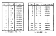
変換器31は入力されたキーナンバ信号の整数部 keynoを12で割り、その商の整数部oct 及び余りnoteを出力する除算回路あるいは変換テーブルである。周波数ナンバテーブル32は、図4(a)にその記憶内容を示すように、note番号に対応した12個の周波数ナンバFを記憶している変換テーブルである。シフト回路33は、周波数ナンバFを入力し、oct から8(=Ks/12)を引いた値だけ右ビットシフトした値を出力する。例えばキーナンバ信号として56(A3)が入力された場合には、oct が4、noteが9となる。従って、周波数ナンバテーブル32からは1.6817…というF値が出力され、シフト回路33によって4−8=−4ビット右シフト、即ち4ビット左シフト(2の4乗で除算)されて、0.1051…という周波数ナンバ値が出力される。
【0012】
キーナンバ信号の小数部Fracは、例えば7ビットの2進数で表され、指数変換テーブル30は、この7ビットの2進数をアドレスとして、[2のFrac/(12*128) 乗]を出力する。図4(b)は、指数変換テーブル30の記憶内容を示す説明図である。この図においては、Fracをアドレスを表す7ビットの整数値と見なして表現してある。中央のセント(cent)はFracを百分率で示した場合の対応する値が示されており、例えばFrac値3(0000011)は2.34セント、即ち0.0234に対応する。乗算器34は、シフト回路33の出力と指数変換テーブル30の出力値とを乗算し、入力されたキーナンバ信号に対応する周波数ナンバ値Fを出力し、保持する。
【0013】
累算器35は、加算器36、保持回路37、アンド回路38等からなり、入力された周波数ナンバ値をサンプリング周期毎に累算して波形メモリ21に対する読み出しアドレスの下位ビットを出力する。エッジ検出器39は、通常は1を出力しており、キーオン信号の立ち上がりエッジ(0から1への変化点)を検出した場合には1周期のみ出力を0にする。CPU1は、キーナンバ信号を楽音発生回路6に設定し、加算器36に乗算器34から周波数ナンバ値が入力された後にキーオン信号を立ち上げる。すると、アンド回路38から加算器36への入力が0となり、加算器36の出力は周波数ナンバ値となり、該値が保持回路37に保持される。その後はエッジ検出器39の出力が1となるので、保持回路37の記憶値が加算器36に入力され、乗算器34から入力される周波数ナンバ値と加算されて、再び保持回路37に記憶される。従って、累算器35からは読み出し周期毎に周波数ナンバ値だけ増加するアドレス信号が順次出力される。なお、実際には補間演算を行うために、累算器35の出力部に図示しない+1加算器が設けられており、加算器36から出力されるアドレス値及び該アドレス値に1を加算した値が時分割出力される。
【0014】
波形選択器40は、例えば変換テーブルから成り、音色情報、キーナンバ信号の上位ビット、あるいはタッチ情報等を入力し、波形メモリ中の波形を選択するための波形読み出しアドレスの上位ビットを出力する。なお波形選択器の出力をキーオン時に保持回路37にセットするような構成であってもよい。波形メモリ21は累算器35から出力される読み出しアドレスの整数部および波形選択器40から出力される上位アドレスに基づき、波形データを順次出力し、補間回路22は波形メモリ21から出力される2つの波形データおよび累算器35から出力される読み出しアドレスの小数部データに基づき、周知の補間演算を行う。以上のような構成により、少ない容量の変換テーブルによって精度の高い周波数ナンバへの変換が可能となる。
【0015】
上記例においては、キーナンバKをK=12*oct+note+Fracと表し、noteは余りの整数部(0≦note≦11)、Fracは余りの小数部(0≦Frac<1)であるとしたが、noteとFracの分割の仕方は任意であり、例えば2進数で表したKの小数点以下2ビットまでをnoteとし、小数点以下3〜7ビットをFracとしてもよい。この場合には、周波数ナンバテーブル32に記憶される周波数ナンバ個数が4倍の48個となるが、指数変換テーブル30の指数データ個数は1/4の32個となり、両テーブルの合計データ個数は80個となって、第1の実施例より減少する。また、シフト回路33は乗算機能を果たしているので、乗算器34の後ろに配置しても結果は同じである。
【0016】
図5は、指数変換テーブル30を他の用途にも兼用した、本発明における波形読み出し回路20の実施例を示すブロック図である。なお、図1、3と同じ機能のブロックには同じ番号が付与してある。前記例と異なるところは、指数変換テーブルの前に選択器50が設けられ、後ろに保持回路51、52が設けられたところである。周波数ナンバ変換処理時には、選択器50はキーナンバ信号を選択、出力し、指数変換テーブル30によって指数変換された値は保持回路51に保持される。
【0017】
一方、エンベロープ信号の演算に使用される時には、選択器50からはエンベロープ発生器24の信号が出力され、指数変換された値は保持回路52に保持され、加算器53によって−1が加算されて、4ビットシフタ54により左4ビットシフトされて選択器55に出力される。指数変換テーブル30には、図4(b)に示すような指数データが記憶されており、このままでは、例えば0から1の間の値を取る入力値を同じく0から1の間の値を取る指数値に変換することはできない。そこで、指数変換テーブル30の出力値から1を減算し、4ビットシフト(16倍)することによって、出力範囲がほぼ0から1の間に収まるようになる(実際は0〜0.94376…の間である)。ここで、エンベロープ発生器24から例えば0から1の間の値を取る三角波を発生し、下りの時には選択器55が4ビットシフタ54からの信号を出力するように選択器55を制御すれば、選択器55の出力には、上昇時には直線的に上昇し、下降時には指数関数的に減少するエンベロープ波形が得られる。
【0018】
図6は、図5の実施例の変形例の要部を示すブロック図である。前記実施例においては、エンベロープ発生器24の出力を指数変換テーブルを用いて変換する例を開示したが、この変形例は、エンベロープ発生器24の内部において、スピードパラメータの変換に指数変換テーブル30を用いた例である。図6の端子A及びBが、図5のエンベロープ発生器24、選択器55の代わりに、読み出しアドレス発生回路の端子A、Bにそれぞれ接続される。図6のエンベロープ発生回路は、図示するような構成によって、En+1 =En +S*(T−En )という演算を行い、目標値Tに漸近するエンベロープ信号En を発生する。スピードパラメータは指数変換されることにより、スピードの小さい部分がより詳細に設定可能となり、精度が向上する。
【0019】
以上、実施例を説明したが、次のような変形例も考えられる。前記実施例においては、指数変換テーブルを他の用途と兼用する例を開示したが、前記したように、周波数ナンバテーブルの精度を上げることも可能であり、例えばキーナンバ信号の小数点以下3ビットまで周波数ナンバテーブルで変換するようにすれば、0から96(12×8)までの値に対応して1〜2の間の値を取る指数を出力する変換テーブルが得られ、このテーブルを他の用途に兼用してもよい。このようにすれば4ビットシフタ54は不要となる。
【0020】
【発明の効果】
以上述べたように、本発明においては、周波数ナンバ変換手段は、例えばキーナンバの整数部に対応する12個の周波数ナンバのみを変換すればよく、また指数変換手段は、例えば小数点以下7ビットまでに対応する128個の指数データに変換できればよいので、変換手段をテーブルによって構成した場合には該テーブルの記憶容量が従来例に較べて非常に小さくなるという効果がある。また、変換手段は時分割で使用することによって、例えばエンベロープ信号の発生のための演算等の他の用途にも兼用でき、ハードウェアを削減させることができるという効果もある。
【図面の簡単な説明】
【図1】図3の波形読み出し回路20の構成を示すブロック図である。
【図2】本発明の前提となる電子楽器の回路構成の一例を示すブロック図である。
【図3】図2の楽音発生回路6の構成を示すブロック図である。
【図4】各テーブルの内容を示す説明図である。
【図5】指数変換テーブルを兼用した本発明の実施例を示すブロック図である。
【図6】図5の実施例の変形例の要部を示すブロック図である。[0001]
[Industrial applications]
The present invention relates to an electronic musical instrument, and more particularly to an electronic musical instrument provided with a waveform readout circuit capable of reducing a memory capacity.
[0002]
[Prior art]
2. Description of the Related Art Conventionally, in an electronic musical instrument such as an electronic piano using a tone generation circuit of a waveform reading method, a waveform corresponding to a specific pitch is recorded by PCM for each tone, and processed waveform data is stored in a waveform memory. The waveform is read out at an address interval proportional to the pitch to be sounded, and the address interval data is called a frequency number. Conventionally, in order to convert a key number corresponding to each key of a semitone unit of a keyboard into a frequency number, a conversion table that stores a frequency number corresponding to each key number has been used. However, this method has a problem that it is necessary to store a large number of frequency numbers corresponding to the number of keys. To solve this problem, for example, as described in JP-A-2-139599. Technologies have been proposed. This method focuses on the fact that the frequency number doubles each time the octave increases, converts the key number into octave information and note (note name) information, converts the note information into a frequency number, and responds to the octave information. Thus, a desired frequency number is obtained by bit shifting.
[0003]
[Problems to be solved by the invention]
In the conventional frequency number conversion method as described above, when obtaining a frequency number in semitone units, it is sufficient to store 12 frequency numbers in one octave. In order to cope with the frequency change, it is necessary to perform control in units of cents in which a semitone is divided into, for example, 100. If the frequency numbers corresponding to all cents are stored, the storage capacity becomes extremely large. Was.
SUMMARY OF THE INVENTION It is an object of the present invention to provide an electronic musical instrument having a tone generating means capable of coping with a fine frequency change with a small storage capacity by improving the above-mentioned problems of the prior art.
[0004]
[Means for Solving the Problems]
According to the present invention, first conversion means for inputting upper digit information of pitch information and performing exponential conversion,
The lower digit information excluding the upper digit information of the pitch information is input and multiplied by the second converting means for performing exponential conversion, the output information of the first converting means and the output information of the second converting means. Multiplication means for calculating a frequency number for reading a waveform from the waveform memory, wherein at least one of the first conversion means and the second conversion means performs exponential conversion of information other than the pitch information. It is also used as conversion means for performing the conversion.
[0005]
[Action]
According to the present invention, with the above-described configuration, the frequency number conversion means only needs to convert, for example, only 12 frequency numbers corresponding to the integer part of the key number, and the exponent conversion means has, for example, two digits after the decimal point (centennial). It is only necessary to convert the data into 100 or 128 exponent data corresponding to up to 7 bits after the decimal point in binary or binary. Therefore, when the conversion means is constituted by a table, the storage capacity of the table is smaller than that of the conventional example. Very small. Further, by using the conversion means in a time-sharing manner, it can be used for other purposes such as calculation for generating an envelope signal.
[0006]
【Example】
Hereinafter, an embodiment of the present invention will be described in detail with reference to the drawings. FIG. 2 is a block diagram showing an example of a circuit configuration of an electronic musical instrument on which the present invention is based . The
[0007]
As will be described later, the musical
[0008]
FIG. 3 is a block diagram showing the configuration of the
[0009]
The
[0010]
FIG. 1 is a block diagram showing a configuration of the
[0011]
The
[0012]
The decimal part Frac of the key number signal is represented by, for example, a 7-bit binary number, and the exponent conversion table 30 outputs [2 to the power of Frac / (12 * 128)] using the 7-bit binary number as an address. FIG. 4B is an explanatory diagram showing the storage contents of the exponent conversion table 30. In this figure, Frac is represented as a 7-bit integer value representing an address. The center cent indicates the corresponding value when Frac is expressed as a percentage, for example, a Frac value of 3 (0000011) corresponds to 2.34 cents, or 0.0234. The
[0013]
The
[0014]
The
[0015]
In the upper clean, it represents the key number K with K = 12 * oct + note + Frac, note the remainder of the integer part (0 ≦ note ≦ 11), was a Frac is less of the fraction (0 ≦ Frac <1), The method of dividing note and Frac is arbitrary. For example, note may be up to 2 bits after the decimal point of K represented by a binary number, and Frac may be 3 to 7 bits after the decimal point. In this case, the number of frequency numbers stored in the frequency number table 32 is quadrupled to 48, but the number of exponent data in the exponent conversion table 30 is 1/4, 32, and the total number of data in both tables is The number is 80, which is smaller than in the first embodiment. Further, since the
[0016]
5, the exponential conversion table 30 were also combined in other applications, a block diagram illustrating a real施例waveform readout
[0017]
On the other hand, when the signal is used for calculating the envelope signal, the signal of the
[0018]
Figure 6 is a block diagram showing the main parts of a modification of the embodiment of FIG. In the above-described embodiment, an example in which the output of the
[0019]
The embodiments have been described above, but the following modifications are also conceivable. In the above-described embodiment, an example in which the exponential conversion table is used for other purposes is disclosed. However, as described above, it is also possible to increase the accuracy of the frequency number table. If conversion is performed using a number table, a conversion table that outputs an exponent that takes a value between 1 and 2 corresponding to a value from 0 to 96 (12 × 8) can be obtained. May also be used. In this case, the 4-
[0020]
【The invention's effect】
As described above, in the present invention, the frequency number converting means only needs to convert, for example, only 12 frequency numbers corresponding to the integer part of the key number, and the exponential converting means has, for example, 7 bits after the decimal point. Since it is only necessary to convert the data into the corresponding 128 index data, when the conversion means is constituted by a table, there is an effect that the storage capacity of the table becomes very small as compared with the conventional example. Further, by using the conversion means in a time-sharing manner, the conversion means can also be used for other purposes such as an operation for generating an envelope signal, and there is an effect that hardware can be reduced.
[Brief description of the drawings]
FIG. 1 is a block diagram showing a configuration of a
FIG. 2 is a block diagram showing an example of a circuit configuration of an electronic musical instrument on which the present invention is based .
FIG. 3 is a block diagram showing a configuration of a
FIG. 4 is an explanatory diagram showing the contents of each table.
FIG. 5 is a block diagram showing an embodiment of the present invention which also serves as an exponential conversion table.
FIG. 6 is a block diagram showing a main part of a modification of the embodiment of FIG . 5 ;
Claims (3)
音高情報の内の前記上位桁情報を除く下位桁情報を入力し、指数変換する第2の変換手段と、
第1の変換手段の出力情報と第2の変換手段の出力情報とを乗算して、波形メモリから波形を読み出すための周波数ナンバを算出する乗算手段と、を備え、
前記第1の変換手段及び前記第2の変換手段の少なくとも一方は、前記音高情報以外の情報を指数変換するための変換手段としても使用されることを特徴とする電子楽器。First conversion means for inputting upper digit information of pitch information and performing exponential conversion;
Second converting means for inputting lower digit information of the pitch information excluding the upper digit information and performing exponential conversion;
Multiplying means for multiplying the output information of the first converting means and the output information of the second converting means to calculate a frequency number for reading a waveform from the waveform memory;
An electronic musical instrument, wherein at least one of the first conversion unit and the second conversion unit is also used as a conversion unit for performing exponential conversion of information other than the pitch information .
前記下位桁情報は、音高情報の内の半音未満の情報であることを特徴とする請求項1に記載の電子楽器。The upper digit information is key number information in semitone units of the pitch information,
The electronic musical instrument according to claim 1, wherein the lower digit information is information of less than a semitone in pitch information.
前記上位桁情報を、所定のオクターブとの差をオクターブ単位で表した差情報とオクターブ内の音名情報とに変換する変換手段と、
音名情報を入力して、所定のオクターブ内の音名に対応する周波数ナンバを出力する周波数ナンバテーブル手段と、
周波数ナンバテーブル手段から出力された周波数ナンバデータを前記差情報が示すビット数だけシフトするデータシフト手段とからなることを特徴とする請求項1あるいは2のいずれかに記載の電子楽器。The first conversion means includes:
Conversion means for converting the upper digit information into difference information representing a difference from a predetermined octave in octave units and note name information within the octave,
Frequency number table means for inputting note name information and outputting a frequency number corresponding to a note name within a predetermined octave,
3. The electronic musical instrument according to claim 1, further comprising data shift means for shifting the frequency number data output from the frequency number table means by the number of bits indicated by the difference information.
Priority Applications (1)
| Application Number | Priority Date | Filing Date | Title |
|---|---|---|---|
| JP08456595A JP3551992B2 (en) | 1995-03-17 | 1995-03-17 | Electronic musical instrument |
Applications Claiming Priority (1)
| Application Number | Priority Date | Filing Date | Title |
|---|---|---|---|
| JP08456595A JP3551992B2 (en) | 1995-03-17 | 1995-03-17 | Electronic musical instrument |
Publications (2)
| Publication Number | Publication Date |
|---|---|
| JPH08263067A JPH08263067A (en) | 1996-10-11 |
| JP3551992B2 true JP3551992B2 (en) | 2004-08-11 |
Family
ID=13834188
Family Applications (1)
| Application Number | Title | Priority Date | Filing Date |
|---|---|---|---|
| JP08456595A Expired - Fee Related JP3551992B2 (en) | 1995-03-17 | 1995-03-17 | Electronic musical instrument |
Country Status (1)
| Country | Link |
|---|---|
| JP (1) | JP3551992B2 (en) |
-
1995
- 1995-03-17 JP JP08456595A patent/JP3551992B2/en not_active Expired - Fee Related
Also Published As
| Publication number | Publication date |
|---|---|
| JPH08263067A (en) | 1996-10-11 |
Similar Documents
| Publication | Publication Date | Title |
|---|---|---|
| US4875400A (en) | Electronic musical instrument with touch response function | |
| KR0135601B1 (en) | Digital signal generator for electronic instruments | |
| JPH079588B2 (en) | Musical sound generator | |
| JP3404794B2 (en) | Waveform generator | |
| EP0454047A2 (en) | Tone generation apparatus | |
| US5637821A (en) | Storing and interpolating means for a musical sound generating device | |
| EP0169659B1 (en) | Sound generator for electronic musical instrument | |
| JP2605916B2 (en) | Waveform signal generator | |
| JPH0642149B2 (en) | Electronic musical instrument | |
| US5428183A (en) | Tone signal generating apparatus for performing a timbre change by storing a full frequency band in a wave memory | |
| JP2766662B2 (en) | Waveform data reading device and waveform data reading method for musical sound generator | |
| JPH0563799B2 (en) | ||
| JP2599193B2 (en) | Music information expression method and music information expression device | |
| US5218155A (en) | Tone signal processing apparatus for PCM waveform interpolation and filtering | |
| JP2580814B2 (en) | Music signal generator | |
| JPH0535277A (en) | Electronic musical instrument | |
| JPH08263067A (en) | Electronic musical instrument | |
| JPS61124994A (en) | Musical sound signal generator | |
| JP2861007B2 (en) | Electronic musical instrument | |
| US5464947A (en) | Apparatus for and method of producing fluctuations in sound for electronic sound system | |
| JP2880720B2 (en) | Musical sound wave type reading device | |
| JPH043556B2 (en) | ||
| JPS5839B2 (en) | electronic musical instruments | |
| JP3044712B2 (en) | Electronic musical instrument | |
| JP3095323B2 (en) | Electronic musical instrument |
Legal Events
| Date | Code | Title | Description |
|---|---|---|---|
| A61 | First payment of annual fees (during grant procedure) |
Free format text: JAPANESE INTERMEDIATE CODE: A61 Effective date: 20040420 |
|
| R150 | Certificate of patent or registration of utility model |
Free format text: JAPANESE INTERMEDIATE CODE: R150 |
|
| LAPS | Cancellation because of no payment of annual fees |