JP3558905B2 - Method for manufacturing flip-chip type semiconductor device and semiconductor manufacturing apparatus - Google Patents
Method for manufacturing flip-chip type semiconductor device and semiconductor manufacturing apparatus Download PDFInfo
- Publication number
- JP3558905B2 JP3558905B2 JP36710898A JP36710898A JP3558905B2 JP 3558905 B2 JP3558905 B2 JP 3558905B2 JP 36710898 A JP36710898 A JP 36710898A JP 36710898 A JP36710898 A JP 36710898A JP 3558905 B2 JP3558905 B2 JP 3558905B2
- Authority
- JP
- Japan
- Prior art keywords
- semiconductor element
- circuit board
- resin
- liquid resin
- outer periphery
- Prior art date
- Legal status (The legal status is an assumption and is not a legal conclusion. Google has not performed a legal analysis and makes no representation as to the accuracy of the status listed.)
- Expired - Fee Related
Links
Images


Classifications
-
- H—ELECTRICITY
- H10—SEMICONDUCTOR DEVICES; ELECTRIC SOLID-STATE DEVICES NOT OTHERWISE PROVIDED FOR
- H10W—GENERIC PACKAGES, INTERCONNECTIONS, CONNECTORS OR OTHER CONSTRUCTIONAL DETAILS OF DEVICES COVERED BY CLASS H10
- H10W74/00—Encapsulations, e.g. protective coatings
- H10W74/10—Encapsulations, e.g. protective coatings characterised by their shape or disposition
- H10W74/15—Encapsulations, e.g. protective coatings characterised by their shape or disposition on active surfaces of flip-chip devices, e.g. underfills
Landscapes
- Wire Bonding (AREA)
- Encapsulation Of And Coatings For Semiconductor Or Solid State Devices (AREA)
Description
【0001】
【発明の属する技術分野】
本発明は、フリップチップ型半導体装置の半導体素子と回路基板との間に樹脂充填を行う方法及びこの方法を実施する半導体製造装置に関するものである。
【0002】
【従来の技術】
フリップチップ型半導体装置は、半導体素子とこの半導体素子が搭載された回路基板から構成されている。図11は、従来のフリップチップ型半導体装置の製造工程を説明する製造工程の断面図である。集積回路が内部に形成された半導体素子1にはこの集積回路に電気的に接続された複数の接続電極(図示せず)が形成されている。この接続電極には、例えば、はんだから構成されたボール状の接続端子(バンプ)2が接続されている。回路基板3は、半導体素子1が搭載される主面には配線及び接続電極(図示せず)が形成されている。そして、複数のバンプ2が主面の接続電極に接続されている。回路基板3の裏面には、接続電極 (図示せず)が形成されており、この接続電極に接続されるようにボール状の外部端子7が取り付けられている。回路基板3の主面の接続電極と裏面の接続電極とは適宜回路基板3の内部配線(図示せず)を介して接続されている。半導体素子1と回路基板3との間にはバンプ2の厚さ分だけ間隙がある。この間隙にはエポキシ樹脂などの樹脂が封止されている。
【0003】
【発明が解決しようとする課題】
図11を参照してフリップチップ型半導体装置に樹脂を充填する方法を説明する。半導体素子1に取り付けたバンプ2を回路基板3に搭載してから、半導体素子1と回路基板3との間隙に半導体素子1の外周の一部にディスペンスノズル4から液状樹脂5を滴下する(図11(a))。この加熱軟化した液状樹脂5を毛細管現象により半導体素子1と回路基板3の間隙に浸透させる(図11(b))。液状樹脂5は、半導体素子1と回路基板3の間隙に均一に広がり、加熱硬化されて樹脂封止体6が形成される(図11(c))。
【0004】
この様に半導体素子1と回路基板3との間隙への樹脂充填が終了した後、樹脂封止体を形成するため、あらかじめ塗布しなかった一部に再度液状樹脂を塗布していた。この場合樹脂塗布工程に要する時間は、塗布装置を1台で補おうとした場合、塗布時間のみならず半導体素子外周より回路基板の間隙に樹脂を充填する時間も合計されたものとなり、生産性が非常に低い樹脂充填装置となる。充填時間は、半導体素子外周をより大きく囲い込むように塗布することで、短縮できるがあまり大きく囲い過ぎると、外周からの回り込みにより内部に空気を巻き込んでしまう。従って、現実的に可能な塗布領域は半導体素子外周の50%以下になる。これは断続的な塗布を行ったときでも同様であり、要するに半導体素子の中心から見て180度以上の角度に樹脂が塗布されてしまうと、空気の巻き込みが生じてしまうという問題があった。
本発明は、このような事情によりなされたものであり、従来に比べて短時間で樹脂充填が実現でき、且つ空気の巻き込みや樹脂から発生するガスなどによるボイド不良が低減できるフリップチップ型半導体装置の製造方法及びこの方法に用いる半導体製造装置を提供する。
【0005】
【課題を解決するための手段】
本発明は、フリップチップ型半導体装置の半導体素子と回路基板との間隙及びその外周への樹脂充填方法において、液状樹脂を半導体素子外周に塗布し、外周の1部は排気孔として液状樹脂を塗布せずにおいて真空チャンバへセットし、真空チャンバ内を、例えば、2torr以下に減圧し、減圧直後に排気孔を強制的に閉鎖した後、真空破壊を実施して半導体素子内外の気圧差(例えば、約1気圧)を利用し樹脂充填させることを特徴としている。また、フリップチップ型半導体装置の樹脂充填装置において、半導体素子外周の少なくとも一部を残して液状樹脂を塗布する手段と、半導体装置を減圧下にさらす手段と、減圧下で半導体素子外周の少なくとも一部の未塗布部分を強制的に塞ぐ手段と、減圧下で所定時間加熱する手段とを具備したことを特徴とする。
従来技術に比べて減圧直後に排気孔を強制的に閉鎖するので極めて短時間でフリップチップ型半導体装置の樹脂充填が実現でき、また、空気の巻き込みや樹脂から発生するガスなどによるボイド不良も低減できる。
【0006】
本発明の半導体装置の製造方法は、主面に形成された接続電極にボール状接続端子が設けられた半導体素子をこのボール状接続端子を介して接続された回路基板を塗布装置に搭載する工程と、前記回路基板上の前記半導体素子外周の少なくとも一部を残して液状樹脂を塗布する工程と、前記半導体素子と前記回路基板とを減圧下に置いて、前記半導体素子と前記回路基板との間隙の空気を排除すると共に残された未塗布部を、垂直もしくは、水平に可動するシャフト及びその先端に設けられたスキージからなる手段、もしくは垂直に可動するヘッド及びその先端に接するテープからなる手段により、強制的に塞ぎ、前記半導体素子の全外周を前記液状樹脂で充填させる工程と、前記液状樹脂が充填された前記半導体素子と前記回路基板とを大気圧に戻して前記半導体素子と前記回路基板との間隙の未充填部分の樹脂充填を完了させる工程とを備えていることを特徴としている。前記回路基板上の前記半導体素子外周の少なくとも一部を残して液状樹脂を塗布する工程は大気圧中で行われるようにしても良い。強制的に塞ぐ手段にテープを用いると常に綺麗な面で排気孔を塞ぐことができ塞いだ所の外観が綺麗になるという利点がある。
【0007】
本発明の半導体製造装置は、主面に形成された接続電極にボール状接続端子が設けられた半導体素子をこのボール状接続端子を介して接続された回路基板を塗布装置に搭載する手段と、前記回路基板上の前記半導体素子外周の少なくとも一部を残して液状樹脂を塗布する手段と、前記半導体素子と前記回路基板とを減圧下に置いて、前記半導体素子と前記回路基板との間隙の空気を排除すると共に残された未塗布部を強制的に塞ぎ、前記半導体素子全外周を前記液状樹脂で充填させる手段と、前記液状樹脂が充填された前記半導体素子と前記回路基板とを大気圧に戻して前記半導体素子と前記回路基板との間隙の未充填部分の樹脂充填を完了させる手段とを備え、前記未塗布部を強制的に塞ぐ手段は、垂直もしくは、水平に可動するシャフト及びその先端に設けられたスキージからなることを特徴としている。
また、本発明の半導体製造装置は、主面に形成された接続電極にボール状接続端子が設けられた半導体素子をこのボール状接続端子を介して接続された回路基板を塗布装置に搭載する手段と、前記回路基板上の前記半導体素子外周の少なくとも一部を残して液状樹脂を塗布する手段と、前記半導体素子と前記回路基板とを減圧下に置いて、前記半導体素子と前記回路基板との間隙の空気を排除すると共に残された未塗布部を強制的に塞ぎ、前記半導体素子全外周を前記液状樹脂で充填させる手段と、前記液状樹脂が充填された前記半導体素子と前記回路基板とを大気圧に戻して前記半導体素子と前記回路基板との間隙の未充填部分の樹脂充填を完了させる手段とを備え、前記未塗布部を強制的に塞ぐ手段は、垂直に可動するヘッド及びその先端に接するテープからなることを特徴としている。前記半導体素子と前記回路基板との間隙の空気を排除すると共に残された未塗布部を強制的に塞ぎ、前記半導体素子全外周を前記液状樹脂で充填させる手段は、減圧反応室に配置されているようにしても良い。
【0008】
なお液状樹脂の粘度は、ディスペンス時には10〜100000pois程度が適当である。半導体素子の周辺に塗布される液状樹脂に設けられた排気孔として用いられる未塗布部分のトータルの大きさは、半導体素子の5%〜70%が適当である。5%未満では、排気孔としての効果はなく、70%を越えると減圧空間を形成することができない。また、半導体素子と回路基板との間隙は20〜200μm程度である。回路基板は、セラミックスもしくは合成樹脂を材料にしている。さらに、液状樹脂は、エポキシ系樹脂、シリコーン系樹脂、ビニル重合樹脂、フェノール樹脂、不飽和ポリエステル樹脂、ジアリルフタレート樹脂などの熱硬化性樹脂、芳香族ポリアミド、ナイロン樹脂、超高分子量ポリエチレン、オレフィンやアミドなどを使用した熱可塑性エラストマーなどの熱可塑性樹脂などが用いられる。
【0009】
【発明の実施の形態】
以下、図面を参照して発明の実施の形態を説明する。
まず、図1乃至図4を参照して第1の実施例を説明する。
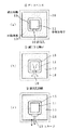
図1は、樹脂充填方法を説明するフリップチップ型半導体装置の平面図、図2は、樹脂充填方法を説明する樹脂が充填された回路基板の平面図、図3は、半導体素子外周に樹脂が塗布された半導体装置の斜視図及び側面図、図4は、半導体素子外周の樹脂を繋ぐ方法を説明する半導体装置の側面図である。
フリップチップ型半導体装置は、半導体素子11と、この半導体素子が搭載された回路基板13と、両者の間に形成された樹脂封止体とから構成されている。すなわち、集積回路が内部に形成された半導体素子11にはこの集積回路に電気的に接続された複数の接続電極が形成されている。この接続電極には、例えば、はんだからなるボール状の接続端子(バンプ)が接続されている。回路基板13の半導体素子11が搭載される主面には配線及び接続電極が形成されている。半導体素子11の複数のバンプは、回路基板13主面の接続電極に接続されている。回路基板13の裏面には、接続電極が形成されており、この接続電極に接続されるように図11(c)に示される従来のフリップチップ型半導体装置と同じ様にボール状の外部端子が取り付けられている。
【0010】
回路基板13の主面の接続電極と裏面の接続電極とは適宜回路基板13の内部配線を介して接続されている。また、半導体素子11と回路基板13との間にはバンプの厚さ分だけ間隙がある。この間隙にはエポキシ樹脂などの樹脂が封止されており、図1及び図2は、この樹脂の間隙への充填方法が示されている。
▲1▼ この回路基板13上の半導体素子11外周に樹脂が塗布されていない部分を一部残してディスペンサーから供給される液状樹脂15をディスペンスする。樹脂が塗布されていない部分は、排気孔10として用いられる(図1(a)、図3(a)、(b))。すなわち、半導体素子11外周の一部を残して全体を囲い込む様に液状樹脂15を塗布する。ここで、半導体素子11外周の一部に樹脂を塗布しない理由は、後述の減圧工程において、半導体素子と回路基板の間の空気を排気するためである。▲2▼ その後、半導体装置全体を減圧雰囲気下にさらすことにより、半導体素子外周部が塗布されていない部分を介して、半導体素子11と回路基板13との間の空気を排気する。この際、充分な排気を実現するためには半導体素子外周の樹脂が塗布されていない部分を所定時間残存させておく事が有効である。半導体装置を減圧下にさらすことは、真空チャンバ18で行う(図1(b))。
【0011】
▲3▼ その後、真空チャンバ18において真空もしくは減圧下で、半導体装置の半導体素子外周部が塗布されていない部分の排気孔10を、半導体装置と水平方向に動作するシャフトの先端に設けられたスキージ19により、その周辺の液状樹脂15を揺動・撹拌し、半導体素子11の外周の液状樹脂15を繋げる(図1(c))。塗布されていない部分を確実且つ短時間で繋げることが可能である。
▲4▼ 半導体素子11の液状樹脂が完全に繋がった後の半導体素子11と回路基板13との間の半導体素子11中央に存在する樹脂未充填部分は、閉じた減圧空間101になっている。次に、真空チャンバ18を大気圧状態にする、すなわち、閉じた減圧空間101が存在する状態で回路基板13及び液状樹脂15の周囲を大気雰囲気に開放すると、内部の減圧空間とその外周との間に気圧差が生じるので液状樹脂15外周全体に掛かる大気圧により減圧空間101が潰れて半導体素子11と回路基板13との間隙の内部まで確実に充填がなされる(図2(a))。大気圧は、900〜1060hPa程度をいう。その後、半導体装置を真空チャンバ18から取り出す(図2(b))。次に、▲5▼ 液状樹脂を加熱硬化させて半導体素子と回路基板13との間に充実した樹脂封止体16を形成する。
【0012】
次に、図4を参照しながら半導体素子外周の樹脂を繋ぐ動作を詳細に説明する。まず▲1▼ 真空チャンバ内を減圧状態にして、真空チャンバに取り付けたシャフト(図示せず)を操作してスキージ19を回路基板13上の半導体素子11外周に塗布形成した液状樹脂15に設けられた排気孔10目指して下降させる(図4(a))。▲2▼ 次に、下降したスキージ19が排気孔10を塞ぎ、さらに排気孔10の周辺の液状樹脂15を揺動・撹拌し、半導体素子11の外周の液状樹脂15を繋げる(図2(b))。▲3▼ その後、排気孔を潰して液状樹脂15を繋げてからスキージ19を上昇させる。
液状樹脂が塗布されていない部分を確実且つ短時間で繋げることが可能であり、従来技術に比べ極めて短時間でフリップチップ型半導体装置の樹脂充填が実現できる。また、樹脂充填は、減圧下でなされるため空気の巻き込みや樹脂から発生するガスなどによるボイド不良も低減できる。
【0013】
次に、図5を参照して第2の実施例を説明する。
この実施例は、排気孔を塞ぐ手段としてテープとこれを駆動するヘッドを利用して液状樹脂を繋ぐことに特徴がある。図5は、半導体素子外周の樹脂を繋ぐ方法を説明する半導体装置の側面図である。
フリップチップ型半導体装置は、半導体素子21と、この半導体素子21が搭載された回路基板23と、両者の間に形成された樹脂封止体とから構成されている。すなわち、集積回路が内部に形成された半導体素子21にはこの集積回路に電気的に接続された複数の接続電極が形成されている。この接続電極には、例えば、はんだからなるボール状のバンプが接続されている。回路基板23の半導体素子21が搭載される主面には配線及び接続電極が形成されている。半導体素子21の複数のバンプは、回路基板13主面の接続電極に接続されている。回路基板23の裏面には、接続電極が形成されており、この接続電極に接続されるように図11(c)に示される従来のフリップチップ型半導体装置と同じ様にボール状の外部端子が取り付けられている。回路基板23の主面の接続電極と裏面の接続電極とは適宜回路基板23の内部配線を介して接続されている。また半導体素子21と回路基板23との間にはバンプの厚さ分だけ間隙がある。この間隙には液状樹脂から形成されたエポキシ樹脂などの樹脂封止体が充填されている。
【0014】
次に、フリップチップ型半導体装置の樹脂封止体を形成するために行われる液状樹脂の回路基板への塗布について説明する。
液状樹脂25の塗布は、回路基板23にフリップチップ接合された半導体素子21外周の一部を残して全体を囲い込む様に行われる。半導体素子外周の一部に設けた樹脂を塗布しない部分は、後述の減圧工程における半導体素子と回路基板の間の空気を排気するための排気孔20として用いられる。
▲1▼ このように液状樹脂25を排気孔20を有するように塗布した回路基板23を減圧状態にされた真空チャンバ(図示しない)内に収容する。真空チャンバには、排気孔20上方に位置するように、テープ送り27、このテープ送りに支持されて移動するテープ28及び上下に移動しこのテープを排気孔20の方向に押し付けるヘッド26とが形成配置されている。まず、排気孔20の上部からヘッド26が樹脂接触用のテープ28を押し出しながら下降させて、これを液状樹脂が塗布されていない部分である排気孔20の周辺の液状樹脂25に接触させる(図5(a))。そして、液状樹脂25と接触後、テープ送り機構27の水平動作によりテープ28は液状樹脂25上を移動して半導体素子21外周の液状樹脂25を繋げる。
【0015】
そして排気孔20は、閉鎖される(図5(b))。半導体素子21外周の液状樹脂25が繋がり、排気孔20が閉鎖されてから、ヘッド26を上昇させてテープ28を液状樹脂25から隔離する(図5(c))。
半導体素子の液状樹脂が完全に繋がった後の半導体素子と回路基板との間の半導体素子中央に存在する樹脂未充填部分は、閉じられた減圧空間になっている。この状態で真空チャンバを大気圧状態にする、すなわち、閉じた減圧空間が存在する状態で回路基板及び液状樹脂の周囲を大気雰囲気に開放すると、内部の減圧空間とその外周との間に気圧差が生じるので液状樹脂の全体に掛かる大気圧により減圧空間が潰れて半導体素子と回路基板との間隙の内部まで確実に充填がなされる。次に、液状樹脂が加熱硬化されて半導体素子と回路基板との間に充実した樹脂封止体が形成される。その後、半導体装置を真空チャンバから取り出す。
【0016】
液状樹脂の塗布されていない部分を確実且つ短時間で繋げることが可能である。半導体素子の樹脂が完全に繋がった後の半導体素子と回路基板の間の樹脂未充填部分は閉じた減圧空間になっており、この状態で半導体装置の周囲を大気雰囲気に開放すると、内部減圧空間との間に気圧差が生じる為、液状樹脂外周全体に掛かる大気圧により内部の充填がなされる。
液状樹脂が塗布されていない部分を確実且つ短時間で繋げることが可能であり、従来技術に比べ極めて短時間でフリップチップ型半導体装置の樹脂充填が実現できる。また、樹脂充填は、減圧下でなされるため空気の巻き込みや樹脂から発生するガスなどによるボイド不良も低減できる。
【0017】
次に、図6を参照して第3の実施例を説明する。
この実施例は、排気孔を塞ぐ手段として当接面が櫛歯状になっているスキージを利用して液状樹脂を繋ぐことに特徴がある。図6は、半導体素子外周の樹脂を繋ぐ方法を説明する半導体装置の平面図及びこの方法に用いるスキージの斜視図である。
フリップチップ型半導体装置は、半導体素子31と、この半導体素子31が搭載された回路基板33と、両者の間に形成された樹脂封止体とから構成されている。すなわち、集積回路が内部に形成された半導体素子31には主面にこの集積回路に電気的に接続された複数の接続電極が形成されている。この接続電極には、例えば、はんだからなるボール状のバンプが接続されている。回路基板33の半導体素子31が搭載される主面には配線及び接続電極が形成されている。半導体素子31の複数のバンプは、回路基板33主面の接続電極に接続されている。回路基板33の裏面には、接続電極が形成されており、この接続電極に接続されるように図11(c)に示される従来のフリップチップ型半導体装置と同じ様にボール状の外部端子が取り付けられている。
【0018】
回路基板33の主面の接続電極と裏面の接続電極とは適宜回路基板33の内部配線を介して接続されている。また半導体素子31と回路基板33との間にはバンプの厚さ分だけ間隙がある。この間隙には液状樹脂から形成されたエポキシ樹脂などの樹脂封止体が充填されている。
次に、フリップチップ型半導体装置の樹脂封止体を形成するために行われる液状樹脂の回路基板への塗布について説明する。
液状樹脂35の塗布は、回路基板33にフリップチップ接合された半導体素子31外周の一部を残して全体を囲い込む様に行われる。半導体素子外周の一部に設けた樹脂を塗布しない部分は、後述の減圧工程における半導体素子と回路基板の間の空気を排気するための排気孔30として用いられる。
【0019】
▲1▼このように液状樹脂35を排気孔30を有するように塗布した回路基板33を減圧状態にされた真空チャンバ(図示しない)内に収容する。真空チャンバには、シャフトの先端に設けたスキージ36が装着されている。まず真空チャンバの上方に配置されたスキージ36を回路基板33の主面近くまで下降させる(図6(a))。次に、▲2▼スキージ36を半導体素子31の排気孔30が形成された辺に沿って平行に所定の間隔で矢印の方向に移動させて排気孔30を液状樹脂25で塞ぐ(図6(b))。次に、▲3▼矢印に示すようにスキージ36を半導体素子31の排気孔30が形成された辺に垂直にこの辺に近ずくように移動させる(図6(c))。そして、▲4▼矢印に示すように、前記排気孔30がある辺に水平に▲2▼工程とは逆方向にこの辺に近接させて移動させる。この移動により排気孔30は完全に塞がれる(図6(d))。その後、▲5▼スキージ36を真空チャンバの上方に移動させる。
【0020】
他の実施例と同様に、半導体素子の液状樹脂が完全に繋がった後の半導体素子と回路基板との間にあって、半導体素子中央に存在する樹脂未充填部分は、閉じられた減圧空間になっている。この状態で真空チャンバを大気圧状態にする、すなわち、閉じた減圧空間が存在する状態で回路基板及び液状樹脂の周囲を大気雰囲気に開放すると、内部の減圧空間とその外周との間に気圧差が生じるので液状樹脂の全体に掛かる大気圧により減圧空間が潰れて半導体素子と回路基板との間隙の内部まで確実に充填がなされる。次に、液状樹脂が硬化されて半導体素子と回路基板との間に充実した樹脂封止体が形成される。その後、半導体装置を真空チャンバから取り出す。
液状樹脂の塗布されていない部分を確実且つ短時間で繋げることが可能である。半導体素子の液状樹脂が完全に繋がった後の半導体素子と回路基板の間の樹脂未充填部分は閉じた減圧空間になっており、この状態で半導体装置の周囲を大気雰囲気に開放すると、内部減圧空間との間に気圧差が生じて内部への樹脂充填がなされる。また、樹脂充填は、減圧下でなされるため空気の巻き込みや樹脂から発生するガスなどによるボイド不良も低減できる。
【0021】
次に、図7及び図8を参照して第4の実施例を説明する。
図7は、本発明のフリップチップ型半導体装置の製造方法を実施するために用いられ、この半導体装置に樹脂封止体(アンダーフィル)を形成する半導体製造装置の概略断面図、図8は、樹脂封止体を形成する製造工程を示すフロー図である。
図8に示すように、回路基板に搭載された半導体素子外周に排気孔を備えるように液状樹脂を塗布してから樹脂封止体を形成するまでの工程は、以下の通りである。まず▲1▼ 回路基板とその上に搭載された半導体素子を樹脂塗布ステージにセットする。▲2▼ 樹脂塗布ステージにおいて、回路基板上の半導体素子外周に樹脂が塗布されていない部分を排気孔として一部残すようにディスペンサーから供給される液状樹脂をディスペンスする。▲3▼ その後半導体装置全体を真空チャンバに収容し、半導体素子を搭載した回路基板を加熱ステージに載置する。これにより半導体装置は減圧雰囲気下にさらされて半導体素子外周部が塗布されていない部分の排気孔を介して、半導体素子と回路基板との間の空気を排気する。この際、充分な排気を実現するためには半導体素子外周の樹脂が塗布されていない部分を所定時間残存させておくことが有効である。
【0022】
▲4▼ その後真空チャンバ内を真空ポンプを用いて減圧状態にし、この減圧下で半導体装置の半導体素子外周部が塗布されていない部分の排気孔を強制閉鎖機構で強制的に塞ぎ、半導体素子の周辺の液状樹脂を繋げる。▲5▼ 液状樹脂が完全に繋がった後の半導体素子と回路基板との間の半導体素子中央に存在する樹脂未充填部分は閉じた減圧空間になっている。そして真空チャンバを大気圧状態にすると、内部の減圧空間とその外周との間に気圧差が生じて液状樹脂外周全体に掛かる大気圧により減圧空間が潰れ、半導体素子と回路基板との間隙の内部まで確実に充填がなされる。次に、▲6▼半導体素子及び樹脂封止体を搭載させた回路基板を真空チャンバから取り出す。後に半導体素子と回路基板との間の液状樹脂はオーブンで硬化される。
【0023】
図8に示すように半導体製造装置は、塗布ステージ41と加熱ステージ42とが分離されている。そして、加熱ステージ42は、真空チャンバ40に設置されている。樹脂塗布ステージ41は、大気圧中で操作される。半導体素子を搭載した回路基板は、樹脂塗布ステージ41上で樹脂塗布を施される。液状樹脂は、X−Y−Zロボット45により制御されるディスペンサーのノズルヘッド43から回路基板上に供給される。回路基板の位置は、認識カメラ44でその位置を認識され、この認識に基づいてノズル位置補正装置46がノズルの位置を補正する。液状樹脂が塗布された回路基板は、真空チャンバ40内に搬送される。真空チャンバ40の中には加熱ステージ42の他に強制閉鎖機構47が収納されている。強制閉鎖機構47は、真空チャンバ40の内部もしくは外部で操作れる。また、当然真空ポンプ48も取り付けられている。樹脂塗布ステージで図8の▲1▼工程及び▲2▼工程が行われ、樹脂加熱ステージ41で▲3▼工程乃至▲6▼工程が行われる。
【0024】
次に、図9及び図10を参照して第5の実施例を説明する。
この実施例は、回路基板上に塗布された液状樹脂に形成された排気孔の形状に関するものである。図9及び図10は、回路基板上において半導体素子外周に塗布された液状樹脂の形状を示す半導体素子及び回路基板の平面図である。
本発明は、以上のように、フリップチップ型半導体装置の半導体素子と回路基板との間隙及びその外周へ樹脂充填し、この間隙に樹脂封止体を形成する方法において、液状樹脂を半導体素子外周に塗布し、外周の1部は排気孔として液状樹脂を塗布せずにおいて真空チャンバへセットし、真空チャンバ内を減圧し、減圧直後に排気孔を強制的に閉鎖して前記間隙に液状樹脂で構成された減圧空間を形成後、真空破壊を実施して半導体素子内外の気圧差を利用し樹脂充填させることを特徴としている。
【0025】
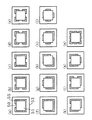
回路基板53上の半導体素子51外周に塗布された液状樹脂55の形状は、排気孔50の数、大きさを自由に変えることができる。図9は、液状樹脂の塗布形状の例を示したものである。排気孔50は、半導体素子51周辺の一か所にのみ形成する第1の実施例の場合(図9(a))に限らず、複数箇所に形成することができる(図9(b)〜(n))。この場合、図8の真空チャンバ内の強制閉鎖機構は、例えば、複数のスキージを適宜所定の位置に決めて閉鎖するように設定する。減圧時の排気効率が向上するので複数の排気孔を形成し、その位置をバランス良く設定することは重要である。排気孔を複数の辺に形成する場合は、複数のスキージを用いるのが適当である。また、半導体素子の辺だけでなく角部にも形成することができる(図9(f)〜(m))。角部に形成すると外観が綺麗になるという利点がある。しかし、角部は最も応力が集中するところであるので、液状樹脂は、予め塗布しておくことが好ましい。このような排気孔を強制的に塞ぐ手段を用いるので、あまり排気孔数を増やすことは好ましいことではない。排気孔のトータルの大きさ、すなわち、液状樹脂の未塗布部分の大きさは、半導体素子外周の5%〜70%程度が適当である。
【0026】
排気孔は、排気動作が終了すれば閉鎖されるものであり、排気孔を塞いで液状樹脂を繋ぐには、排気孔の両側の樹脂を接近させ接続することにより実施している。しかし、排気孔が大きいと両側の樹脂では不足し、結果的に減圧空間を形成することができなくなる。図10は、このような懸念を解消するための方法であって、排気孔を塞ぐための樹脂を十分用意することに特徴がある。回路基板53には半導体素子51が搭載されており、その周囲に未塗布部分を除いて液状樹脂55を塗布する。このとき、排気孔50となる未塗布部分の両側に過剰塗布部分52を形成する。この様な構成で排気処理後、スキージなどの強制閉鎖機構を用いて過剰塗布部分52の液状樹脂を排気孔55に移動させて塞ぐ。
従来技術に比べ極めて短時間でフリップチップ型半導体装置の樹脂充填が実現でき、また、空気の巻き込みや樹脂から発生するガスなどによるボイド不良も低減できる。また、減圧空間を確実に形成することが可能になる。
【0027】
【発明の効果】
本発明は、以上の構成により、従来技術に比べ極めて短時間でフリップチップ型半導体装置の樹脂充填が実現できる。また、フリップチップ型半導体装置の樹脂充填は減圧下でなされるため、空気の巻き込みや樹脂から発生するガスなどによるボイド不良も低減できる。
【図面の簡単な説明】
【図1】本発明のフリップチップ型半導体装置に対する樹脂充填方法を示す半導体装置の断面図。
【図2】本発明のフリップチップ型半導体装置に対する樹脂充填方法を示す半導体装置の断面図。
【図3】本発明の半導体素子外周に樹脂が塗布された半導体装置の斜視図及び側面図。
【図4】本発明の半導体素子外周の樹脂を繋ぐ方法を説明する半導体装置の側面図。
【図5】本発明の半導体素子外周の樹脂を繋ぐ方法を説明する半導体装置の側面図。
【図6】本発明の半導体素子外周の樹脂を繋ぐ方法を説明する半導体装置の平面図及びこの方法に用いるスキージの斜視図。
【図7】本発明のフリップチップ型半導体装置の製造方法を実施するために用いられ、この半導体装置に樹脂封止体(アンダーフィル)を形成する半導体製造装置の概略断面図。
【図8】本発明のフリップチップ型半導体装置用いられる樹脂封止体を形成する製造工程を示すフロー図。
【図9】本発明の回路基板上において半導体素子外周に塗布された液状樹脂の形状を示す半導体素子及び回路基板の平面図。
【図10】本発明の回路基板上において半導体素子外周に塗布された液状樹脂の形状を示す半導体素子及び回路基板の平面図。
【図11】従来のフリップチップ型半導体装置に対する樹脂充填方法を示す半導体装置の断面図。
【符号の説明】
1、11、21、31、51・・・半導体素子(チップ)、
2・・・接続端子(バンプ)、
3、13、23、33、53・・・回路基板、
4・・・ディスペンスノズル、
5、15、25、35、55・・・液状樹脂、
6、16・・・樹脂封止体(アンダーフィル)、 7・・・外部端子、
10、20、30、50・・・排気孔、
18、40・・・真空チャンバ、 19、36・・・スキージ、
26・・・ヘッド、 27・・・テープ送り、 28・・・テープ、
41・・・樹脂塗布ステージ、 42・・・加熱ステージ、
43・・・ノズルヘッド、 44・・・認識カメラ、
45・・・X−Y−Zロボット、 46・・・ノズル位置補正装置、
47・・・強制閉鎖機構、 48・・・真空ポンプ、
52・・・過剰塗布部分、 101・・・減圧空間。[0001]
TECHNICAL FIELD OF THE INVENTION
The present invention relates to a method for filling a resin between a semiconductor element and a circuit board of a flip-chip type semiconductor device and a semiconductor manufacturing apparatus for performing the method.
[0002]
[Prior art]
A flip-chip type semiconductor device includes a semiconductor element and a circuit board on which the semiconductor element is mounted. FIG. 11 is a cross-sectional view of a manufacturing process illustrating a manufacturing process of a conventional flip-chip type semiconductor device. A plurality of connection electrodes (not shown) electrically connected to the integrated circuit are formed on the
[0003]
[Problems to be solved by the invention]
A method for filling a flip-chip type semiconductor device with resin will be described with reference to FIG. After the
[0004]
After the filling of the gap between the
The present invention has been made under such circumstances, and a flip-chip type semiconductor device capable of realizing resin filling in a shorter time than in the past and reducing void defects due to entrainment of air and gas generated from the resin. And a semiconductor manufacturing apparatus used in the method.
[0005]
[Means for Solving the Problems]
The present invention relates to a method for filling a resin between a semiconductor element and a circuit board of a flip-chip type semiconductor device and an outer periphery thereof, wherein a liquid resin is applied to an outer periphery of the semiconductor element, and a part of the outer periphery is coated with the liquid resin as an exhaust hole. The vacuum chamber is set in the vacuum chamber without the pressure, and the pressure in the vacuum chamber is reduced to, for example, 2 torr or less, and the exhaust hole is forcibly closed immediately after the pressure reduction. It is characterized in that the resin is filled using about 1 atm. In a resin filling apparatus for a flip-chip type semiconductor device, a means for applying a liquid resin while leaving at least a part of the outer periphery of the semiconductor element, a means for exposing the semiconductor device under reduced pressure, And a means for forcibly closing an uncoated portion of the portion and a means for heating under reduced pressure for a predetermined time.
Compared to the conventional technology, the exhaust hole is forcibly closed immediately after depressurization, so resin filling of the flip-chip type semiconductor device can be realized in a very short time, and void defects due to air entrapment and gas generated from the resin are reduced. it can.
[0006]
In the method for manufacturing a semiconductor device according to the present invention, a step of mounting a semiconductor element having ball-shaped connection terminals formed on connection electrodes formed on a main surface thereof on a circuit board connected via the ball-shaped connection terminals to a coating apparatus. And a step of applying a liquid resin while leaving at least a part of the outer periphery of the semiconductor element on the circuit board, and placing the semiconductor element and the circuit board under reduced pressure to form the semiconductor element and the circuit board. A means consisting of a vertically or horizontally movable shaft and a squeegee provided at its tip, or a means consisting of a vertically movable head and a tape in contact with the tip, while removing air in the gap and removing the remaining uncoated portion. Forcibly closing and filling the entire outer periphery of the semiconductor element with the liquid resin; and enlarging the semiconductor element and the circuit board filled with the liquid resin. It is characterized in that back to pressure and a step of completing the resin filling unfilled portion of the gap between the circuit board and the semiconductor element. The step of applying the liquid resin while leaving at least a part of the outer periphery of the semiconductor element on the circuit board may be performed at atmospheric pressure. The use of a tape as a means for forcibly closing has the advantage that the exhaust hole can be always closed on a clean surface and the appearance of the closed position becomes clean.
[0007]
The semiconductor manufacturing apparatus of the present invention is a means for mounting a semiconductor element in which a ball-shaped connection terminal is provided on a connection electrode formed on a main surface, a circuit board connected through the ball-shaped connection terminal to a coating apparatus, Means for applying a liquid resin while leaving at least a part of the outer periphery of the semiconductor element on the circuit board, and placing the semiconductor element and the circuit board under reduced pressure to form a gap between the semiconductor element and the circuit board. A means for eliminating air and forcibly closing the remaining uncoated portion and filling the entire outer periphery of the semiconductor element with the liquid resin, and applying atmospheric pressure to the semiconductor element and the circuit board filled with the liquid resin. Means for completing the resin filling of the unfilled portion of the gap between the semiconductor element and the circuit board, and the means for forcibly closing the uncoated portion is a shaft that can move vertically or horizontally. It is characterized in that it consists of the squeegee, which is provided on beauty its tip.
Further, the semiconductor manufacturing apparatus of the present invention is a means for mounting a semiconductor element having ball-shaped connection terminals provided on connection electrodes formed on a main surface on a circuit board connected via the ball-shaped connection terminals to a coating apparatus. Means for applying a liquid resin while leaving at least a part of the outer periphery of the semiconductor element on the circuit board, and placing the semiconductor element and the circuit board under reduced pressure to form the semiconductor element and the circuit board. A means for eliminating air in the gap and forcibly closing the remaining uncoated portion, filling the entire outer periphery of the semiconductor element with the liquid resin, and the semiconductor element and the circuit board filled with the liquid resin. Means for returning to atmospheric pressure to complete resin filling of an unfilled portion of the gap between the semiconductor element and the circuit board, wherein the means for forcibly closing the uncoated portion comprises a vertically movable head and It is characterized in that it consists of a tape in contact with. The means for eliminating air in the gap between the semiconductor element and the circuit board and forcibly closing the remaining uncoated portion and filling the entire outer periphery of the semiconductor element with the liquid resin is disposed in a reduced pressure reaction chamber. It may be.
[0008]
The viscosity of the liquid resin is preferably about 10 to 100,000 pois at the time of dispensing. It is appropriate that the total size of the uncoated portion used as the exhaust hole provided in the liquid resin applied around the semiconductor element is 5% to 70% of the semiconductor element. If it is less than 5%, there is no effect as an exhaust hole, and if it exceeds 70%, a reduced pressure space cannot be formed. The gap between the semiconductor element and the circuit board is about 20 to 200 μm. The circuit board is made of ceramics or synthetic resin. Further, liquid resins include thermosetting resins such as epoxy resins, silicone resins, vinyl polymer resins, phenolic resins, unsaturated polyester resins, diallyl phthalate resins, aromatic polyamides, nylon resins, ultrahigh molecular weight polyethylene, olefins, A thermoplastic resin such as a thermoplastic elastomer using amide or the like is used.
[0009]
BEST MODE FOR CARRYING OUT THE INVENTION
Hereinafter, embodiments of the present invention will be described with reference to the drawings.
First, a first embodiment will be described with reference to FIGS.
FIG. 1 is a plan view of a flip-chip type semiconductor device illustrating a resin filling method, FIG. 2 is a plan view of a circuit board filled with a resin illustrating the resin filling method, and FIG. FIG. 4 is a perspective view and a side view of the applied semiconductor device, and FIG. 4 is a side view of the semiconductor device for explaining a method of connecting a resin around the semiconductor element.
The flip-chip type semiconductor device includes a
[0010]
The connection electrodes on the main surface of the
{Circle around (1)} The
[0011]
{Circle around (3)} Then, in a
{Circle around (4)} After the liquid resin of the
[0012]
Next, the operation of connecting the resin on the outer periphery of the semiconductor element will be described in detail with reference to FIG. First, {circle around (1)} the vacuum chamber is depressurized, and a
The portions to which the liquid resin is not applied can be connected reliably and in a short time, and the resin filling of the flip-chip type semiconductor device can be realized in an extremely short time as compared with the related art. Further, since the resin is filled under reduced pressure, void defects due to entrainment of air and gas generated from the resin can be reduced.
[0013]
Next, a second embodiment will be described with reference to FIG.
This embodiment is characterized in that the liquid resin is connected by using a tape and a head for driving the tape as means for closing the exhaust hole. FIG. 5 is a side view of the semiconductor device illustrating a method of connecting the resin on the outer periphery of the semiconductor element.
The flip-chip type semiconductor device includes a
[0014]
Next, application of a liquid resin to a circuit board for forming a resin sealing body of a flip-chip type semiconductor device will be described.
The application of the
{Circle around (1)} The
[0015]
Then, the
After the liquid resin of the semiconductor element is completely connected, the resin-unfilled portion existing in the center of the semiconductor element between the semiconductor element and the circuit board is a closed reduced pressure space. In this state, the vacuum chamber is brought to the atmospheric pressure state, that is, when the surroundings of the circuit board and the liquid resin are opened to the air atmosphere in a state where the closed depressurized space exists, the pressure difference between the inner depressurized space and the outer periphery thereof is increased. Is generated, the reduced pressure space is crushed by the atmospheric pressure applied to the entire liquid resin, and the inside of the gap between the semiconductor element and the circuit board is reliably filled. Next, the liquid resin is heated and cured to form a solid resin sealing body between the semiconductor element and the circuit board. Thereafter, the semiconductor device is taken out of the vacuum chamber.
[0016]
It is possible to reliably and quickly connect portions where the liquid resin is not applied. The unfilled portion of the resin between the semiconductor element and the circuit board after the resin of the semiconductor element is completely connected is a closed decompression space. When the periphery of the semiconductor device is opened to the atmosphere in this state, the internal decompression space The pressure inside the liquid resin is filled with the atmospheric pressure applied to the entire outer periphery of the liquid resin.
The portions to which the liquid resin is not applied can be connected reliably and in a short time, and the resin filling of the flip-chip type semiconductor device can be realized in an extremely short time as compared with the related art. Further, since the resin is filled under reduced pressure, void defects due to entrainment of air and gas generated from the resin can be reduced.
[0017]
Next, a third embodiment will be described with reference to FIG.
This embodiment is characterized in that a liquid resin is connected using a squeegee having a comb-shaped contact surface as means for closing the exhaust hole. FIG. 6 is a plan view of a semiconductor device and a perspective view of a squeegee used for the method for connecting a resin on the outer periphery of the semiconductor element.
The flip-chip type semiconductor device is composed of a
[0018]
The connection electrodes on the main surface and the connection electrodes on the back surface of the
Next, application of a liquid resin to a circuit board for forming a resin sealing body of a flip-chip type semiconductor device will be described.
The application of the
[0019]
{Circle around (1)} The
[0020]
As in the other embodiments, between the semiconductor element and the circuit board after the liquid resin of the semiconductor element is completely connected, the resin-unfilled portion existing in the center of the semiconductor element is a closed reduced pressure space. I have. In this state, the vacuum chamber is brought to the atmospheric pressure state, that is, when the surroundings of the circuit board and the liquid resin are opened to the air atmosphere in a state where the closed depressurized space exists, the pressure difference between the inner depressurized space and the outer periphery thereof is increased. Is generated, the reduced pressure space is crushed by the atmospheric pressure applied to the entire liquid resin, and the inside of the gap between the semiconductor element and the circuit board is reliably filled. Next, the liquid resin is cured to form a solid resin sealing body between the semiconductor element and the circuit board. Thereafter, the semiconductor device is taken out of the vacuum chamber.
It is possible to reliably and quickly connect portions where the liquid resin is not applied. After the liquid resin of the semiconductor element is completely connected, the unfilled portion between the semiconductor element and the circuit board is a closed decompression space. In this state, when the periphery of the semiconductor device is opened to the atmosphere, the internal decompression is reduced. A pressure difference is generated between the space and the space, and the inside is filled with resin. Further, since the resin is filled under reduced pressure, void defects due to entrainment of air and gas generated from the resin can be reduced.
[0021]
Next, a fourth embodiment will be described with reference to FIGS.
FIG. 7 is a schematic cross-sectional view of a semiconductor manufacturing apparatus used to carry out the method of manufacturing a flip-chip type semiconductor device of the present invention and forming a resin sealing body (underfill) in the semiconductor device. It is a flowchart which shows the manufacturing process which forms a resin sealing body.
As shown in FIG. 8, the steps from application of the liquid resin to the periphery of the semiconductor element mounted on the circuit board so as to provide an exhaust hole to formation of the resin sealing body are as follows. First, (1) a circuit board and a semiconductor element mounted thereon are set on a resin application stage. {Circle around (2)} In the resin application stage, the liquid resin supplied from the dispenser is dispensed so as to leave a part of the outer periphery of the semiconductor element on the circuit board where the resin is not applied as an exhaust hole. (3) Thereafter, the entire semiconductor device is housed in a vacuum chamber, and the circuit board on which the semiconductor element is mounted is placed on the heating stage. As a result, the semiconductor device is exposed to a reduced-pressure atmosphere, and exhausts air between the semiconductor element and the circuit board through the exhaust hole where the outer peripheral portion of the semiconductor element is not applied. At this time, in order to realize sufficient exhaust, it is effective to leave a portion of the outer periphery of the semiconductor element where the resin is not applied for a predetermined time.
[0022]
(4) Thereafter, the inside of the vacuum chamber is evacuated using a vacuum pump, and under this reduced pressure, the exhaust holes in the portions of the semiconductor device where the outer periphery of the semiconductor element is not coated are forcibly closed by a forced closing mechanism, and the semiconductor element is evacuated. Connect the surrounding liquid resin. {Circle around (5)} After the liquid resin is completely connected, the resin-unfilled portion existing in the center of the semiconductor element between the semiconductor element and the circuit board is a closed reduced pressure space. When the vacuum chamber is brought to the atmospheric pressure state, a pressure difference is generated between the internal depressurized space and the outer periphery thereof, and the depressurized space is crushed by the atmospheric pressure applied to the entire outer periphery of the liquid resin, and the inside of the gap between the semiconductor element and the circuit board is reduced Filling is assured. Next, (6) the circuit board on which the semiconductor element and the resin sealing body are mounted is taken out of the vacuum chamber. Later, the liquid resin between the semiconductor element and the circuit board is cured in an oven.
[0023]
As shown in FIG. 8, in the semiconductor manufacturing apparatus, a
[0024]
Next, a fifth embodiment will be described with reference to FIGS.
This embodiment relates to the shape of an exhaust hole formed in a liquid resin applied on a circuit board. 9 and 10 are plan views of the semiconductor element and the circuit board showing the shape of the liquid resin applied to the outer periphery of the semiconductor element on the circuit board.
As described above, the present invention relates to a method of filling a resin between a semiconductor element and a circuit board of a flip-chip type semiconductor device and an outer periphery thereof and forming a resin sealing body in the gap. A part of the outer periphery is set in a vacuum chamber without applying the liquid resin as an exhaust hole, and the inside of the vacuum chamber is depressurized. The method is characterized in that, after the formed reduced pressure space is formed, vacuum breaking is performed and resin filling is performed utilizing a pressure difference between the inside and outside of the semiconductor element.
[0025]
The shape and shape of the
[0026]
The exhaust hole is closed when the exhaust operation is completed. To close the exhaust hole and connect the liquid resin, the resin on both sides of the exhaust hole is approached and connected. However, if the exhaust hole is large, the resin on both sides is insufficient, and as a result, a reduced pressure space cannot be formed. FIG. 10 shows a method for solving such a concern, which is characterized by sufficiently preparing a resin for closing the exhaust hole. The
The resin filling of the flip-chip type semiconductor device can be realized in an extremely short time as compared with the prior art, and void defects due to entrainment of air or gas generated from the resin can be reduced. Further, it is possible to reliably form the decompression space.
[0027]
【The invention's effect】
According to the present invention, the resin filling of the flip-chip type semiconductor device can be realized in an extremely short time as compared with the related art by the above configuration. In addition, since the filling of the flip-chip type semiconductor device with the resin is performed under reduced pressure, void defects due to entrainment of air and gas generated from the resin can be reduced.
[Brief description of the drawings]
FIG. 1 is a cross-sectional view of a semiconductor device illustrating a method for filling a flip-chip type semiconductor device with a resin according to the present invention.
FIG. 2 is a cross-sectional view of a semiconductor device showing a method for filling a flip-chip type semiconductor device with a resin according to the present invention.
FIGS. 3A and 3B are a perspective view and a side view of a semiconductor device in which a resin is applied to an outer periphery of a semiconductor element of the present invention.
FIG. 4 is a side view of a semiconductor device for explaining a method of connecting a resin around a semiconductor element according to the present invention.
FIG. 5 is a side view of a semiconductor device illustrating a method of connecting a resin around a semiconductor element according to the present invention.
6A and 6B are a plan view of a semiconductor device and a perspective view of a squeegee used in the method for connecting a resin around a semiconductor element according to the present invention.
FIG. 7 is a schematic cross-sectional view of a semiconductor manufacturing apparatus used to carry out the method of manufacturing a flip-chip type semiconductor device of the present invention and forming a resin sealing body (underfill) in the semiconductor device.
FIG. 8 is a flowchart showing a manufacturing process for forming a resin sealing body used for the flip-chip type semiconductor device of the present invention.
FIG. 9 is a plan view of the semiconductor element and the circuit board showing the shape of the liquid resin applied to the periphery of the semiconductor element on the circuit board of the present invention.
FIG. 10 is a plan view of the semiconductor element and the circuit board showing the shape of the liquid resin applied to the outer periphery of the semiconductor element on the circuit board of the present invention.
FIG. 11 is a cross-sectional view of a semiconductor device showing a method of filling a conventional flip-chip type semiconductor device with resin.
[Explanation of symbols]
1, 11, 21, 31, 51 ... semiconductor element (chip),
2 ... connection terminal (bump),
3, 13, 23, 33, 53 ... circuit board,
4 ・ ・ ・ dispense nozzle,
5, 15, 25, 35, 55 ... liquid resin,
6, 16: resin sealing body (underfill), 7: external terminal,
10, 20, 30, 50 ... exhaust holes,
18, 40: vacuum chamber, 19, 36: squeegee,
26 ... head, 27 ... tape feed, 28 ... tape,
41: resin application stage, 42: heating stage,
43 ... nozzle head, 44 ... recognition camera,
45 ... XYZ robot, 46 ... Nozzle position correction device,
47: forced closing mechanism, 48: vacuum pump,
52: Excess coating part, 101: Decompression space.
Claims (5)
Priority Applications (1)
| Application Number | Priority Date | Filing Date | Title |
|---|---|---|---|
| JP36710898A JP3558905B2 (en) | 1998-12-24 | 1998-12-24 | Method for manufacturing flip-chip type semiconductor device and semiconductor manufacturing apparatus |
Applications Claiming Priority (1)
| Application Number | Priority Date | Filing Date | Title |
|---|---|---|---|
| JP36710898A JP3558905B2 (en) | 1998-12-24 | 1998-12-24 | Method for manufacturing flip-chip type semiconductor device and semiconductor manufacturing apparatus |
Publications (2)
| Publication Number | Publication Date |
|---|---|
| JP2000195882A JP2000195882A (en) | 2000-07-14 |
| JP3558905B2 true JP3558905B2 (en) | 2004-08-25 |
Family
ID=18488481
Family Applications (1)
| Application Number | Title | Priority Date | Filing Date |
|---|---|---|---|
| JP36710898A Expired - Fee Related JP3558905B2 (en) | 1998-12-24 | 1998-12-24 | Method for manufacturing flip-chip type semiconductor device and semiconductor manufacturing apparatus |
Country Status (1)
| Country | Link |
|---|---|
| JP (1) | JP3558905B2 (en) |
Families Citing this family (1)
| Publication number | Priority date | Publication date | Assignee | Title |
|---|---|---|---|---|
| JP5277894B2 (en) | 2008-11-19 | 2013-08-28 | 富士通株式会社 | Resin coating method and resin coating apparatus |
-
1998
- 1998-12-24 JP JP36710898A patent/JP3558905B2/en not_active Expired - Fee Related
Also Published As
| Publication number | Publication date |
|---|---|
| JP2000195882A (en) | 2000-07-14 |
Similar Documents
| Publication | Publication Date | Title |
|---|---|---|
| US5998242A (en) | Vacuum assisted underfill process and apparatus for semiconductor package fabrication | |
| US6602740B1 (en) | Encapsulation of microelectronic assemblies | |
| US6326240B1 (en) | Apparatus for packaging semiconductor device and method for packaging the same | |
| JP3180794B2 (en) | Semiconductor device and manufacturing method thereof | |
| US20100255641A1 (en) | Semiconductor Manufacturing Method | |
| CN102203926A (en) | Manufacturing method of electronic parts module | |
| US7301243B2 (en) | High-reliable semiconductor device using hermetic sealing of electrodes | |
| JP2002057253A (en) | Semiconductor device and method of manufacturing the same | |
| US6498052B2 (en) | Circuit, method of adhering an integrated circuit device to a substrate, and method of forming a circuit | |
| JP2001267345A (en) | Resin-sealing apparatus and resin-sealing method | |
| JP3558905B2 (en) | Method for manufacturing flip-chip type semiconductor device and semiconductor manufacturing apparatus | |
| JP3708755B2 (en) | Resin sealing method and resin sealing device | |
| US6576500B2 (en) | Method of plasma-processing a board, chip attachment to the board and resin encapsulation of the chip | |
| JP3990842B2 (en) | Semiconductor device manufacturing method and semiconductor manufacturing apparatus | |
| JP3308938B2 (en) | Electronic component manufacturing apparatus and manufacturing method | |
| JP3416032B2 (en) | Adhesive application method, adhesive application device, and semiconductor component mounting method | |
| JP3564980B2 (en) | Semiconductor chip mounting method | |
| JP4024458B2 (en) | Method for mounting semiconductor device and method for manufacturing semiconductor device package | |
| US6664648B2 (en) | Apparatus for applying a semiconductor chip to a carrier element with a compensating layer | |
| JPH11121484A (en) | Semiconductor device, method of manufacturing the same, and manufacturing apparatus | |
| JP3014577B2 (en) | Method for manufacturing semiconductor device | |
| US20110115099A1 (en) | Flip-chip underfill | |
| JP2001308510A (en) | Method and apparatus for manufacturing bump component mounted body | |
| JPH1098077A (en) | Method for manufacturing semiconductor device | |
| JP3462078B2 (en) | Semiconductor device manufacturing method and manufacturing apparatus |
Legal Events
| Date | Code | Title | Description |
|---|---|---|---|
| TRDD | Decision of grant or rejection written | ||
| A01 | Written decision to grant a patent or to grant a registration (utility model) |
Free format text: JAPANESE INTERMEDIATE CODE: A01 Effective date: 20040517 |
|
| A61 | First payment of annual fees (during grant procedure) |
Free format text: JAPANESE INTERMEDIATE CODE: A61 Effective date: 20040519 |
|
| FPAY | Renewal fee payment (event date is renewal date of database) |
Free format text: PAYMENT UNTIL: 20090528 Year of fee payment: 5 |
|
| FPAY | Renewal fee payment (event date is renewal date of database) |
Free format text: PAYMENT UNTIL: 20090528 Year of fee payment: 5 |
|
| FPAY | Renewal fee payment (event date is renewal date of database) |
Free format text: PAYMENT UNTIL: 20100528 Year of fee payment: 6 |
|
| FPAY | Renewal fee payment (event date is renewal date of database) |
Free format text: PAYMENT UNTIL: 20110528 Year of fee payment: 7 |
|
| FPAY | Renewal fee payment (event date is renewal date of database) |
Free format text: PAYMENT UNTIL: 20110528 Year of fee payment: 7 |
|
| FPAY | Renewal fee payment (event date is renewal date of database) |
Free format text: PAYMENT UNTIL: 20120528 Year of fee payment: 8 |
|
| LAPS | Cancellation because of no payment of annual fees |