JP3564458B2 - Battery regeneration device - Google Patents
Battery regeneration device Download PDFInfo
- Publication number
- JP3564458B2 JP3564458B2 JP2002033977A JP2002033977A JP3564458B2 JP 3564458 B2 JP3564458 B2 JP 3564458B2 JP 2002033977 A JP2002033977 A JP 2002033977A JP 2002033977 A JP2002033977 A JP 2002033977A JP 3564458 B2 JP3564458 B2 JP 3564458B2
- Authority
- JP
- Japan
- Prior art keywords
- voltage
- circuit
- battery
- charge
- charging
- Prior art date
- Legal status (The legal status is an assumption and is not a legal conclusion. Google has not performed a legal analysis and makes no representation as to the accuracy of the status listed.)
- Expired - Fee Related
Links
- 230000008929 regeneration Effects 0.000 title claims description 42
- 238000011069 regeneration method Methods 0.000 title claims description 42
- 238000007600 charging Methods 0.000 claims description 239
- 238000006243 chemical reaction Methods 0.000 claims description 17
- 238000001514 detection method Methods 0.000 claims description 10
- 230000001172 regenerating effect Effects 0.000 claims description 6
- 208000028659 discharge Diseases 0.000 description 191
- 238000012545 processing Methods 0.000 description 172
- 238000000034 method Methods 0.000 description 128
- 230000008569 process Effects 0.000 description 126
- 238000007599 discharging Methods 0.000 description 41
- 238000005259 measurement Methods 0.000 description 24
- 238000010586 diagram Methods 0.000 description 19
- 230000019635 sulfation Effects 0.000 description 17
- 238000005670 sulfation reaction Methods 0.000 description 17
- 238000010278 pulse charging Methods 0.000 description 16
- 238000009413 insulation Methods 0.000 description 10
- 239000003990 capacitor Substances 0.000 description 9
- 238000007781 pre-processing Methods 0.000 description 8
- 230000002265 prevention Effects 0.000 description 7
- 239000002253 acid Substances 0.000 description 6
- 230000000694 effects Effects 0.000 description 4
- 238000011084 recovery Methods 0.000 description 4
- 101001042415 Cratylia mollis Mannose/glucose-specific lectin Cramoll Proteins 0.000 description 3
- 102100029775 Eukaryotic translation initiation factor 1 Human genes 0.000 description 3
- 101001012787 Homo sapiens Eukaryotic translation initiation factor 1 Proteins 0.000 description 3
- 101000643378 Homo sapiens Serine racemase Proteins 0.000 description 3
- QAOWNCQODCNURD-UHFFFAOYSA-L Sulfate Chemical compound [O-]S([O-])(=O)=O QAOWNCQODCNURD-UHFFFAOYSA-L 0.000 description 3
- AIXMJTYHQHQJLU-UHFFFAOYSA-N chembl210858 Chemical compound O1C(CC(=O)OC)CC(C=2C=CC(O)=CC=2)=N1 AIXMJTYHQHQJLU-UHFFFAOYSA-N 0.000 description 3
- 238000012544 monitoring process Methods 0.000 description 3
- 230000007423 decrease Effects 0.000 description 2
- 230000005484 gravity Effects 0.000 description 2
- 238000002955 isolation Methods 0.000 description 2
- PIJPYDMVFNTHIP-UHFFFAOYSA-L lead sulfate Chemical compound [PbH4+2].[O-]S([O-])(=O)=O PIJPYDMVFNTHIP-UHFFFAOYSA-L 0.000 description 2
- 230000003321 amplification Effects 0.000 description 1
- 230000004888 barrier function Effects 0.000 description 1
- 230000006866 deterioration Effects 0.000 description 1
- 230000005611 electricity Effects 0.000 description 1
- 239000003792 electrolyte Substances 0.000 description 1
- 239000008151 electrolyte solution Substances 0.000 description 1
- 239000004973 liquid crystal related substance Substances 0.000 description 1
- 230000004048 modification Effects 0.000 description 1
- 238000012986 modification Methods 0.000 description 1
- 238000003199 nucleic acid amplification method Methods 0.000 description 1
- 239000011148 porous material Substances 0.000 description 1
- 230000009467 reduction Effects 0.000 description 1
- 230000004044 response Effects 0.000 description 1
- 230000000717 retained effect Effects 0.000 description 1
- 238000013517 stratification Methods 0.000 description 1
- 230000001502 supplementing effect Effects 0.000 description 1
Images


Classifications
-
- Y—GENERAL TAGGING OF NEW TECHNOLOGICAL DEVELOPMENTS; GENERAL TAGGING OF CROSS-SECTIONAL TECHNOLOGIES SPANNING OVER SEVERAL SECTIONS OF THE IPC; TECHNICAL SUBJECTS COVERED BY FORMER USPC CROSS-REFERENCE ART COLLECTIONS [XRACs] AND DIGESTS
- Y02—TECHNOLOGIES OR APPLICATIONS FOR MITIGATION OR ADAPTATION AGAINST CLIMATE CHANGE
- Y02W—CLIMATE CHANGE MITIGATION TECHNOLOGIES RELATED TO WASTEWATER TREATMENT OR WASTE MANAGEMENT
- Y02W30/00—Technologies for solid waste management
- Y02W30/50—Reuse, recycling or recovery technologies
- Y02W30/84—Recycling of batteries or fuel cells
Landscapes
- Charge And Discharge Circuits For Batteries Or The Like (AREA)
- Secondary Cells (AREA)
Description
【0001】
【発明の属する技術分野】
本発明は、車載用鉛バッテリの容量を回復させ更に充電を施すためのバッテリ再生装置に関し、特に、車載用鉛バッテリの電極表面に析出したサルフェーションを除去することにより容量を回復させると共に、そのサルフェーション除去と並行して車載用鉛バッテリを充電することができるバッテリ再生充電装置に関するものである。
【0002】
【従来の技術】
現在、二次電池(蓄電池)の一種である鉛蓄電池は、他の蓄電池に比べて安価であるため、車輌用電気機器の電力源などとして多岐にわたって利用されている。一般に、車載用鉛蓄電池(車載用鉛バッテリ)は、その充放電が繰り返された場合、種々の原因により容量が大幅に低下してしまう。例えば、約2〜3年の期間使用された車載用鉛バッテリは、未使用のものに比べて容量が約50%程度に低下することもあり、車両用電気機器などの負荷に電力供給不能となってしまう。このように容量が低下した車載用鉛バッテリは寿命を迎えたものと判断され廃棄処分されている。
【0003】
ところで、上記した車載用鉛バッテリの容量の低下には種々の原因が考えられるが、その一つにサルフェーションによるものがある。サルフェーションは、硫酸鉛が大結晶化した硬い皮膜であり、電子伝導性やイオン伝導性を殆ど有していないものである。このサルフェーションは、例えば、車載用鉛バッテリの充放電が所定期間繰り返されたり、或いは、経時的な自然放電が所定期間継続された場合に、車載用鉛バッテリの下部に貯留される電解液が高比重となる現象(成層化)によって電極板下部の表面に形成される。
【0004】
一般に、車載用鉛バッテリの電極板は、その表面に多数の細孔を有する海綿状体に形成され、結果、その表面積が大きくされて容量が高められている。しかし、サルフェーションが生じた車載用鉛バッテリの電極板は、その表面の細孔が結晶化した硫酸鉛により塞がれてしまうため、電極板の表面積が減少してしまう。この結果、車載用鉛バッテリの容量が低下すると共に、内部抵抗が著しく上昇してしまうのである。
【0005】
そこで、近年、サルフェーションを電極表面から除去して、車載用鉛バッテリの容量を回復させる処理方法が種々提案されており、その一例として、直流パルス電流を車載用鉛バッテリへ通電させることにより電極表面の蓄積したサルフェーションを電気分解させる処理方法がある。この車載用鉛バッテリの容量回復処理によれば、約1〜8A(アンペア)程度の直流電流を、数kHz〜十数kHzの周波数でオンオフさせたパルス電流波を、車載用鉛バッテリへ所定時間通電させることによって、サルフェーションを電極表面から除去するものである。
【0006】
【発明が解決しようとする課題】
しかしながら、上記した車載用鉛バッテリの容量回復処理によれば、直流パルス電流を車載用鉛バッテリへ所定時間通電させることによってサルフェーションは除去されるが、かかる直流パルス電流のみを鉛蓄電池へ通電させるだけでは、その車載用鉛バッテリを満充電状態まで充電することができないという問題点があった。即ち、上記した容量回復処理によって車載用鉛バッテリの容量を回復させた後、更に、その車載用鉛バッテリに充電処理を施す必要があり、大量の車載用鉛バッテリを処理するには作業が繁雑となるという問題点があった。
【0007】
本発明は、上述した問題点を解決するためになされたものであり、車載用鉛バッテリの電極表面に析出したサルフェーションを除去させて、車載用鉛バッテリの容量をほぼ未使用状態に相当する値まで回復させることができ、更に、そのサルフェーション除去と並行して車載用鉛バッテリを充電することができるバッテリ再生装置を提供することを目的としている。
【0008】
【課題を解決するための手段】
この目的を達成するために請求項1記載のバッテリ再生装置は、直流電流を発生する直流電源回路と、その直流電源回路及び車載用鉛バッテリ間に挿入されその車載用鉛バッテリへ流入させる充電電流の通電をオン又はオフする充電スイッチング回路と、その充電スイッチング回路をオン又はオフさせる充電制御手段とを備えており、前記充電制御手段は、略一定の充電駆動ベース電圧に対して略矩形波状に変化する充電駆動パルス電圧を2kHzの周波数で重畳させた充電駆動基準電圧を前記充電スイッチング回路へ出力する充電駆動回路と、その充電駆動回路に対して充電駆動基準電圧の出力を指令する充電駆動指令手段と、その充電駆動指令手段の実行時間を計時する充電計時手段と、その充電計時手段による計時が充電制限時間を経過する毎に前記充電駆動指令手段の実行を所定時間禁止する充電インターバル手段とを備えており、前記充電スイッチング回路は、その充電駆動回路の出力端に直接又は間接的に接続される制御端と、前記直流電源回路の出力端に接続される入力端と、前記車載用鉛バッテリの正極端子に接続される出力端とを有した電圧制御型スイッチング素子を備えており、その電圧制御型スイッチング素子は、前記充電駆動回路から出力される前記充電駆動基準電圧の充電駆動パルス電圧に比例したパルス電流成分、及び、前記充電駆動基準電圧の充電駆動ベース電圧に比例したベース電流成分が2kHzの周波数で周期的に交互に変化する充電電流を、その電圧制御型スイッチング素子の出力端へ通電させるものである。
【0009】
この請求項1記載のバッテリ再生装置によれば、充電制御手段によって、充電駆動回路から充電駆動基準電圧が出力される。充電駆動基準電圧は、略一定の充電駆動ベース電圧に略矩形波状の充電駆動パルス電圧が重畳されており、充電スイッチング回路の電圧制御型スイッチング素子の制御端へ出力される。電圧制御型スイッチング素子は、その制御端へ充電駆動基準電圧が直接又は間接的に印加されるとオンされ、その充電駆動基準電圧に比例した充電電流を、直流電源回路から車載用鉛バッテリへと通電させる。
【0010】
具体的には、充電駆動指令手段の実行によって、充電駆動回路に対して充電駆動基準電圧の出力が指令されると、充電駆動回路から充電駆動基準が出力される。充電計時手段による計時に基づいて、充電駆動指令手段の実行時間が充電制限時間を経過すると、その経過毎に、充電インターバル手段によって、充電駆動指令手段の実行が所定時間禁止され、この間は、充電駆動回路からの充電駆動基準電圧の出力が停止され、スイッチング回路の電圧制御型スイッチング素子がオフされる。即ち、車載用鉛バッテリへの充電電流の供給は、充電制限時間を経過する毎に、充電インターバル手段によって所定時間禁止される。この充電電流の通電と、その通電の禁止とが繰り返し行われる。
【0011】
また、車載用鉛バッテリへ流入する充電電流は、充電駆動回路から出力される充電駆動基準電圧の充電駆動パルス電圧に比例したパルス電流成分と、その充電駆動基準電圧の充電駆動ベース電圧に比例したベース電流成分とが周期的に交互に変化するものである。即ち、充電電流は、略矩形波状に変化するパルス電流成分が略一定のベース電流成分に重畳された電流となり、そのパルス電流成分により車載用鉛バッテリの電極表面に析出したサルフェーションを除去させると共に、そのベース電流成分により車載バッテリの充電を確実に進行させる。
【0012】
請求項2記載のバッテリ再生装置は、請求項1記載のバッテリ再生装置において、前記充電制御手段は、前記電圧制御型スイッチング素子の出力端へ通電される充電電流を、その充電電流に比例した検出電圧に変換する電流電圧変換回路と、その電流電圧変換回路により変換された検出電圧と前記充電駆動回路から出力される充電駆動基準電圧との偏差を増幅して前記電圧制御型スイッチング素子の制御端へ印加する負帰還増幅回路とを備えている。
【0013】
この請求項2記載のバッテリ再生装置によれば、請求項1記載のバッテリ再生装置と同様に作用する上、電流電圧変換回路により変換された充電電流の検出電圧、及び、充電駆動回路から出力された充電駆動基準電圧は帰還増幅回路へ入力される。ここで、充電駆動基準電圧は電圧制御型スイッチング素子の入出力端間に流したい充電電流に比例する目標電圧であり、この目標電圧である充電駆動基準電圧と検出電圧との偏差は、帰還増幅回路によって増幅され制御電圧として電圧制御型スイッチング素子の制御端へ印加される。
【0014】
電圧制御型スイッチング素子へ印加される制御電圧は、帰還増幅回路によって、充電電流の検出電圧と充電駆動基準電圧と一致するように(即ち、その両電圧の偏差が低下するように)逐次変更され、結果、充電駆動基準電圧に比例した充電電流(充電電流の目標値)により近い充電電流が電圧制御型スイッチング素子の出力端へ通電されるのである。
【0015】
【発明の実施の形態】
以下、本発明の好ましい実施例について、添付図面を参照して説明する。図1は、本実施例におけるバッテリ充放電装置1の電気的構成図である。このバッテリ充放電装置1は、主に、車載用蓄電池として使用される鉛蓄電池(バッテリ)61へ供給される充電電流を制御することによって、そのバッテリの電極表面に析出したサルフェーションを除去させつつ補充電(以下単に「充電」と称す。)するための装置である。
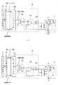
【0016】
このバッテリ充放電装置1には、100V(ボルト)又は200Vの電圧の単相三線方式交流電源(以下「交流電源」と称す。)60から、12Vの定格出力電圧でかつ40A(アンペア)の最大出力電流の電力を生成し出力する直流電源回路2を備えている。この直流電源回路2で生成された直流電流は、充電スイッチング回路4へ供給され、バッテリ61の充電電流として使用される。なお、直流電源回路2は、上記した充電電流を生成する一方で、制御ユニット3を駆動させるための駆動電圧をも生成し出力しているが、その説明および図示は省略している。また、直流電源回路2のグランド側端子Nは接地されている。
【0017】
充電スイッチング回路4は、直流電源回路2からバッテリ61へ供給される充電電流の通電をオン又はオフするための回路であり、制御電圧により動作される電圧制御型スイッチング素子である絶縁ゲート型バイポーラトランジスタ(以下単に「トランジスタ」と称す。)IGBT1と、ツェナー電圧が15VのツェナーダイオードZD1,ZD2と、10kΩの抵抗R1と、非充電型スナバ回路5とを備えている。トランジスタIGBT1のコレクタ端子(電圧制御型スイッチング素子の入力端)は、直流電源回路2のプラス側出力端Pと接続されるとともに、非充電型スナバ回路5を介してトランジスタIGBT1のエミッタ端子(電圧制御型スイッチング素子の出力端)に接続されている。
【0018】
また、トランジスタIGBT1のゲート端子(電圧制御型スイッチング素子の制御端)にはツェナーダイオードZD1のアノード端子が、そのツェナーダイオードZD1のカソード端子にはツェナーダイオードZD2のカソード端子が、そのツェナーダイオードZD2のアノード端子にはトランジスタIGBT1のエミッタ端子が、それぞれ接続されている。この接続によって、トランジスタIGBT1がオンオフされる際に、ゲート・エミッタ端子間に生じるサージ電圧などの過電圧を抑制して、かかる過電圧からトランジスタIGBT1を保護することができる。
【0019】
トランジスタIGBT1のゲート・エミッタ端子間には、保護およびゲート電圧のフローティング防止用の10kΩの抵抗R1が、ツェナーダイオードZD1,ZD2と並列に挿入されると共に、このトランジスタIGBT1のゲート端子およびエミッタ端子はそれぞれ別々に、制御ユニット3の充電ドライブ回路48と接続されている。なお、充電ドライブ回路48の詳細については後述する。
【0020】
スナバ回路5は、100Ωの抵抗R10と、ダイオードD3と、1μFのコンデンサC2とから構成されている。抵抗R10とダイオードD3とは並列に接続されており、ダイオードD3のアノード端子がトランジスタIGBT1のコレクタ端子と接続されている。ダイオードD3のカソード端子は、抵抗R10と直列接続されるコンデンサC2の一端に接続されており、このコンデンサC2の他端はトランジスタIGBT1のエミッタ端子に接続されている。このスナバ回路5によって、トランジスタIGBT1がオンオフされる際にゲート・エミッタ端子間に生じるサージ電圧などの過電圧を抑制して、かかる過電圧からトランジスタIGBT1を保護することができる。
【0021】
電流電圧変換回路6は、図1に示すように、充電スイッチング回路4から出力される充電電流(トランジスタIGBT1のコレクタ電流)が入力端から出力端へ通電することによって、その充電電流を電圧に変換して、充電ドライブ回路48の電流フィードバック回路48cへ出力するための回路である。この電流電圧変換回路6は、充電スイッチング回路4のトランジスタIGBT1のエミッタ端子と逆流阻止回路7との間に挿入された0.1Ω(75W(ワット))のシャント抵抗R2で構成されている。
【0022】
この電流電圧変換回路6によれば、充電スイッチング回路4からの出力された充電電流(トランジスタIGBT1のコレクタ電流)は、シャント抵抗R2によって、その電流値を1/10倍した電圧値に変換され、充電ドライブ回路48の電流フィードバック回路48cへ出力される。例えば、充電電流値が30Aである場合には、電流電圧変換回路6は3Vの出力電圧を電流フィードバック回路48cへ出力する。
【0023】
逆流阻止回路7は、充電スイッチング回路4から出力された充電電流やバッテリ61からの放電電流が充電スイッチング回路4へ逆流することを阻止するための回路であり、平均整流電流が30Aで且つピーク繰返し逆電圧が40Vのショットキーバリア整流素子である一対のダイオードD1,D2で構成されている。このダイオードD1,D2は、そのアノード端子が電流電圧変換回路6の出力端にそれぞれ接続されるとともに、そのカソード端子同士が接続されている。
【0024】
継電回路8は、バッテリ61の正極端子61aの接続先を、充電スイッチング回路4側又は放電スイッチング回路12側のいずれか一方に切り換えると共に、バッテリ充放電装置1の停止時にスイッチング回路4,5とバッテリ61の正極端子61aとを絶縁するための回路である。この継電回路8は、後述する充電動作コイル29によりオン又はオフされる有接点方式の充電系リレースイッチSW1と、放電動作コイル30によりオン又はオフされる有接点方式の放電系リレースイッチSW2とから構成されている。
【0025】
充電系リレースイッチSW1の入力端は、逆流阻止回路7の出力端(即ち、ダイオードD1,D2のカソード端子)に接続される一方、充電系リレースイッチSW1の出力端は、負荷回路9及び電流電圧検出回路10と接続されている。また、放電系リレースイッチSW2の入力端は、逆流阻止回路7の出力端に接続される一方、放電系リレースイッチSW2の出力端は、放電回路R3と接続されている。なお、充電系リレースイッチSW1及び放電系リレースイッチSW2は、その初期状態においてオフ(切断)状態とされている。
【0026】
負荷回路9は、継電回路8のリレースイッチSW1,SW2の双方がオフ状態の場合にバッテリ61の正極端子61a及び負極端子61b間の電圧(即ち、端子電圧)を検出するための負荷となるRC直列回路であり、接続プラグ15のプラス側端子15aとマイナス側端子15bとの間に設けられている。負荷回路9は、100Ω(3W)の抵抗R3と、1μF(250V)のコンデンサC1とから構成されており、抵抗R3の一端が充電系リレースイッチSW1の出力端と電流電圧検出回路10に接続され、抵抗R3の他端がコンデンサC3の一端に接続され、コンデンサC3の他端が接続プラグ15のマイナス側端子15bに接続されている。また、接続プラグ15のマイナス側端子15bは、直流電源回路2のグランド側出力端Nとも接続されている。
【0027】
電流電圧検出回路10は、バッテリ61の正極端子61aを通過する電流とバッテリ61の正極端子61aへ印加される電圧とを検出するための回路であり、0.02Ω(50W)の抵抗R4で構成されている。この抵抗R4は、その一端が接続プラグ15のプラス側端子15aに接続されており、その他端が負荷回路9の抵抗R3の一端及び充電系リレースイッチSW1の出力端に接続されている。バッテリ61の正極端子61aへ向けて(又は正極端子61aから)流れる電流が抵抗R4を通過すると、抵抗R4の両端で電圧降下が生じる。よって、この電圧降下量を電流電圧測定回路50で検出すれば、抵抗R4の抵抗値に基づいてオームの法則から抵抗R4を通過した電流値を測定できる。また、抵抗R4における接続プラグ15のプラス側端子15a側端の電圧は、バッテリ61の正極端子61aの端子電圧として電流電圧測定回路50により検出される。
【0028】
具体的に、バッテリ61の正極端子61aを通過する電流とは、充電時にバッテリ61へ正極端子61aへ流入する充電電流と、放電時にバッテリ61から流出する放電電流であり、バッテリ61の正極端子61aへ印加される電圧とは、充電時に正極端子61aへ印加される充電電圧と、放電時に正極端子61aへ印加される放電電圧と、充電系リレースイッチSW1のオフ状態にバッテリ61の正極端子61aから負荷回路9へ印加される電圧であるバッテリ端子電圧とである。
【0029】
放電回路11は、バッテリ61を放電させる場合の負荷用の回路であり、0.22Ω(100W)の抵抗R5,R6が並列接続されて構成されている。この抵抗R5,R6の一端は放電系リレースイッチSW2の出力端にまとめて接続されており、抵抗R5,R6の他端は放電スイッチング回路12にまとめて接続されている。継電回路8の両リレースイッチSW1,SW2がオン状態となり、更に、放電スイッチング回路12がオン状態となると、バッテリ61から流出する放電電流が放電回路11を通過して、バッテリ61の電力が消費されるのである。
【0030】
放電スイッチング回路12は、バッテリ61から流出する放電電流の通電をオン又はオフするための回路であり、トランジスタIGBT1と同種の電圧制御型スイッチング素子であるトランジスタIGBT2と、ツェナー電圧が15VのツェナーダイオードZD3,ZD4と、10kΩの抵抗R7と、非充電型スナバ回路13とを備えている。この放電スイッチング回路12によれば、トランジスタIGBT2のゲート端子およびエミッタ端子はそれぞれ別々に、制御ユニット3の放電ドライブ回路49と接続されている。スナバ回路13は、100Ωの抵抗R12と、ダイオードD4と、1μFのコンデンサC3とから構成されている。
【0031】
なお、放電スイッチング回路12におけるトランジスタIGBT2、ツェナーダイオードZD3,ZD4及び抵抗R7のその他の接続状態は、上記した充電スイッチング回路4におけるトランジスタIGBT1、ツェナーダイオードZD1,ZD2及び抵抗R1の接続状態と同一であるので、その説明を省略する。また、スナバ回路13における抵抗R12、ダイオードD4及びコンデンサC3の接続状態は、スナバ回路5における抵抗R10、ダイオードD3及びコンデンサC2の接続状態と同一であるのでその説明を省略する。
【0032】
電流電圧変換回路14は、図1に示すように、放電スイッチング回路12から出力される放電電流、即ち、トランジスタIGBT2のコレクタ電流を電圧に変換し、放電ドライブ回路49の電流フィードバック回路49cへ出力するための回路である。この電流電圧変換回路14は、放電スイッチング回路12のトランジスタIGBT2のエミッタ端子と接続プラグ15のマイナス側端子15bとの間に挿入された0.1Ω(75W(ワット))のシャント抵抗R8で構成されている。この電流電圧変換回路14によれば、放電スイッチング回路12からの出力された放電電流は、シャント抗R8によって、その電流値を1/10倍した電圧値に変換され、放電ドライブ回路49の電流フィードバック回路48cへ出力される。
【0033】
次に、図1及び図2を参照して、制御ユニット3について説明する。制御ユニット3には、CPU21、EEPROM22、RAM23、タイマ回路24、A/D変換器25、D/A変換器26が設けられており、これらのCPU21、EEPROM22、RAM23、タイマ回路24、A/D変換器25、D/A変換器26は、アドレスバス及びデータバスで構成されたバスライン27を介して相互に接続されている。
【0034】
バスライン27は、また、入出力ポート28にも接続されており、この入出力ポート28には、充電動作コイル29、放電動作コイル30、スタートボタン31、ストップボタン32、リセットボタン33、非常停止ボタン34、再生前処理ボタン35、小容量処理ボタン36、中容量処理ボタン37、大容量処理ボタン38、ブザー39、液晶ディスプレイ(LCD)40、スタートランプ41、ストップランプ42、リセットランプ43、再生前処理ランプ44、小容量処理ランプ45、中容量処理ランプ46、大容量処理ランプ47、充電ドライブ回路48、放電ドライブ回路49、電流電圧測定回路50が接続されている。
【0035】
CPU21は、EEPROM22に記憶される各種のプログラムを実行する演算装置である。EEPROM22は、書き換え可能な不揮発性メモリであり、このバッテリ充放電装置1で実行される制御プログラム22aなどを格納している。このEEPROM22に記憶されたデータは、バッテリ充放電装置1の電源オフ後も保持される。また、図4〜図9に示すフローチャートのプログラムは、制御プログラム22aの一部としてEEPROM22内に記憶されている。タイマ回路24は時間の計時を行うためのものであり、タイマ回路24により計時された時間はCPU21によって読み出され、各処理に使用される。
【0036】
A/D変換器25は、電流電圧測定回路50から入力されるアナログの電圧値(電圧データ)をデジタルの10ビットの数値データに変換して出力するものである。一方、D/A変換器26は、CPU21により演算された8ビットのデジタル数値データをアナログの電圧データに変換し、充電ドライブ回路48又は放電ドライブ回路49へ出力するものである。このD/A変換器26から出力される電圧データには、図7のバッテリ放電処理において放電ドライブ回路49へ入力される放電ドライブ指令および放電制御指令と、図8のバッテリ充電処理において充電ドライブ回路48へ入力される充電ドライブ指令および充電制御指令とがある。
【0037】
RAM23は、バッテリ充放電装置1の各動作の実行時に各種のデータを一時的に記憶するための揮発性メモリであり、処理モードメモリ23aと、最低充電時間カウンタ23bと、単位処理時間カウンタ23cと、充電回数カウンタ23dと、放電回数カウンタ23eと、端子電圧メモリ23fと、放電前電圧メモリ23gと、パルス電圧メモリ23hと、ベース電圧メモリ23iと、放電完了フラグ23jと、強制終了フラグ23kとを備えている。
【0038】
処理モードメモリ23aは、選択されている処理モードを記憶するためのメモリである。ここで、処理モードとは、バッテリ61へ施される処理種別であり、再生前処理モード、小容量処理モード、中容量処理モード、及び、大容量処理モードの4種類がある。再生前処理モードは、バッテリ61が著しく劣化している場合に他の3種類の処理モードに前置される処理モードであり、再生前処理モードが選択される場合、処理モードメモリ23aには「0」が記憶される。小容量処理モードは、小容量のバッテリ61を充電する場合の処理モードであり、小容量処理モードが選択される場合、処理モードメモリ23aには「1」が記憶される。中容量処理モードは、中容量のバッテリ61を充電する場合の処理モードであり、中容量処理モードが選択される場合、処理モードメモリ23aには「2」が記憶される。大容量処理モードは、大容量のバッテリ61を充電する場合の処理モードであり、大容量処理モードが選択される場合、処理モードメモリ23aには「3」が記憶される。
【0039】
このように処理モードメモリ23aには、選択されている処理モードに応じて「0」〜「3」のいずれかの値が記憶される。これらの4種類の処理モードの選択は、再生前処理ボタン35、小容量処理ボタン36、中容量処理ボタン37、又は、大容量処理ボタン38のいずれかが押下されることによって行われる。なお、再生前処理ランプ44、小容量処理ランプ45、中容量処理ランプ46、及び、大容量処理ランプ47は、使用者により押下された処理ボタン35〜37に対応するものが点灯される。
【0040】
ここで、自動車用鉛蓄電池であるバッテリ61には日本工業規格(JIS D 5301)に準拠した複数の形式があり、この形式に応じて容量がほぼ決定される。具体的に、バッテリ61の容量には、上記規格に準拠したバッテリの幅及び高さに応じて7種類の区分A,B,D,E,F,G,Hがあり、区分Aのバッテリ61の容量が最も小さく、以降、BからHの順に容量が大きくなる。本実施例では、区分A,Bのバッテリ61が小容量処理モードで、区分D,E,Fのバッテリ61が中容量処理モードで、区分G,Hのバッテリが大容量処理モードで処理される。
【0041】
最低充電時間カウンタ23bは、図7のバッテリ充電処理を繰り返し実行する最低時間(最低充電時間)を記憶するためのカウンタであり、本実施例では1時間に相当する値に設定される。よって、図7のバッテリ充電処理は、最低充電時間カウンタ23bの値分の時間、即ち、本実施例では少なくとも1時間は繰り返し実行されるのである。
【0042】
単位処理時間カウンタ23cは、1回当たりのバッテリ再生前処理(図5参照)やバッテリ充電処理(図8参照)においてバッテリ61へ実際に電流を流入させ続ける時間(実充電継続時間)、及び、1回当たりのバッテリ放電処理(図7参照)においてバッテリ61から電流を実際に流出させ続ける時間(実放電継続時間)、に相当する値を記憶するためのカウンタである。この単位処理時間カウンタ23cの初期値は、選択された処理モード毎に所定値に設定される。
【0043】
例えば、本実施例では、処理モードメモリ23aに「0」が記憶され再生前処理モードが選択されている場合、単位処理時間カウンタ23cには初期値として30分の実充電継続時間に相当する値が設定される。また、処理モードメモリ23aに「1」又は「2」が記憶され小容量処理モード又は中容量処理モードが選択されている場合にあっては、5分の実充電継続時間(又は、実放電継続時間)に相当する値が、単位処理時間カウンタ23cの初期値として設定される。更に、処理モードメモリ23aに「3」が記憶され大容量処理モードが選択されている場合にあっては、8分の実充電継続時間(又は、実放電継続時間)に相当する値が、単位処理時間カウンタ23cの初期値として設定される。
【0044】
充電回数カウンタ23dは、図6のバッテリ再生充放電処理において、図8に示すバッテリ充電処理を繰り返し実行可能な最大回数を記憶するためのカウンタであり、そのカウンタ23dの初期値は、小容量処理モード、中容量処理モード又は大容量処理モード毎に所定値に設定される。ここで、図6のバッテリ再生充放電処理では、図8のバッテリ充電処理が繰り返し実行される時間を8時間程度に制限している。
【0045】
例えば、図8のバッテリ充電処理では、小容量処理モード又は中容量処理モードの場合に実充電継続時間が5分であり、その実充電継続時間の経過後に3分のインターバル時間を設けているので、1回当たりのバッテリ充電処理の実行時間は約8分となる。この1回当たりのバッテリ充電処理の実行時間である約8分で8時間(480分)を除算すると、60になる。よって、小容量処理モード及び中容量処理モードの場合には、8時間に相当する充電回数カウンタ23dの初期値として60が設定される。
【0046】
また、大容量処理モードの場合にあっては実充電継続時間が8分であり、その実充電継続時間の経過後に3分のインターバル時間を設けているので、1回当たりのバッテリ充電処理の実行時間は約11分となる。この1回当たりのバッテリ充電処理の実行時間である約11分で8時間(480分)を除算すると、約44になる。よって、大容量処理モードの場合には、8時間に相当する充電回数カウンタ23dの初期値として44が設定される。
【0047】
放電回数カウンタ23eは、図6のバッテリ再生充放電処理において図7に示すバッテリ放電処理を連続して繰り返し実行可能な最大回数を記憶するためのカウンタであり、そのカウンタ23eの初期値には、小容量処理モードの場合に5回が、中容量処理モードの場合に8回が、大容量処理モードの場合に10回が、それぞれ設定される。即ち、図7のバッテリ放電処理を連続して繰り返す場合には、放電回数カウンタ23eの値(図7のバッテリ放電処理の最大実行回数)分しか行われないのである。
【0048】
端子電圧メモリ23fは、電流電圧測定回路50から出力されるバッテリ61の端子電圧値を一時的に記憶するためのメモリである。バッテリ61の正極端子61aの電圧(端子電圧)は、電流電圧測定回路50へ入力され、この電流電圧測定回路50によって、後述するA/D変換器25の入力レベルに対応するアナログの電圧値(電圧データ)に変換される。この変換された電圧データは、入出力ポート28を介してA/D変換器25へ入力され、このA/D変換器25によりデジタルの10ビットの数値データに変換され、端子電圧メモリ23fへ記憶される。即ち、端子電圧メモリ23fの値は、バッテリ61の端子電圧値に対応する10ビットの数値データとして記憶されるのである。
【0049】
放電前電圧メモリ23gは、図7のバッテリ放電処理の実行前に端子電圧メモリ23fの値を保存するメモリである。即ち、この放電前電圧メモリ23gには、バッテリ61から電流が流出し放電される以前の端子電圧に相当する値である10ビットのデジタル数値データが記憶される。
【0050】
パルス電圧メモリ23hは、図8のバッテリ充電処理において、バッテリ61へ充電電流としてパルス充電電流が流入される時間(パルス出力時間)中に、バッテリ61に印加されている電圧(パルス電圧)値を記憶するためのメモリである。バッテリ61の正極端子61aへ印加されるパルス電圧は、上記した端子電圧メモリ23fの場合と同様に、電流電圧測定回路50、入出力ポート28及びA/D変換器25を介してデジタルの10ビットの数値データに変換されて、パルス電圧メモリ23hへ記憶される。
【0051】
ベース電圧メモリ23iは、図8のバッテリ充電処理において、バッテリ61へ充電電流としてベース充電電流が流入される時間(ベース出力時間)中に、バッテリ61に印加されている電圧(ベース電圧)値を記憶するためのメモリである。バッテリ61の正極端子61aへ印加されるベース電圧は、パルス電圧メモリ23hの場合と同様に、電流電圧測定回路50、入出力ポート28及びA/D変換器25を介してデジタルの10ビットの数値データに変換されて、ベース電圧メモリ23iへ記憶される。
【0052】
放電完了フラグ23jは、図6のバッテリ再生充放電処理において、バッテリ61に対して図7のバッテリ放電処理を実行する必要があるか否かを示すフラグである。放電完了フラグ23jがオンの場合には、バッテリ61に対して図7のバッテリ放電処理をこれ以上実行する必要がなく、オフの場合にはバッテリ61に対して図7のバッテリ放電処理を実行する必要があること示すものである。放電完了フラグ23jは、バッテリ放電処理の実行前後のバッテリ61の端子電圧の差が所定値未満である場合にオン状態にセットされる(図6のS52)一方、RAM23が初期化される場合(図4のS1)、パルス電圧メモリ23hの値が35Vに相当する値以上の場合、及び、ベース電圧メモリ23iの値が14.5Vに相当する値以上の場合(図6のS63)にオフ状態にリセットされる。
【0053】
強制終了フラグ23kは、図7のバッテリ放電処理において、図6のバッテリ再生充放電処理を強制終了させる必要があるか否かを示すフラグである。この強制終了フラグ23kは、そのRAM23の初期化によりオフ状態に設定されており、図9(b)の放電電圧測定処理で測定されたバッテリ61の端子電圧が10.5V以下になった場合にオン状態に変更される。放電中のバッテリ61が10.5V以下の端子電圧となった場合、そのバッテリ61は放電終止電圧に達しており、それ以上の放電はバッテリ61を過放電状態にしてしまう。そのため、かかる強制終了フラグ23kをオンして、図6のバッテリ再生充放電処理を強制終了させるのである。
【0054】
充電動作コイル29は、その充電動作コイル29が通電状態にあるか否かに応じて充電系リレースイッチSW1をオン又はオフするためのものであり、通電状態の場合に充電系リレースイッチSW1をオン状態にする一方、通電停止状態の場合に充電系リレースイッチSW1をオフ状態にする。また、放電動作コイル30は、その放電動作コイル30が通電状態にあるか否かに応じて放電系リレースイッチSW2をオン又はオフするためのものであり、通電状態の場合に放電系リレースイッチSW2をオン状態にする一方、通電停止状態の場合に放電系リレースイッチSW2をオフ状態にする。
【0055】
スタートボタン31は、図5のバッテリ再生前処理および図6のバッテリ再生充放電処理の開始時に使用者により押下されるものであり、この押下によって上記各処理が開始されると共にスタートランプ41が点灯される。ストップボタン32は、図5のバッテリ再生前処理および図6のバッテリ再生充放電処理の停止時に使用者により押下されるものであり、この押下によって上記各処理が停止されると共にストップランプ42が点灯される。リセットボタン33は、RAM23、各種ランプ41〜49、ブザー39及びLCD40を初期化する際に使用者により押下されるものであり、このリセットボタン33の押下を使用者へ促すためにリセットランプ43が点灯される。
【0056】
非常停止ボタン34は、バッテリ充放電装置1が稼動している場合に強制的に稼動を停止するために使用者により押下されるものであり、この非常停止ボタン34が押下されると、直流電源回路2内に設けられたリレースイッチ(図示せず)が作動して、交流電源60側と充電スイッチング回路4側との接続状態が切断される。
【0057】
図2を参照して、充電ドライブ回路48及び放電ドライブ回路49について説明する。図2(a)は、充電ドライブ回路48の構成を概略的に表した図であり、図2(b)は、放電ドライブ回路49の構成を概略的に表した図である。なお、図2(b)に示すように放電ドライブ回路49は、図2(a)に示した充電ドライブ回路48と同一の構成とされている。
【0058】
図2(a)に示すように、充電ドライブ回路48は、指令電圧生成回路48aと、絶縁回路48bと、電流フィードバック回路48cとを、ゲート抵抗回路48dとを備えている。指令電圧生成回路48aは、入出力ポート28を介してD/A変換器26から入力されるアナログの電圧である充電ドライブ指令および充電制御指令から充電指令電圧を生成して出力する回路である。
【0059】
この指令電圧生成回路48aの第1入力端IN1には、D/A変換器26から入出力ポート28を介して出力される充電ドライブ指令が入力され、指令電圧生成回路48aの第2入力端IN2には、D/A変換器26から入出力ポート28を介して出力される充電制御指令が入力される。指令電圧生成回路48aへ入力された充電ドライブ指令及び充電制御指令は、それぞれ指令電圧生成回路48a内の電圧ホロワ(図示せず)を介して、指令電圧生成回路48a内の差動増幅回路(図示せず)へ入力される。この指令電圧生成回路48aの差動増幅回路は、充電ドライブ指令及び充電制御指令の電圧差を充電指令電圧として指令電圧生成回路48aの出力端OUTから絶縁回路48bへ出力する。
【0060】
絶縁回路48bは、指令電圧生成回路48a側の入力段と、電流フィードバック回路48c側の出力段とを絶縁するための絶縁アンプ(アイソレーションアンプ)ISO1で構成されている。この絶縁回路48bの絶縁アンプISO1の入力端へ入力された充電指令電圧は、その絶縁アンプISO1の出力端から電流フィードバック回路48cへ出力される。
【0061】
電流フィードバック回路48cは、絶縁回路48bから入力される充電指令電圧と電流電圧変換回路6の出力電圧との偏差を0Vへ収束させるための帰還演算回路であり、オペアンプOP1で構成されている。このオペアンプOP1の非反転入力端は絶縁回路48bの出力端と接続されており、その反転入力端は電流電圧変換回路6のシャント抵抗R2とトランジスタIGBT1のエミッタ端子との間に接続されている。オペアンプOP1の出力端は、10Ωの抵抗R9で構成されたゲート抵抗回路48dと接続されており、このゲート抵抗回路48dを介してトランジスタIGBT1のゲート端子に接続されている。
【0062】
図2(b)に示すように、放電ドライブ回路49は、図2(a)に示した充電ドライブ回路48と同様に、指令電圧生成回路49aと、絶縁回路49bと、電流フィードバック回路49cとを、ゲート抵抗回路49dとを備えている。指令電圧生成回路49aは、入出力ポート28を介してD/A変換器26から入力されるアナログの電圧である放電ドライブ指令および放電制御指令から放電指令電圧を生成して出力する回路である。この指令電圧生成回路49aの第1入力端IN1には、D/A変換器26から入出力ポート28を介して出力される放電ドライブ指令が入力され、指令電圧生成回路49aの第2入力端IN2には、D/A変換器26から入出力ポート28を介して出力される放電制御指令が入力され、この充電ドライブ指令及び充電制御指令の電圧差を放電指令電圧として指令電圧生成回路49aの出力端OUTから絶縁回路49bへ出力している。
【0063】
絶縁回路49bの絶縁アンプISO2の入力端へ入力された放電指令電圧は、その絶縁アンプISO2の出力端から電流フィードバック回路49cへ出力され、電流フィードバック回路49cのオペアンプOP2の非反転入力端へ入力される。また、オペアンプOP2の反転入力端は電流電圧変換回路14のシャント抵抗R8とトランジスタIGBT2のエミッタ端子との間に接続されている。更に、オペアンプOP2の出力端は、10Ωの抵抗R11で構成されたゲート抵抗回路49dと接続されており、このゲート抵抗回路49dを介してトランジスタIGBT2のゲート端子に接続されている。
【0064】
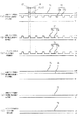
図3を参照して、充電ドライブ回路48及び放電ドライブ回路49の動作について説明する。図3(a)は、充電ドライブ回路48の指令電圧生成回路48aへの入力電圧波形を示した図であり、図3(b)は、指令電圧生成回路48aの出力電圧波形を示した図であり、図3(c)は、充電スイッチング回路4のトランジスタIGBT1のコレクタ電流、即ち、バッテリ61への充電電流波形を示した図である。なお、図3(a)〜(c)では、中容量処理モードが選択された場合の各波形を示している。
【0065】
まず、バッテリ充電処理において、D/A変換器26は、入出力ポート28を介して3Vの充電ドライブ指令71を充電ドライブ回路48の指令電圧生成回路48aの第1入力端IN1へ出力すると共に、入出力ポート28を介して充電制御指令72を充電ドライブ回路48の指令電圧生成回路48aの第2入力端IN2へ出力する(図3(a))。ここで、充電制御指令72は、1.5Vのパルス制御指令72aと、2.2Vのベース制御指令72bとを交互に繰り返したものである。
【0066】
なお、パルス制御指令72aは、小容量処理モードの場合に2.2V、大容量処理モードの場合に0.5V、及び、再生前処理モードの場合に1.5Vに設定される。また、ベース制御指令72bは、小容量処理モードの場合に2.7V、大容量処理モードの場合に2.0V、及び、再生前処理モードの場合に2.8Vに設定される。
【0067】
ここで、本実施例のパルス制御指令72aは、その周波数が2kHzで且つデューティ比が25%に設定されており、結果、パルス制御指令72aの周期t1が500μsとされると共に、1周期t1当たりの出力時間(パルス出力時間)t2は125μsとされる。一方、ベース指令制御72bは、その周波数が2kHzで且つデューティ比が75%に設定されており、結果、ベース制御指令72bの周期t3が500μsとされると共に、1周期t3当たりの出力時間(ベース出力時間)t4は375μsとされる。
【0068】
指令電圧生成回路48aは、第1及び第2入力端IN1,IN2へ入力された充電ドライブ指令71から充電制御指令72を減算した電圧を充電指令電圧73として出力する(図3(b))。この充電指令電圧73は、1.5Vのパルス充電指令電圧73aと、0.8Vのベース充電指令電圧73bとを交互に繰り返したものである。具体的に、充電指令電圧73は、パルス充電指令電圧73aが125μsのパルス出力時間t2だけ保持された後、ベース充電指令電圧73bが375μsのベース出力時間t4だけ保持されている。
【0069】
なお、パルス充電指令電圧73aは、小容量処理モードの場合に0.8V、大容量処理モードの場合に2.5V、及び、再生前処理モードの場合に0.2Vとなる。また、ベース充電指令電圧73bは、小容量処理モードの場合に0.3V、大容量処理モードの場合に1.0V、及び、再生前処理モードの場合に1.5Vとなる。
【0070】
充電指令電圧73は、絶縁回路48bを介して電流フィードバック回路48cへ入力され、この電流フィードバック回路48cによって、充電スイッチング回路4のトランジスタIGBT1のゲート端子へ印加されるべきゲート電圧に変換される。このゲート電圧は、ゲート抵抗回路48dへ入力され、このゲート抵抗回路48dの抵抗R9によってゲート電流に変換され、トランジスタIGBT1のゲート端子へ流入する。このゲート電圧及びゲート電流がゲート端子へ印加されると、トランジスタIGBT1がオンされて、トランジスタIGBT1のコレクタ・エミッタ端子間にコレクタ電流(充電電流)74が流れる(図3(c))。
【0071】
充電電流74は、15Aのパルス充電電流(パルス電流成分)74aと、8Vのベース充電電流(ベース電流成分)74bとを交互に繰り返したものである。具体的に、充電電流74は、パルス充電電流74aが125μsのパルス出力時間t2だけ保持された後、ベース充電電流74bが375μsのベース出力時間t4だけ保持されている。このように略一定のベース充電電流74bに略矩形波状に変化する大電流のパルス充電電流74aを重畳させた充電電流74によれば、バッテリ61の正極端子61aへ流入された場合に、大電流のパルス充電電流74aによりバッテリ61の電極表面に析出したサルフェーションが分解除去される。しかも、パルス出力時間t2の経過後は、ベース充電電流74bがバッテリ61へ流入されるので、かかるベース充電電流74bによりバッテリ61を充電することができ、更に、パルス充電電流74aによりバッテリ61の充電速度を加速させることができるのである。
【0072】
なお、パルス充電電流74aは、小容量処理モードの場合に8A、大容量処理モードの場合に25A、及び、再生前処理モードの場合に2Aとなる。また、ベース充電電流74bは、小容量処理モードの場合に3A、大容量処理モードの場合に10A、及び、再生前処理モードの場合に15Aとなる。
【0073】
図3(d)は、放電ドライブ回路49の指令電圧生成回路49aへの入力電圧波形を示した図であり、図3(e)は、指令電圧生成回路49aの出力電圧波形を示した図であり、図3(f)は、放電スイッチング回路12のトランジスタIGBT2のコレクタ電流、即ち、バッテリ61からの放電電流波形を示した図である。なお、図3(a)〜(c)では、中容量処理モードが選択された場合の各波形を示している。
【0074】
まず、バッテリ放電処理において、D/A変換器26は、入出力ポート28を介して、3Vの放電ドライブ指令75を放電ドライブ回路49の指令電圧生成回路49aの第1入力端IN1へ出力すると共に、2.2Vの放電制御指令76を指令電圧生成回路49aの第2入力端IN2へ出力する(図3(d))。指令電圧生成回路49aは、第1及び第2入力端IN1,IN2へ入力された放電ドライブ指令75から放電制御指令76を減算した0.8Vの放電指令電圧77を生成して出力する(図3(e))。
【0075】
なお、放電制御指令76は、小容量処理モードの場合に2.7V、大容量処理モードの場合に2.0Vに設定され、放電指令電圧77は、小容量処理モードの場合に0.3V、大容量処理モードの場合に1.0Vで指令電圧生成回路49aから出力される。
【0076】
放電指令電圧77は、絶縁回路49bを介して電流フィードバック回路49cへ入力され、この電流フィードバック回路49cによって、放電スイッチング回路14のトランジスタIGBT2のゲート端子へ印加されるべきゲート電圧に変換される。このゲート電圧は、ゲート抵抗回路49dへ入力され、このゲート抵抗回路49dの抵抗R11によってゲート電流に変換され、トランジスタIGBT2のゲート端子へ流入する。
【0077】
このゲート電圧及びゲート電流がゲート端子へ印加されると、トランジスタIGBT2がオンされて、バッテリ61から放電回路11を経由して、トランジスタIGBT2のコレクタ・エミッタ端子間に8Aのコレクタ電流(放電電流)78が流れる(図3(f))。なお、放電電流78は、小容量処理モードの場合に3A、大容量処理モードの場合に10Aに調整される。
【0078】
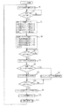
次に、図4から図9のフローチャートを参照して、上記のように構成されたバッテリ充放電装置1の動作について説明する。図4は、バッテリ充放電装置1のメイン処理を示したフローチャートである。このメイン処理は、バッテリ充放電装置1の電源スイッチがオンされた場合に実行される処理である。この処理では、まず、RAM23の値が初期化され、処理ボタン35〜38のいずれかが押下されるまで待機する(S2:No)。
【0079】
使用者により処理ボタン35〜38のいずれかが押下されると(S2:Yes)、再生前処理ボタン35の場合は「0」を、小容量処理ボタン36の場合は「1」を、中容量処理ボタン37の場合は「2」を、大容量処理ボタン38の場合は「3」を、処理モードメモリ23aへ書き込む(S3)。また、処理モードメモリ23aの値が「0」の場合は再生前処理ランプ44を、処理モードメモリ23aの値が「1」の場合は小容量処理ランプ45を、処理モードメモリ23aの値が「2」の場合は中容量処理ランプ46を、処理モードメモリ23aの値が「3」の場合は大容量処理ランプ47を点灯する(S4)。
【0080】
処理ランプ44〜47の点灯後、スタートボタン31が押下されるまで待機し(S5:No)、それが押下されると(S5:Yes)、スタートランプ41を点灯して(S6)、処理モードメモリ23aの値を再び判断する(S7)。処理モードメモリ23aの値が「0」の場合は(S7:「0」)、バッテリ再生前処理を実行し(S8)、処理モードメモリ23aの値がその他の場合は(S7:「1,2,3」)、バッテリ再生充放電処理を実行する(S9)。S8及びS9の処理後は、リセットボタン43が押下されるまで待機し(S10:No)、それが押下されると(S10:Yes)、全てのランプ41〜47やブザー39のうち作動しているものを停止し(S11)、LCD40を初期化して(S12)、他の処理を実行した後(S13)、処理をS1へ移行する。その後はS1からS13までの処理を電源がオフされるまで繰り返す。
【0081】
図5は、バッテリ再生前処理を示したフローチャートである。このバッテリ再生前処理は、主に、バッテリ61の電極表面に析出したサルフェーションにより電解液の比重が大幅に低下し、その劣化度が大幅に悪化したバッテリ61に対して、図6のバッテリ再生充放電処理のバッテリ61の前処理として施される処理である。即ち、このバッテリ再生前処理は、図6のバッテリ再生充放電処理のみでは、バッテリ61のサルフェーションを除去して容量を回復しきれない場合に実行される特別な処理である。
【0082】
バッテリ再生前処理では、まず、単位処理時間カウンタ23cへ30分に相当するカウンタ値を書き込んだ後(S21)、バッテリ61の端子電圧を測定して、その測定した端子電圧を端子電圧メモリ23fへ書き込む(S22)。この端子電圧メモリ23fへ書き込まれた値が1V以上の場合には(S23:Yes)、バッテリ61の正極端子61aが接続プラグ15のプラス側端子15aに接続され且つバッテリ61の負極端子61bが接続プラグ15のマイナス側端子15bに正常に接続されているので、充電動作コイル29へ通電することにより(S24)、充電系リレースイッチSW1をオンして、充電スイッチング回路4から、逆流阻止回路7及びバッテリ61へ至る回路を接続する。
【0083】
S24の通電後、単位処理時間カウンタ23cへ記憶されている値分、即ち、30分の計時を開始し(S25)、タイマ回路24の時間を監視しつつ、3Vの充電ドライブ指令の出力を開始し(S26)、1.5Vの充電制御指令の出力を開始する(S27)。この1.5Vの充電制御指令の出力は125μsのパルス出力時間t2だけ継続され(S28:No)、このパルス出力時間t2が経過すると(S28:Yes)、充電制御指令は2.8Vに切り換えられて出力される(S29)。
【0084】
また、この2.8Vの充電制御指令は375μsのベース出力時間t4だけ継続され(S30:No)、このベース出力時間t4が経過し(S30:Yes)、更に、S25の計時開始から単位処理時間カウンタ23cに記憶されている値分の時間が経過していない場合には(S31:No)、処理をS27へ移行して、S27からS30までの処理を繰り返す。充電ドライブ指令および充電制御指令は充電ドライブ回路48の指令電圧生成回路48cを介して充電指令電圧に変換される。
【0085】
この充電指令電圧は、絶縁回路48bを経た後、電流フィードバック回路48cによって充電スイッチング回路4のトランジスタIGBT1のゲート電圧に変換され、ゲート抵抗回路48dによってトランジスタIGBT1のゲート端子へ流入するゲート電流に変換される。結果、充電スイッチング回路4のトランジスタIGBT1はオンされ、このトランジスタIGBT1を介して直流電源回路2からバッテリ61へ充電電流が流入する。
【0086】
充電電流は、充電スイッチング回路4のトランジスタIGBT1のゲート端子へ印加されるゲート電圧によって調節され、このゲート電圧は、D/A変換器26から出力される充電ドライブ指令及び充電制御指令に応じて決定されている。具体的には充電電流として、2kHzの周波数で且つ25%のデューティ比である15Aのパルス充電電流と、2kHzの周波数で且つ75%のデューティ比である2Aのベース充電電流とが連続して交互にバッテリ61へ30分流入するのである。
【0087】
単位処理時間カウンタ23cに記憶されている値分の計時の終了後は(S31:Yes)、充電ドライブ指令および充電制御指令を0Vにして(S32)、充電スイッチング回路4のトランジスタIGBT1をオフすると共に、充電動作コイル29への通電を停止することにより(S33)、充電系リレースイッチSW1をオフして、バッテリ61への充電電流の流入を停止する。その停止後、3分が経過するまで待機し(S34:No)、この間、バッテリ61は放置されることにより放熱が行われ、バッテリ61の温度上昇が抑制される。
【0088】
S33の処理後から3分が経過すると(S34:Yes)、バッテリ61の端子電圧を測定して端子電圧メモリ23fへ書き込み(S35)、その端子電圧メモリ23fへ書き込まれた内容、即ち、S35の処理で測定されたバッテリ61の端子電圧をLCD40へ表示すると共に、バッテリ再生前処理が正常に終了した旨を示す「正常終了」なる文字をLCD40へ表示して、このバッテリ再生処理を終了する。
【0089】
一方、S23の処理において、端子電圧メモリ23fへ書き込まれた値が1V未満の場合には(S23:No)、バッテリ61の正極端子61aが接続プラグ15のマイナス側端子15bに接続され且つバッテリ61の負極端子61bが接続プラグ15のプラス側端子15aに接続されている。即ち、バッテリ61は接続プラグ15に逆接続されているので、ブザー39を鳴動して、リセットランプ43を点灯すると共に、LCD40へ「バッテリ逆接続」と表示して(S37)、このバッテリ再生前処理を終了する。
【0090】
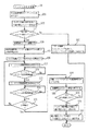
図6は、バッテリ再生充放電処理を示したフローチャートである。このバッテリ再生充放電処理は、バッテリ61の電極表面に析出したサルフェーションを除去することによりバッテリ61の容量を未使用状態に相当する値まで回復させると共に、そのサルフェーション除去処理と並行してバッテリ61を満充電状態まで充電するための処理である。
【0091】
バッテリ再生充放電処理では、まず、最低充電時間カウンタ23bへ1時間に相当するカウンタ値を書き込む(S41)。また、処理モードメモリ23aの値が、「1」又は「2」の場合は60を、「3」の場合は44を、充電回数カウンタ23dへ書き込む(S42)。更に、処理モードメモリ23aの値が、「1」の場合は5を、「2」の場合は8を、「3」の場合は10を、放電回数カウンタ23eへ書き込む(S43)。
【0092】
その後、バッテリ61の端子電圧を測定して、その測定した端子電圧を端子電圧メモリ23fへ書き込む(S44)。この端子電圧メモリ23fへ書き込まれた値が1V以上の場合には(S45:Yes)、バッテリ61が接続プラグ15に正常に接続されているので、更に、端子電圧メモリ23fの値が15Vの放電切換電圧値以上か否かを判断する(S46)。なお、端子電圧メモリ23fの値が1V未満の場合には(S45:No)、バッテリ61が接続プラグ15に逆接続されているので、ブザー39を鳴動して、リセットランプ43を点灯すると共に、LCD40へ「バッテリ逆接続」と表示をして(S66)、このバッテリ再生前処理を終了する。
【0093】
S46の処理において、端子電圧メモリ23fの値が15Vの放電切換電圧値以上の場合には(S46:Yes)、バッテリ61が過充電状態にあるので、バッテリ61に対してバッテリ放電処理を実行する(S47)。図7には、バッテリ放電処理のフローチャートが示されている。
【0094】
図7に示したバッテリ放電処理では、まず、端子電圧メモリ23fの値を放電前電圧メモリ23gへ書き込んで(S71)、バッテリ放電処理(S47)の実行前に測定されたバッテリ61の端子電圧を保持した後、処理モードメモリ23aの値が「1」又は「2」の場合は5分に相当する値を、「3」の場合は8分に相当する値を、単位処理時間カウンタ23cへ書き込んで(S72)、1回当たりのバッテリ放電処理における実放電継続時間を設定する。
【0095】
実放電継続時間の設定後(S72)、充電動作コイル29及び放電動作コイル30の双方へ通電することによって(S73)、充電系リレースイッチSW1及び放電系リレースイッチSW2をオンして、バッテリ61から放電回路11、放電スイッチング回路12に至る回路を接続する。かかる場合、逆流阻止回路7によりバッテリ61からの放電電流が充電スイッチング回路4へ逆流することが防止される。
【0096】
S73の通電後、単位処理時間カウンタ23cへ記憶されている値分の計時を開始し(S74)、タイマ回路24の時間を監視しつつ、3Vの放電ドライブ指令の出力を開始する(S75)。この放電ドライブ指令の出力と共に、処理モードメモリ23aの値が「1」の場合は2.7Vの、「2」の場合は2.2Vの、「3」の場合は2.0Vの放電制御指令の出力を開始して(S76)、単位処理時間カウンタ23cの値分の計時が終了するまで、上記した放電ドライブ指令及び放電制御指令の出力を継続する(S77:No)。
【0097】
放電ドライブ指令および放電制御指令は、放電ドライブ回路49の指令電圧生成回路49aによって、小容量処理モードの場合は0.3Vの、中容量処理モードの場合は0.8Vの、大容量処理モードの場合は1.0Vの放電指令電圧に変換される。この放電指令電圧は、絶縁回路49bを経た後、電流フィードバック回路49cによって放電スイッチング回路12のトランジスタIGBT2のゲート電圧に変換され、ゲート抵抗回路49dによってトランジスタIGBT2のゲート端子へ流入するゲート電流に変換される。結果、放電スイッチング回路12のトランジスタIGBT2はオンされ、小容量モードの場合は3Aの、中容量処理モードの場合は8Aの、大容量処理モードの場合は10Aの放電電流がバッテリ61から放電回路11へ流れて、かかるバッテリ61の放電が行われる。
【0098】
単位処理時間カウンタ23cに記憶されている値分の計時の終了後は(S77:Yes)、放電ドライブ指令および放電制御指令を0Vにして(S78)、放電スイッチング回路12のトランジスタIGBT2をオフすると共に、充電動作コイル29及び放電動作コイル30への通電を停止することにより(S79)、充電系リレースイッチSW1及び放電系リレースイッチSW2をオフして、バッテリ61からの放電電流の流出を停止する。
【0099】
その停止後、強制終了フラグ23kがオンされている場合には(S80:Yes)、「放電終止電圧に達したため強制終了する」とLCD40へ表示して(S81)、図4のメイン処理のS10へ移行することにより(S82)、このバッテリ放電処理が終了し、図4のメイン処理のS10の処理でリセットボタン43が押下されるまで待機する(S10:No)。一方、強制終了フラグ23kがオフの場合には(S80:No)、3分が経過するまで待機する(S83:No)。この間、バッテリ61は放置されることにより放熱が行われ、バッテリ61の過剰な温度上昇が抑制される。
【0100】
S79の処理後から3分が経過すると(S83:Yes)、バッテリ61の端子電圧を測定して端子電圧メモリ23fへ書き込み(S84)、その端子電圧メモリ23fへ書き込まれた内容、即ち、S84の処理で測定されたバッテリ61の端子電圧とLCD40へ表示して(S85)、放電回数カウンタ23eの値から1を減算し(S86)、このバッテリ放電処理を終了して、処理を図6のS48へ移行する。
【0101】
図6に戻って説明する。S48の処理では、端子電圧メモリ23fの値と放電前電圧メモリ23gの値との差を求め(S48)、その差が示す電圧差の値が所定値以上(S49:Yes)、且つ、端子電圧メモリ23fの値が15Vの放電切換電圧値以上の場合には(S50:Yes)、放電回数カウンタ23eの値が0か否かを判断して(S51)、その値が1以上であれば(S51:No)、処理をS47へ移行して、S47からS50の処理を繰り返す。
【0102】
一方、端子電圧メモリ23fの値と放電前電圧メモリ23gの値との差が示す電圧値が所定値未満であれば(S49:No)、放電完了フラグ23jをオンした後に(S52)、バッテリ61に対して充電を施すために処理をS53へ移行する。また同様に、端子電圧メモリ23fの値が15Vの放電切換電圧値未満の場合(S50:No)、放電回数カウンタ23eの値が0の場合(S51:Yes)、更に、上記したS46の処理で端子電圧メモリ23fの値が15Vの放電切換電圧値未満である場合にあっても(S46:No)、処理をS53へ移行する。
【0103】
S53以降の処理では、まず、最低充電時間カウンタ23bへ記憶されている値分の計時が開始されているか否かを判断し(S53)、その計時が未開始であれば(S53:No)、最低充電時間カウンタ23bへ記憶されている値分の計時を開始する(S54)一方、S54の計時が開始されていれば(S53:Yes)、S54の処理をスキップして、バッテリ61に対してバッテリ充電処理を実行する(S55)。図8には、バッテリ充電処理のフローチャートが示されている。
【0104】
図8に示したバッテリ充電処理では、まず、処理モードメモリ23aの値が「1」又は「2」の場合は5分に相当する値を、「3」の場合は8分に相当する値を、単位処理時間カウンタ23cへ書き込んで(S91)、1回当たりのバッテリ充電処理における実充電継続時間を設定し、充電動作コイル29へ通電することによって(S92)、充電系リレースイッチSW1をオンする。結果、充電スイッチング回路4から、逆流阻止回路7及びバッテリ61へ至る回路が接続されるのである。
【0105】
S92の通電後、単位処理時間カウンタ23cへ記憶されている値分の計時を開始し(S93)、タイマ回路24の時間を監視しつつ、3Vの充電ドライブ指令の出力を開始する(S94)。この充電ドライブ指令の出力後、処理モードメモリ23aの値が「1」の場合は2.2Vの、「2」の場合は1.5Vの、「3」の場合は0.5Vの放電制御指令の出力を開始して(S95)、これらの充電ドライブ指令および充電制御指令の出力を、125μsのパルス出力時間t2だけ継続する(S96:No)。
【0106】
パルス出力時間t2が経過すると(S96:Yes)、3Vの充電ドライブ指令の出力は保持されたまま、処理モードメモリ23aの値が「1」の場合は2.7Vの、「2」の場合は2.2Vの、「3」の場合は2.0Vの充電制御指令の出力を開始して(S97)、これらの充電ドライブ指令および充電制御指令の出力を、375μsのベース出力時間t4だけ継続する(S98:No)。
【0107】
ベース出力時間t4が経過し(S98:Yes)、更に、S93の計時開始から単位処理時間カウンタ23cに記憶されている値分の時間が経過していない場合には(S99:No)、3Vの充電ドライブ指令の出力を保持したまま、処理をS95へ移行して、S95からS98までの処理を繰り返す。なお、充電ドライブ指令および充電制御指令による充電ドライブ回路48及び充電スイッチング回路4の動作は、図5のバッテリ再生前処理の場合と同様であり、これらの充電ドライブ指令及び充電制御指令によって、充電スイッチング回路4のトランジスタIGBT1はオンされ、このトランジスタIGBT1を介して直流電源回路2からバッテリ61へ充電電流が流入する。
【0108】
充電電流は、充電スイッチング回路4のトランジスタIGBT1のゲート端子へ印加されるゲート電圧によって調節され、このゲート電圧は、D/A変換器26から出力される充電ドライブ指令及び充電制御指令に応じて決定されている。具体的には充電電流として、2kHzの周波数で且つ25%のデューティ比であるパルス充電電流と、2kHzの周波数で且つ75%のデューティ比であってパルス充電電流より小さなベース充電電流とが交互に途切れることなくバッテリ61へ流入するのである。
【0109】
具体的に、小容量処理モードの場合には8Aのパルス充電電流と3Aのベース充電電流とが5分間、中容量処理モードの場合は15Aのパルス充電電流と8Aのベース充電電流とが5分間、大容量処理モードの場合は5Aのパルス充電電流と10Aのベース充電電流とが8分間、交互に途切れることなくバッテリ61へ充電電流として流入するのである。
【0110】
単位処理時間カウンタ23cに記憶されている値分の計時の終了後は(S99:Yes)、充電ドライブ指令および充電制御指令を0Vにして(S100)、充電スイッチング回路4のトランジスタIGBT1をオフすると共に、充電動作コイル29への通電を停止することにより(S101)、充電系リレースイッチSW1をオフして、バッテリ61への充電電流の流入を停止する。その停止後、3分が経過するまで待機し(S102:No)、この間、バッテリ61は放置されることにより放熱が行われ、バッテリ61の過剰な温度上昇が抑制される。
【0111】
S101の処理後から3分が経過すると(S102:Yes)、バッテリ61の端子電圧を測定して端子電圧メモリ23fへ書き込み(S103)、その端子電圧メモリ23fへ書き込まれた内容、即ち、S103の処理で測定されたバッテリ61の端子電圧をLCD40へ表示して(S104)、充電回数カウンタ23dの値から1を減算し(S105)、このバッテリ充電処理を終了して、処理を図6のS56へ移行する。
【0112】
図6に戻って説明する。バッテリ充電処理の後(S55)、端子電圧メモリ23fの値が13.5Vの充電完了電圧値未満の場合(S56:No)、又は、端子電圧メモリ23fの値が13.5Vの充電完了電圧値以上かつ15Vの放電切換電圧値未満の場合は(S56:Yes,S57:No)、充電回数カウンタ23dの値が0か否かを判断して(S64)、その値が1以上であれば(S64:No)、処理をS53へ移行して、S55からS57までの処理を繰り返し、充電回数カウンタ23dの値が0となれば(S64:Yes)、8時間相当の充電によってもバッテリ61の端子電圧が15Vの放電切換電圧値以上に達していないので、ブザー39を鳴動し、リセットランプ43を点灯し、「電圧不足」とLCD40へ表示して(S65)、このバッテリ再生充放電処理を終了する。
【0113】
一方、S57の処理で、端子電圧メモリ23fの値が15Vの放電切換電圧値以上の場合は(S57:Yes)、放電完了フラグ23jのオンオフを判断し(S58)、放電完了フラグ23jがオフの場合にはS47のバッテリ放電処理へ移行する。一方、放電フラグ23jがオンの場合にはパルス電圧メモリ23h及びベース電圧メモリ23iの値を確認する(S59,S60)。パルス電圧メモリ23hの値が35Vのパルス電圧制限値以上の場合(S59:Yes)、又は、パルス電圧メモリ23hの値が35Vのパルス電圧制限値未満であってベース電圧メモリ23iの値が14.5Vのベース電圧制限値以上の場合(S59:No,S60:Yes)は、放電完了フラグ23jをオフ状態にリセットして(S63)、S47のバッテリ放電処理へ移行する。
【0114】
ベース電圧メモリ23iの値が14.5Vのベース電圧制限値未満である場合には(S60)、最低充電時間カウンタ23bの値分の計時が終了したか否かが判断して(S61)、その計時開始から1時間が経過していなければ(S61:No)、処理をS53へ移行して、再び、S53以降の処理を実行する。その後、最低充電時間カウンタ23bの値分の計時が終了すれば(S61:Yes)、「バッテリ再生充放電処理完了」とLCD40へ表示して(S62)、このバッテリ再生充放電処理を終了する。
【0115】
図9(a)は、充電電圧測定処理のフローチャートを示している。この充電電圧測定処理は、図5のバッテリ再生前処理および図8のバッテリ充電処理によるバッテリ61への実充電継続時間中に、バッテリ61の端子電圧を測定するため、30ms間隔毎に実行される割り込み処理である。この充電電圧測定処理では、パルス出力時間中に正極端子61aへ印加される端子電圧をパルス電圧メモリ23hへ書き込み(S111)、ベース出力時間中に正極端子61aへ印加される端子電圧をベース電圧メモリ23iへ書き込んで(S112)、この処理を終了する。
【0116】
図9(b)は、放電電圧測定処理のフローチャートを示している。この放電電圧測定処理は、図7のバッテリ放電処理によるバッテリ61の実放電継続時間中に、バッテリ61の端子電圧を測定するため、30ms間隔毎に実行される割り込み処理である。放電電圧測定処理では、実放電継続時間中にバッテリ61の正極端子61aへ印加される端子電圧を測定して端子電圧メモリ23fへ書き込み(S121)、その端子電圧メモリ23fの値が10.5Vの放電終止電圧値以上であるか否かを判断する(S122)。
【0117】
判断の結果、端子電圧メモリ23fの値が、10.5Vの放電終止電圧値以上であれば(S122:Yes)、そのまま放電電圧測定処理を終了する一方、10.5Vの放電終止電圧未満であれば(S122:No)、強制終了フラグ23kをオン状態にセットした後(S123)、図7に示すバッテリ放電処理のS78へ移行することにより(S124)、この放電電圧測定処理を終了して、図7に示すバッテリ放電処理のS78からS82の処理を実行する。即ち、図9(b)のS124の処理によって、バッテリ放電処理を強制終了するのである。これは、実放電継続時間中のバッテリ61の放電電圧が10.5Vの放電終止電圧値未満以下になった場合、バッテリ61が過放電状態となるので、かかる過放電を抑制するために実行されるのである。
【0118】
なお、請求項3の充電駆動指令手段としては図8のS94、S95及びS97の処理が、充電計時手段としてはS94の処理が、充電インターバル手段としてはS99のYesの分岐、S100の処理及びS102のNoの分岐が、それぞれ該当する。
【0119】
以上、実施例に基づき本発明を説明したが、本発明は上記実施例に何ら限定されるものではなく、本発明の趣旨を逸脱しない範囲内で種々の改良変形が可能であることは容易に推察できるものである。
【0120】
例えば、本実施例では、本発明の電圧制御型スイッチング素子の一例として絶縁ゲート型バイポーラトランジスタを用いて説明したが、かかる電圧制御型スイッチング素子は必ずしもこれに限られるものではなく、例えば、MOSFETなどの他のスイッチング素子を用いても良い。
【0121】
また、本実施例では、図3(c)に示す15Aのパルス充電電流74a及び8Aのベース充電電流74bを生成するために、3Vの充電ドライブ指令71と1.5Vのパルス制御指令72a及び2.2Vのベース制御指令72bとを、充電ドライブ回路48の指令電圧生成回路48aへ入力し、その指令電圧生成回路48aによって、3Vの充電ドライブ指令71と1.5Vのパルス制御指令72aとの電圧差から1.5Vのパルス充電指令電圧73a、及び、3Vの充電ドライブ指令71と2.2Vのベース制御指令72bとの電圧差から0.8Vのベース充電指令電圧73b、を生成して出力した。
【0122】
しかしながら、図3(c)に示した15Aのパルス充電電流及び8Aのベース充電電流を生成する充電ドライブ回路は必ずしもこれに限られるものではなく、例えば、0.8Vの充電ドライブ指令と、ハイ出力が0.7Vで且つロウ出力が0Vのパルス波状の充電制御指令とを、充電ドライブ回路の指令電圧生成回路へ入力しても良い。かかる場合、充電ドライブ指令と充電制御指令とを加算した電圧を出力するように指令電圧生成回路を構成すれば、その指令電圧生成回路は、充電制御指令のハイ出力時には、0.8Vの充電ドライブ指令に0.7Vの充電制御指令を重畳した1.5Vのパルス充電指令電圧を出力し、充電制御指令のロウ出力時には、0.8Vの充電ドライブ指令に0Vの充電制御指令を重畳した0.8Vのベース充電指令電圧を出力することができるのである。
【0123】
また、本実施例では、放電スイッチング回路12の数は必ずしも1つに限られるものではなく、複数の放電スイッチング回路12のトランジスタIGBT2のコレクタ端子を放電回路11にまとめて接続すると共に、トランジスタIGBT2のエミッタ端子を直流電源回路2のグランド側入力端Nにまとめて接続して、複数の放電スイッチング回路12を並列接続しても良い。
【0124】
更に、本実施例では、3Vの充電ドライブ指令を用いて説明したが、かかる充電ドライブ指令の値は必ずしもこれに限られるものではなく、制御ユニット3の駆動電圧に対応した5Vに設定しても良い。また、本実施例におけるパルス充電電流やベース充電電流の電流値、周波数、デューティ比は、あくまでも一例を示したものである。
【0125】
なお、以下に本発明の変形例を示す。請求項1から3のいずれかに記載のバッテリ再生装置において、車載用鉛バッテリから流れ出る放電電流が通電する放電回路と、その放電回路へ車載用鉛バッテリから流れ込む放電電流の通電をオン又はオフする放電スイッチング回路と、その放電スイッチング回路をオン又はオフさせる放電駆動回路と、前記充電スイッチング回路によって充電電流のパルス電流成分が通電されている期間における車載用鉛バッテリの端子電圧を測定するパルス電圧成分測定手段と、そのパルス電圧成分測定手段による測定の結果、車載用鉛バッテリの端子電圧がパルス電圧成分制限値以上の場合に、前記放電駆動回路によって前記放電スイッチング回路をオンさせる第1放電手段とを備えていることを特徴とするバッテリ再生装置1。また、バッテリ再生装置1のパルス電圧成分測定手段としては図9(a)のS111の処理が、第1放電手段としては図6のS59のYesの分岐並びに図7のS75及びS76の処理が、それぞれ該当する。
【0126】
バッテリ再生装置1、又は、請求項1から3のいずれかに記載のバッテリ再生装置において、車載用鉛バッテリから供給される放電電流が通電する放電回路と、その放電回路へ車載用鉛バッテリから流れ込む放電電流の通電をオン又はオフする放電スイッチング回路と、その放電スイッチング回路をオン又はオフさせる放電駆動回路と、前記充電スイッチング回路によって充電電流のベース電流成分が通電されている期間における車載用鉛バッテリの端子電圧を測定するベース電圧成分測定手段と、そのベース電圧成分測定手段による測定の結果、車載用鉛バッテリの端子電圧がベース電圧成分制限値以上の場合に、前記放電駆動回路によって前記放電スイッチング回路をオンさせる第2放電手段とを備えていることを特徴とするバッテリ再生装置2。また、バッテリ再生装置2のベース電圧成分測定手段としては図9(a)のS112の処理が、第2放電手段としては図6のS60のYesの分岐並びに図7のS75及びS76の処理が、それぞれ該当する。
【0127】
【発明の効果】
本発明のバッテリ再生装置によれば、充電スイッチング回路によって、車載用鉛バッテリへ流入する充電電流は、略矩形波状に変化するパルス電流成分が略一定のベース電流成分に重畳された電流なるので、そのパルス電流成分により車載用鉛バッテリの電極表面に析出したサルフェーションを除去して、車載用鉛バッテリの容量をほぼ未使用状態に相当する値にまで回復させることができる。
【0128】
しかも、車載用鉛バッテリには、充電電流のパルス電流成分の非通電時にベース電流成分が流入するので、かかるベース電流成分によって車載用鉛バッテリの充電を確実に進行させることができ、更に、パルス電流成分によって車載用鉛バッテリの充電進行速度を加速することもできるという効果がある。結果、従来のように車載用鉛バッテリに容量回復処理を施した後、更に、車載用鉛バッテリに充電処理を施す必要がないので、大量の車載用鉛バッテリを処理するに作業が簡素化され、処理コストを低減することもできるのである。
【0129】
また、車載用鉛バッテリへ充電電流の通電は、充電制限時間が経過する毎に、充電インターバル手段によって所定時間禁止されるので、この充電インターバル手段により充電駆動指令手段の実行が禁止されている間に、充電電流の流入によって過熱した車載用鉛バッテリを放熱させて、車載用鉛バッテリの過剰な温度上昇を抑制することができるという効果がある。
【0130】
請求項2記載のバッテリ再生装置によれば、電圧制御型スイッチング素子の制御端へ印加される制御電圧は、帰還増幅回路によって、充電電流の検出電圧が充電駆動基準電圧と一致するように、即ち、その両電圧の偏差が低下するように調整されるので、車載用鉛バッテリの内部抵抗や直流電源回路の出力電力が充電状況に応じて変動する場合であっても、充電駆動基準電圧に比例した充電電流を電圧制御型スイッチング素子の出力端へ確実に通電させることができるという効果がある。
【図面の簡単な説明】
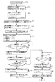
【図1】本実施例におけるバッテリ充放電装置の電気的構成図である。
【図2】(a)は、充電ドライブ回路の構成を概略的に表した図であり、(b)は、放電ドライブ回路の構成を概略的に表した図である。
【図3】(a)は、充電ドライブ回路の指令電圧生成回路への入力電圧波形を示した図であり、(b)は、指令電圧生成回路の出力電圧波形を示した図であり、(c)は、バッテリへの充電電流波形を示した図であり、(d)は、放電ドライブ回路の指令電圧生成回路への入力電圧波形を示した図であり、(e)は、指令電圧生成回路の出力電圧波形を示した図であり、(f)は、バッテリからの放電電流波形を示した図である。
【図4】バッテリ充放電装置のメイン処理を示したフローチャートである。
【図5】バッテリ再生前処理を示したフローチャートである。
【図6】バッテリ再生充放電処理を示したフローチャートである。
【図7】バッテリ放電処理を示したフローチャートである。
【図8】バッテリ充電処理を示したフローチャートである。
【図9】(a)は、充電電圧測定処理を示したフローチャートであり、(b)は、放電電圧測定処理を示したフローチャートである。
【符号の説明】
1 バッテリ充放電装置(バッテリ再生装置)
2 直流電源回路
3 制御ユニット(充電制御手段)
4 充電スイッチング回路
6 電流電圧変換回路
11 放電回路
12 放電スイッチング回路
24 タイマ回路(充電計時手段の一部)
48a 充電ドライブ回路の指令電圧生成回路(充電駆動回路)
48c 電流フィードバック回路(帰還増幅回路)
49a 放電ドライブ回路の指令電圧生成回路(放電駆動回路)
61 バッテリ(車載用鉛バッテリ)
61a 正極端子
73 充電指令電圧の一例(充電駆動基準電圧の一例)
73a パルス充電指令電圧の一例(充電駆動パルス電圧の一例)
73b ベース充電指令電圧の一例(充電駆動ベース電圧の一例)
74 充電電流の一例
74a パルス充電電流の一例(充電電流のパルス電流成分の一例)
74b ベース充電電流の一例(充電電流のベース電流成分の一例)
78 放電電流の一例
IGBT1 絶縁ゲート型バイポーラトランジスタ(電圧制御型スイッチング素子)
t2 パルス出力時間(充電電流のパルス電流成分が通電されている期間)
t4 ベース出力時間(充電電流のベース電流成分が通電されている期間)[0001]
TECHNICAL FIELD OF THE INVENTION
The present invention relates to a battery regenerating device for restoring the capacity of a lead battery for vehicle use and further charging the battery, and more particularly, to recover the capacity by removing the sulfate deposited on the electrode surface of the lead battery for vehicle use, and to improve the sulfation of the lead battery. The present invention relates to a battery regenerative charger capable of charging a vehicle lead battery in parallel with removal.
[0002]
[Prior art]
At present, lead storage batteries, which are a kind of secondary batteries (storage batteries), are inexpensive compared to other storage batteries, and are therefore widely used as power sources for electric equipment for vehicles. In general, the capacity of a vehicle-mounted lead storage battery (vehicle-mounted lead battery) is significantly reduced due to various causes when charging and discharging are repeated. For example, in-vehicle lead batteries used for a period of about two to three years may have a capacity reduced to about 50% as compared with unused ones, and it is impossible to supply power to loads such as electric equipment for vehicles. turn into. The in-vehicle lead battery whose capacity has been reduced in this way is judged to have reached the end of its life, and is discarded.
[0003]
By the way, various causes can be considered for the reduction of the capacity of the above-mentioned lead battery for vehicle use, one of which is due to sulfation. Sulfation is a hard film in which lead sulfate is largely crystallized, and has almost no electron conductivity or ionic conductivity. For example, when the charge / discharge of the vehicle-mounted lead battery is repeated for a predetermined period or the natural discharge with time is continued for a predetermined period, the electrolyte stored in the lower part of the vehicle-mounted lead battery becomes high. It is formed on the lower surface of the electrode plate by the phenomenon of specific gravity (stratification).
[0004]
Generally, an electrode plate of a lead battery for a vehicle is formed in a spongy body having a large number of pores on its surface, and as a result, its surface area is increased and its capacity is increased. However, the surface of the electrode plate of the lead battery for a vehicle on which sulfation has occurred is blocked by the crystallized lead sulfate, so that the surface area of the electrode plate decreases. As a result, the capacity of the on-vehicle lead battery is reduced, and the internal resistance is significantly increased.
[0005]
Therefore, in recent years, various treatment methods have been proposed to remove the sulfation from the electrode surface and recover the capacity of the vehicle-mounted lead battery. As one example, a direct current pulse current is applied to the vehicle-mounted lead battery to reduce the electrode surface. There is a treatment method for electrolyzing the accumulated sulfation. According to the on-vehicle lead battery capacity recovery process, a pulse current wave obtained by turning on and off a DC current of about 1 to 8 A (ampere) at a frequency of several kHz to several tens kHz is transmitted to the on-vehicle lead battery for a predetermined time. By applying a current, the sulfation is removed from the electrode surface.
[0006]
[Problems to be solved by the invention]
However, according to the above-described vehicle lead battery capacity recovery processing, sulfation is removed by applying a DC pulse current to the vehicle-mounted lead battery for a predetermined time, but only such a DC pulse current is applied to the lead storage battery. Then, there was a problem that the in-vehicle lead battery could not be charged to a fully charged state. That is, after the capacity of the vehicle-mounted lead battery is recovered by the above-described capacity recovery process, it is necessary to further perform a charging process on the vehicle-mounted lead battery. There was a problem that becomes.
[0007]
The present invention has been made in order to solve the above-described problems, and removes sulfation deposited on the electrode surface of a vehicle-mounted lead battery to reduce the capacity of the vehicle-mounted lead battery to a value corresponding to an almost unused state. It is another object of the present invention to provide a battery regenerating apparatus capable of recovering a battery and recovering the sulfation and charging a lead battery for a vehicle in parallel with the removal of the sulfate.
[0008]
[Means for Solving the Problems]
In order to achieve this object, a battery regeneration device according to claim 1 includes a DC power supply circuit for generating a DC current, and a charging current inserted between the DC power supply circuit and the vehicle-mounted lead battery to flow into the vehicle-mounted lead battery. A charge switching circuit for turning on or off the current supply, and charge control means for turning on or off the charge switching circuit.HaveThe charging control means outputs a charging driving pulse voltage that changes in a substantially rectangular waveform with respect to a substantially constant charging driving base voltage.Superimposed at a frequency of 2 kHzCharge drive circuit for outputting a charge drive reference voltage to the charge switching circuitCharge drive command means for commanding the output of a charge drive reference voltage to the charge drive circuit; charge time means for counting the execution time of the charge drive command means; Charge interval means for prohibiting execution of the charge drive command means for a predetermined time every time elapsesWherein the charging switching circuit includes a control terminal connected directly or indirectly to an output terminal of the charging drive circuit, an input terminal connected to an output terminal of the DC power supply circuit, and the vehicle lead. A voltage-controlled switching element having an output terminal connected to the positive terminal of the battery, the voltage-controlled switching element having a charge drive pulse voltage of the charge drive reference voltage output from the charge drive circuit. And a base current component proportional to the charge drive base voltage of the charge drive reference voltage.At a frequency of 2kHzThe charging current that changes periodically and alternately is supplied to the output terminal of the voltage-controlled switching element.
[0009]
According to the battery regeneration device of the first aspect, the charge control means outputs the charge drive reference voltage from the charge drive circuit. The charging drive reference voltage is obtained by superimposing a substantially rectangular charging drive pulse voltage on a substantially constant charging drive base voltage, and is output to the control terminal of the voltage-controlled switching element of the charging switching circuit. The voltage-controlled switching element is turned on when a charge drive reference voltage is directly or indirectly applied to its control terminal, and a charge current proportional to the charge drive reference voltage is supplied from the DC power supply circuit to the vehicle lead battery. Turn on electricity.
[0010]
Specifically, when the output of the charge drive reference voltage is instructed to the charge drive circuit by the execution of the charge drive instruction means, the charge drive circuit outputs the charge drive reference. When the execution time of the charge driving command means elapses over the charging limit time based on the time measured by the charging timing means, the charging interval means prohibits the execution of the charging driving command means for a predetermined time every time the charging time elapses. The output of the charging drive reference voltage from the drive circuit is stopped, and the voltage-controlled switching element of the switching circuit is turned off. That is, the supply of the charging current to the vehicle lead battery is prohibited by the charging interval means for a predetermined time every time the charging limit time elapses. The energization of the charging current and the prohibition of the energization are repeatedly performed.
[0011]
Also,The charge current flowing into the vehicle lead battery is a pulse current component proportional to the charge drive pulse voltage of the charge drive reference voltage output from the charge drive circuit, and a base current proportional to the charge drive base voltage of the charge drive reference voltage. The components alternate periodically. That is, the charging current is a current in which a pulse current component that changes in a substantially rectangular wave shape is superimposed on a substantially constant base current component, and the pulse current component removes the sulfation deposited on the electrode surface of the lead-acid battery for vehicle use. The charging of the on-vehicle battery is reliably advanced by the base current component.
[0012]
According to a second aspect of the present invention, in the battery regeneration apparatus according to the first aspect, the charging control means detects a charging current supplied to an output terminal of the voltage-controlled switching element in proportion to the charging current. A current-voltage conversion circuit for converting the voltage into a voltage; and a control terminal of the voltage-controlled switching element by amplifying a deviation between a detection voltage converted by the current-voltage conversion circuit and a charge drive reference voltage output from the charge drive circuit. And a negative feedback amplifier circuit for applying the signal to the negative feedback amplifier.
[0013]
According to the battery regeneration device of the second aspect, it operates in the same manner as the battery regeneration device of the first aspect, and further includes a detection voltage of the charging current converted by the current-voltage conversion circuit and an output from the charging driving circuit. The charging drive reference voltage is input to the feedback amplifier circuit. Here, the charge drive reference voltage is a target voltage proportional to the charge current that is desired to flow between the input and output terminals of the voltage-controlled switching element, and the deviation between the charge drive reference voltage, which is the target voltage, and the detection voltage is determined by feedback amplification. The voltage is amplified by the circuit and applied to the control terminal of the voltage-controlled switching element as a control voltage.
[0014]
The control voltage applied to the voltage-controlled switching element is successively changed by the feedback amplifier circuit so as to match the detection voltage of the charging current and the reference voltage for driving the charging (that is, to reduce the deviation between the two voltages).,resultIn other words, a charging current closer to a charging current (a target value of the charging current) proportional to the charging drive reference voltage is supplied to the output terminal of the voltage-controlled switching element.
[0015]
BEST MODE FOR CARRYING OUT THE INVENTION
Hereinafter, preferred embodiments of the present invention will be described with reference to the accompanying drawings. FIG. 1 is an electrical configuration diagram of a battery charge / discharge device 1 in the present embodiment. The battery charging / discharging device 1 mainly controls a charging current supplied to a lead storage battery (battery) 61 used as a vehicle-mounted storage battery, thereby removing sulfation deposited on an electrode surface of the battery and supplementing the same. This is a device for charging (hereinafter simply referred to as “charging”).
[0016]
The battery charge / discharge device 1 has a rated output voltage of 12 V and a maximum of 40 A (ampere) from a single-phase three-wire AC power supply (hereinafter referred to as “AC power supply”) 60 of 100 V (volt) or 200 V. A DC
[0017]
The charging switching circuit 4 is a circuit for turning on or off the supply of the charging current supplied from the DC
[0018]
The gate terminal of the transistor IGBT1 (the control terminal of the voltage-controlled switching element) has an anode terminal of the Zener diode ZD1, the cathode terminal of the Zener diode ZD1 has the cathode terminal of the Zener diode ZD2, and the anode terminal of the Zener diode ZD2. The terminals are connected to the emitter terminals of the transistor IGBT1, respectively. With this connection, when the transistor IGBT1 is turned on and off, an overvoltage such as a surge voltage generated between the gate and the emitter terminal can be suppressed, and the transistor IGBT1 can be protected from the overvoltage.
[0019]
Between the gate and emitter terminals of the transistor IGBT1, a resistor R1 of 10 kΩ for protection and preventing floating of the gate voltage is inserted in parallel with the Zener diodes ZD1 and ZD2, and the gate terminal and the emitter terminal of the transistor IGBT1 are respectively connected. Separately, it is connected to the charging
[0020]
The
[0021]
As shown in FIG. 1, the current-voltage conversion circuit 6 converts the charging current into a voltage by passing the charging current (collector current of the transistor IGBT1) output from the charging switching circuit 4 from the input terminal to the output terminal. This is a circuit for outputting to the
[0022]
According to the current-voltage conversion circuit 6, the charging current (collector current of the transistor IGBT1) output from the charging switching circuit 4 is converted by the shunt resistor R2 to a voltage value obtained by multiplying the current value by 1/10. It is output to the
[0023]
The backflow prevention circuit 7 is a circuit for preventing the charging current output from the charging switching circuit 4 and the discharging current from the
[0024]
The
[0025]
The input terminal of the charging relay switch SW1 is connected to the output terminal of the backflow prevention circuit 7 (that is, the cathode terminals of the diodes D1 and D2), while the output terminal of the charging relay switch SW1 is connected to the
[0026]
The
[0027]
The current /
[0028]
Specifically, the current passing through the
[0029]
The discharge circuit 11 is a load circuit for discharging the
[0030]
The
[0031]
The other connection states of the transistor IGBT2, the Zener diodes ZD3, ZD4, and the resistor R7 in the
[0032]
As shown in FIG. 1, the current-
[0033]
Next, the
[0034]
The bus line 27 is also connected to an input /
[0035]
The
[0036]
The A / D converter 25 converts an analog voltage value (voltage data) input from the current /
[0037]
The
[0038]
The processing mode memory 23a is a memory for storing the selected processing mode. Here, the processing mode is a type of processing performed on the
[0039]
As described above, any value of “0” to “3” is stored in the processing mode memory 23a according to the selected processing mode. The selection of these four processing modes is performed by pressing one of the
[0040]
Here, there are a plurality of types of
[0041]
The minimum
[0042]
The unit processing time counter 23c is a time (actual charging continuation time) during which a current is actually allowed to flow into the
[0043]
For example, in the present embodiment, when “0” is stored in the processing mode memory 23a and the pre-reproduction processing mode is selected, the unit processing time counter 23c has a value corresponding to the actual charging duration of 30 minutes as an initial value. Is set. When “1” or “2” is stored in the processing mode memory 23a and the small-capacity processing mode or the medium-capacity processing mode is selected, the actual charge continuation time of 5 minutes (or the actual discharge continuation time) The value corresponding to (time) is set as an initial value of the unit processing time counter 23c. Further, when "3" is stored in the processing mode memory 23a and the large-capacity processing mode is selected, a value corresponding to an actual charging duration (or an actual discharging duration) of 8 minutes is expressed in units. This is set as an initial value of the processing time counter 23c.
[0044]
The charging
[0045]
For example, in the battery charging process of FIG. 8, the actual charging duration is 5 minutes in the case of the small capacity processing mode or the medium capacity processing mode, and an interval of 3 minutes is provided after the lapse of the actual charging duration. The execution time of the battery charging process per one time is about 8 minutes. When eight hours (480 minutes) are divided by approximately eight minutes, which is the execution time of this one battery charging process, the result is 60. Therefore, in the case of the small-capacity processing mode and the medium-capacity processing mode, 60 is set as the initial value of the charging
[0046]
In addition, in the case of the large capacity processing mode, the actual charging duration is 8 minutes, and the interval time of 3 minutes is provided after the actual charging duration has elapsed. Is about 11 minutes.
[0047]
The
[0048]
The terminal voltage memory 23f is a memory for temporarily storing a terminal voltage value of the
[0049]
The
[0050]
The
[0051]
The base voltage memory 23i stores the voltage (base voltage) value applied to the
[0052]
The discharge completion flag 23j is a flag indicating whether or not it is necessary to execute the battery discharge process of FIG. 7 for the
[0053]
The forced termination flag 23k is a flag indicating whether it is necessary to forcibly terminate the battery regeneration charging / discharging process in FIG. 6 in the battery discharging process in FIG. This forced end flag 23k is set to an off state by initialization of the
[0054]
The charging
[0055]
The
[0056]
The
[0057]
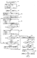
The
[0058]
As shown in FIG. 2A, the charging
[0059]
A charge drive command output from the D /
[0060]
The
[0061]
The
[0062]
As shown in FIG. 2B, the
[0063]
The discharge command voltage input to the input terminal of the insulating amplifier ISO2 of the insulating
[0064]
The operation of the
[0065]
First, in the battery charging process, the D /
[0066]
The
[0067]
Here, the
[0068]
The command
[0069]
The pulse
[0070]
The
[0071]
The charging current 74 is obtained by alternately repeating a 15A pulse charging current (pulse current component) 74a and an 8V base charging current (base current component) 74b. Specifically, the charging current 74 is held for a pulse output time t2 of 125 μs for the pulse charging current 74a and then for a base output time t4 of 375 μs for the base charging current 74b. As described above, according to the charging current 74 in which the pulse charging current 74a of a large current that changes in a substantially rectangular wave shape is superimposed on the substantially constant base charging current 74b, the large current flows into the
[0072]
The pulse charging current 74a is 8A in the small capacity processing mode, 25A in the large capacity processing mode, and 2A in the pre-playback processing mode. The base charging current 74b is 3A in the small capacity processing mode, 10A in the large capacity processing mode, and 15A in the pre-playback processing mode.
[0073]
FIG. 3D is a diagram illustrating an input voltage waveform to the command
[0074]
First, in the battery discharge process, the D /
[0075]
The
[0076]
The
[0077]
When the gate voltage and the gate current are applied to the gate terminal, the transistor IGBT2 is turned on, and the collector current (discharge current) of 8A is applied between the collector and the emitter terminal of the transistor IGBT2 from the
[0078]
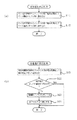
Next, the operation of the battery charge / discharge device 1 configured as described above will be described with reference to the flowcharts of FIGS. FIG. 4 is a flowchart showing main processing of the battery charge / discharge device 1. This main process is a process executed when the power switch of the battery charge / discharge device 1 is turned on. In this process, first, the value in the
[0079]
When any of the
[0080]
After the
[0081]
FIG. 5 is a flowchart illustrating the battery regeneration pre-processing. The battery regeneration pretreatment is mainly performed on the
[0082]
In the battery pre-processing, first, a counter value corresponding to 30 minutes is written into the unit processing time counter 23c (S21), and then the terminal voltage of the
[0083]
After the energization in S24, the counting of the value stored in the unit processing time counter 23c, that is, the counting of 30 minutes is started (S25), and the output of the 3V charging drive command is started while monitoring the time of the
[0084]
The charge control command of 2.8 V is continued for the base output time t4 of 375 μs (S30: No), the base output time t4 elapses (S30: Yes), and the unit processing time from the start of time measurement in S25. If the time corresponding to the value stored in the counter 23c has not elapsed (S31: No), the process proceeds to S27, and the processes from S27 to S30 are repeated. The charge drive command and the charge control command are converted into a charge command voltage via a command
[0085]
After passing through the
[0086]
The charging current is adjusted by a gate voltage applied to the gate terminal of the transistor IGBT1 of the charging switching circuit 4, and the gate voltage is determined according to a charging drive command and a charging control command output from the D /
[0087]
After the end of the counting of the value stored in the unit processing time counter 23c (S31: Yes), the charge drive command and the charge control command are set to 0V (S32), and the transistor IGBT1 of the charge switching circuit 4 is turned off. Then, by stopping the current supply to the charging operation coil 29 (S33), the charging system relay switch SW1 is turned off to stop the flow of the charging current into the
[0088]
When three minutes have elapsed after the processing of S33 (S34: Yes), the terminal voltage of the
[0089]
On the other hand, in the process of S23, when the value written to the terminal voltage memory 23f is less than 1 V (S23: No), the
[0090]
FIG. 6 is a flowchart showing the battery regeneration charging / discharging process. This battery regeneration charging / discharging process recovers the capacity of the
[0091]
In the battery regeneration charging / discharging process, first, a counter value corresponding to one hour is written to the minimum
[0092]
Thereafter, the terminal voltage of the
[0093]
In the process of S46, when the value of the terminal voltage memory 23f is equal to or higher than the discharge switching voltage value of 15V (S46: Yes), the
[0094]
In the battery discharge process shown in FIG. 7, first, the value of the terminal voltage memory 23f is written into the
[0095]
After setting the actual discharge duration time (S72), by energizing both the charging
[0096]
After the energization in S73, time counting for the value stored in the unit processing time counter 23c is started (S74), and output of a 3V discharge drive command is started while monitoring the time of the timer circuit 24 (S75). Together with the output of the discharge drive command, a discharge control command of 2.7 V when the value of the processing mode memory 23 a is “1”, 2.2 V when it is “2”, and 2.0 V when it is “3” Is started (S76), and the output of the discharge drive command and the discharge control command described above is continued until the counting of the value of the unit processing time counter 23c ends (S77: No).
[0097]
The discharge drive command and the discharge control command are given by the command
[0098]
After the end of the time counting for the value stored in the unit processing time counter 23c (S77: Yes), the discharge drive command and the discharge control command are set to 0 V (S78), and the transistor IGBT2 of the
[0099]
After the stop, if the forcible end flag 23k is turned on (S80: Yes), "Forced end because the discharge end voltage has been reached" is displayed on the LCD 40 (S81), and S10 of the main process of FIG. By shifting to (S82), the battery discharging process is completed, and the process stands by until the
[0100]
When three minutes have elapsed after the processing of S79 (S83: Yes), the terminal voltage of the
[0101]
Returning to FIG. In the process of S48, the difference between the value of the terminal voltage memory 23f and the value of the
[0102]
On the other hand, if the voltage value indicated by the difference between the value of the terminal voltage memory 23f and the value of the
[0103]
In the processing after S53, first, it is determined whether or not timekeeping for the value stored in the minimum
[0104]
In the battery charging process shown in FIG. 8, first, when the value of the processing mode memory 23a is "1" or "2", a value corresponding to 5 minutes is set, and when the value is "3", a value corresponding to 8 minutes is set. Is written to the unit processing time counter 23c (S91), the actual charging continuation time in one battery charging process is set, and the charging
[0105]
After the energization in S92, the counting of the value stored in the unit processing time counter 23c is started (S93), and the output of the 3V charging drive command is started while monitoring the time of the timer circuit 24 (S94). After the output of the charge drive command, a discharge control command of 2.2 V when the value of the processing mode memory 23 a is “1”, 1.5 V when “2”, and 0.5 V when “3”. Is started (S95), and the output of the charge drive command and the charge control command is continued for a pulse output time t2 of 125 μs (S96: No).
[0106]
When the pulse output time t2 elapses (S96: Yes), the output of the charge drive command of 3V is held, and the value of the processing mode memory 23a is 2.7V when the value of the processing mode memory 23a is "1" and 2.7 when the value of the processing mode memory 23a is "2". In the case of 2.2 V and "3", the output of the charge control command of 2.0 V is started (S97), and the output of the charge drive command and the charge control command is continued for the base output time t4 of 375 μs. (S98: No).
[0107]
If the base output time t4 has elapsed (S98: Yes), and the time corresponding to the value stored in the unit processing time counter 23c has not elapsed since the start of the time measurement in S93 (S99: No), 3V The process proceeds to S95 while holding the output of the charge drive command, and the processes from S95 to S98 are repeated. The operations of the
[0108]
The charging current is adjusted by a gate voltage applied to the gate terminal of the transistor IGBT1 of the charging switching circuit 4, and the gate voltage is determined according to a charging drive command and a charging control command output from the D /
[0109]
Specifically, in the small capacity processing mode, the pulse charging current of 8 A and the base charging current of 3 A are 5 minutes, and in the medium capacity processing mode, the pulse charging current of 15 A and the base charging current of 8 A are 5 minutes. In the large-capacity processing mode, the pulse charging current of 5 A and the base charging current of 10 A alternately flow into the
[0110]
After the end of the counting of the value stored in the unit processing time counter 23c (S99: Yes), the charge drive command and the charge control command are set to 0V (S100), and the transistor IGBT1 of the charge switching circuit 4 is turned off. By stopping the power supply to the charging operation coil 29 (S101), the charging system relay switch SW1 is turned off to stop the flow of the charging current into the
[0111]
When three minutes have elapsed after the processing of S101 (S102: Yes), the terminal voltage of the
[0112]
Returning to FIG. After the battery charging process (S55), when the value of the terminal voltage memory 23f is less than the charge completion voltage value of 13.5V (S56: No), or when the value of the terminal voltage memory 23f is 13.5V If the value is not less than the discharge switching voltage value of 15 V (S56: Yes, S57: No), it is determined whether or not the value of the
[0113]
On the other hand, if the value of the terminal voltage memory 23f is equal to or higher than the discharge switching voltage value of 15 V in the process of S57 (S57: Yes), it is determined whether the discharge completion flag 23j is on or off (S58), and the discharge completion flag 23j is turned off. In this case, the process proceeds to the battery discharging process in S47. On the other hand, when the discharge flag 23j is on, the values of the
[0114]
If the value of the base voltage memory 23i is less than the base voltage limit value of 14.5 V (S60), it is determined whether or not the time measurement for the value of the minimum
[0115]
FIG. 9A shows a flowchart of the charging voltage measurement process. This charging voltage measurement process is executed at intervals of 30 ms to measure the terminal voltage of the
[0116]
FIG. 9B shows a flowchart of the discharge voltage measurement process. This discharge voltage measurement process is an interrupt process executed every 30 ms to measure the terminal voltage of the
[0117]
As a result of the determination, if the value of the terminal voltage memory 23f is equal to or higher than the discharge end voltage value of 10.5 V (S122: Yes), the discharge voltage measurement process is terminated as it is, but is lower than the discharge end voltage of 10.5V. In this case (S122: No), after setting the forced end flag 23k to the ON state (S123), the process proceeds to S78 of the battery discharge process shown in FIG. 7 (S124), and this discharge voltage measurement process is ended. The processing from S78 to S82 of the battery discharging processing shown in FIG. 7 is executed. That is, the battery discharge process is forcibly terminated by the process of S124 in FIG. 9B. This is executed to suppress such overdischarge because the
[0118]
It should be noted that the charging drive instructing means of the third aspect is the processing of S94, S95 and S97 in FIG. 8, the charging timer means is the processing of S94, the charging interval means is the branch of Yes in S99, the processing of S100 and the processing of S102. No. branch corresponds to each.
[0119]
As described above, the present invention has been described based on the embodiments. However, the present invention is not limited to the above-described embodiments, and it is easily understood that various improvements and modifications can be made without departing from the spirit of the present invention. It can be inferred.
[0120]
For example, in this embodiment, an insulated gate bipolar transistor has been described as an example of the voltage control type switching element of the present invention. However, such a voltage control type switching element is not necessarily limited to this. Other switching elements may be used.
[0121]
In this embodiment, in order to generate the 15A pulse charging current 74a and the 8A base charging current 74b shown in FIG. 3C, the 3V charging
[0122]
However, the charge drive circuit for generating the pulse charge current of 15 A and the base charge current of 8 A shown in FIG. 3C is not necessarily limited to this. For example, a charge drive command of 0.8 V and a high output May be input to the command voltage generation circuit of the charge drive circuit. In such a case, if the command voltage generation circuit is configured to output a voltage obtained by adding the charge drive command and the charge control command, the command voltage generation circuit outputs a charge drive command of 0.8 V when the charge control command is high. A pulse charge command voltage of 1.5 V in which a charge control command of 0.7 V is superimposed on the command is output. When a low charge control command is output, a charge control command of 0 V is superimposed on a charge drive command of 0.8 V. It is possible to output a base charge command voltage of 8V.
[0123]
Further, in the present embodiment, the number of the
[0124]
Further, in the present embodiment, the description has been made using the charge drive command of 3 V. However, the value of the charge drive command is not necessarily limited to this, and may be set to 5 V corresponding to the drive voltage of the
[0125]
Hereinafter, modified examples of the present invention will be described. The battery regeneration device according to any one of claims 1 to 3, wherein a discharge circuit through which a discharge current flowing from the vehicle-mounted lead battery flows, and a flow of the discharge current flowing from the vehicle-lead battery into the discharge circuit is turned on or off. A discharge switching circuit, a discharge driving circuit for turning on or off the discharge switching circuit, and a pulse voltage component for measuring a terminal voltage of the lead battery for vehicle use during a period when the pulse current component of the charging current is supplied by the charging switching circuit. Measuring means, and first discharging means for turning on the discharge switching circuit by the discharge driving circuit when the terminal voltage of the vehicle lead battery is equal to or higher than the pulse voltage component limit value as a result of the measurement by the pulse voltage component measuring means. A battery regeneration device 1 comprising: 9A as the pulse voltage component measuring means of the battery regeneration device 1, the Yes branch of S59 of FIG. 6 and the processing of S75 and S76 of FIG. 7 as the first discharging means. Applicable respectively.
[0126]
In the battery regenerating device 1 or the battery regenerating device according to any one of claims 1 to 3, a discharge circuit through which a discharge current supplied from the vehicle lead battery flows, and the vehicle lead battery flows into the discharge circuit. A discharge switching circuit for turning on or off the supply of a discharge current, a discharge drive circuit for turning on or off the discharge switching circuit, and a lead-acid battery for a vehicle in a period in which a base current component of the charge current is supplied by the charge switching circuit Base voltage component measuring means for measuring the terminal voltage of the vehicle, and as a result of the measurement by the base voltage component measuring means, when the terminal voltage of the vehicle lead battery is equal to or higher than the base voltage component limit value, the discharge driving circuit performs the discharge switching. And a second discharging means for turning on the circuit.
[0127]
【The invention's effect】
According to the battery regeneration device of the present invention, the charging switching circuit causes the charging current flowing into the lead battery for vehicle to be a current in which a pulse current component that changes in a substantially rectangular wave shape is superimposed on a substantially constant base current component. Sulfation deposited on the electrode surface of the on-vehicle lead battery is removed by the pulse current component, and the capacity of the on-vehicle lead battery can be restored to a value substantially equivalent to an unused state.
[0128]
In addition, since the base current component flows into the vehicle lead battery when the pulse current component of the charging current is not supplied, the charging of the vehicle lead battery can be reliably advanced by the base current component. There is an effect that the charging progress speed of the lead battery for vehicle can be accelerated by the current component. As a result, since it is not necessary to perform a charging process on the lead-acid battery for the vehicle after the lead-acid battery for the vehicle has been subjected to the capacity recovery processing as in the related art, the operation can be simplified to process a large amount of the lead-acid battery for the vehicle. In addition, the processing cost can be reduced.
[0129]
Further, the supply of the charging current to the on-vehicle lead-acid battery is prohibited for a predetermined time by the charging interval means every time the charging limit time elapses, so that the execution of the charge driving command means is prohibited by the charging interval means. In addition, there is an effect that the in-vehicle lead battery that has been overheated by the inflow of the charging current is radiated, and an excessive rise in temperature of the in-vehicle lead battery can be suppressed.
[0130]
According to the battery regeneration device of the second aspect, the control voltage applied to the control terminal of the voltage-controlled switching element is adjusted by the feedback amplifier circuit so that the detection voltage of the charging current matches the charging driving reference voltage, that is, However, since the deviation between the two voltages is adjusted so as to decrease, even when the internal resistance of the vehicle lead battery or the output power of the DC power supply circuit fluctuates according to the charging status, it is proportional to the charging drive reference voltage. There is an effect that the charged current thus obtained can be reliably supplied to the output terminal of the voltage-controlled switching element.
[Brief description of the drawings]
FIG. 1 is an electrical configuration diagram of a battery charge / discharge device according to an embodiment.
FIG. 2A is a diagram schematically illustrating a configuration of a charge drive circuit, and FIG. 2B is a diagram schematically illustrating a configuration of a discharge drive circuit.
FIG. 3A is a diagram illustrating an input voltage waveform to a command voltage generation circuit of a charging drive circuit, and FIG. 3B is a diagram illustrating an output voltage waveform of the command voltage generation circuit; (c) is a diagram showing a charging current waveform to the battery, (d) is a diagram showing an input voltage waveform to a command voltage generation circuit of the discharge drive circuit, and (e) is a diagram showing the command voltage generation. FIG. 7 is a diagram illustrating an output voltage waveform of the circuit, and FIG. 7F is a diagram illustrating a discharge current waveform from the battery.
FIG. 4 is a flowchart showing main processing of the battery charge / discharge device.
FIG. 5 is a flowchart showing a battery regeneration pre-process.
FIG. 6 is a flowchart showing a battery regeneration charging / discharging process.
FIG. 7 is a flowchart showing a battery discharging process.
FIG. 8 is a flowchart showing a battery charging process.
9A is a flowchart illustrating a charging voltage measurement process, and FIG. 9B is a flowchart illustrating a discharge voltage measurement process.
[Explanation of symbols]
1 Battery charging / discharging device (battery regeneration device)
2 DC power supply circuit
3 control unit (charge control means)
4 Charge switching circuit
6. Current-voltage conversion circuit
11 Discharge circuit
12 Discharge switching circuit
24 Timer circuit (part of charging timekeeping means)
48a Command voltage generation circuit of charge drive circuit (charge drive circuit)
48c Current feedback circuit (feedback amplifier circuit)
49a Discharge drive circuit command voltage generation circuit (discharge drive circuit)
61 Battery (lead battery for vehicle)
61a Positive terminal
73 Example of charge command voltage (example of charge drive reference voltage)
73a Example of pulse charge command voltage (example of charge drive pulse voltage)
73b Example of base charge command voltage (example of charge drive base voltage)
74 Example of charging current
74a Example of pulse charging current (example of pulse current component of charging current)
74b Example of base charging current (example of base current component of charging current)
78 Example of discharge current
IGBT1 Insulated gate bipolar transistor (voltage controlled switching element)
t2 pulse output time (period during which the pulse current component of the charging current is supplied)
t4 Base output time (period during which the base current component of the charging current is supplied)
Claims (2)
その直流電源回路及び車載用鉛バッテリ間に挿入されその車載用鉛バッテリへ流入させる充電電流の通電をオン又はオフする充電スイッチング回路と、
その充電スイッチング回路をオン又はオフさせる充電制御手段とを備えており、
前記充電制御手段は、
略一定の充電駆動ベース電圧に対して略矩形波状に変化する充電駆動パルス電圧を2kHzの周波数で重畳させた充電駆動基準電圧を前記充電スイッチング回路へ出力する充電駆動回路と、
その充電駆動回路に対して充電駆動基準電圧の出力を指令する充電駆動指令手段と、
その充電駆動指令手段の実行時間を計時する充電計時手段と、
その充電計時手段による計時が充電制限時間を経過する毎に前記充電駆動指令手段の実行を所定時間禁止する充電インターバル手段とを備えており、
前記充電スイッチング回路は、
その充電駆動回路の出力端に直接又は間接的に接続される制御端と、前記直流電源回路の出力端に接続される入力端と、前記車載用鉛バッテリの正極端子に接続される出力端とを有した電圧制御型スイッチング素子を備えており、
その電圧制御型スイッチング素子は、
前記充電駆動回路から出力される前記充電駆動基準電圧の充電駆動パルス電圧に比例したパルス電流成分、及び、前記充電駆動基準電圧の充電駆動ベース電圧に比例したベース電流成分が2kHzの周波数で周期的に交互に変化する充電電流を、その電圧制御型スイッチング素子の出力端へ通電させるものであることを特徴とするバッテリ再生装置。A DC power supply circuit for generating a DC current,
A charge switching circuit that is inserted between the DC power supply circuit and the lead battery for vehicle and that turns on or off the flow of charging current flowing into the lead battery for vehicle,
Charge control means for turning on or off the charge switching circuit ,
The charging control means,
A charge drive circuit that outputs to the charge switching circuit a charge drive reference voltage in which a charge drive pulse voltage that changes in a substantially rectangular waveform with respect to a substantially constant charge drive base voltage is superimposed at a frequency of 2 kHz ;
Charge drive command means for commanding the output of a charge drive reference voltage to the charge drive circuit;
Charge timing means for timing the execution time of the charge drive command means;
Charge interval means for prohibiting the execution of the charge drive command means for a predetermined time each time the time counted by the charge time means elapses the charge limit time ,
The charging switching circuit,
A control terminal connected directly or indirectly to an output terminal of the charge driving circuit, an input terminal connected to an output terminal of the DC power supply circuit, and an output terminal connected to a positive terminal of the lead battery for vehicle use; A voltage-controlled switching element having
The voltage-controlled switching element is
A pulse current component proportional to the charge drive pulse voltage of the charge drive reference voltage output from the charge drive circuit and a base current component proportional to the charge drive base voltage of the charge drive reference voltage are periodically generated at a frequency of 2 kHz. A battery regenerating apparatus characterized in that a charging current that changes alternately is supplied to an output terminal of the voltage-controlled switching element.
その電流電圧変換回路により変換された検出電圧と前記充電駆動回路から出力される充電駆動基準電圧との偏差を増幅して前記電圧制御型スイッチング素子の制御端へ印加する負帰還増幅回路とを備えていることを特徴とする請求項1記載のバッテリ再生装置。A current-voltage conversion circuit that converts a charging current supplied to an output terminal of the voltage-controlled switching element into a detection voltage proportional to the charging current;
A negative feedback amplifier circuit for amplifying a deviation between a detection voltage converted by the current-voltage conversion circuit and a charge drive reference voltage output from the charge drive circuit, and applying the amplified voltage to a control terminal of the voltage-controlled switching element. The battery regeneration device according to claim 1, wherein:
Priority Applications (1)
| Application Number | Priority Date | Filing Date | Title |
|---|---|---|---|
| JP2002033977A JP3564458B2 (en) | 2002-02-12 | 2002-02-12 | Battery regeneration device |
Applications Claiming Priority (1)
| Application Number | Priority Date | Filing Date | Title |
|---|---|---|---|
| JP2002033977A JP3564458B2 (en) | 2002-02-12 | 2002-02-12 | Battery regeneration device |
Publications (2)
| Publication Number | Publication Date |
|---|---|
| JP2003235174A JP2003235174A (en) | 2003-08-22 |
| JP3564458B2 true JP3564458B2 (en) | 2004-09-08 |
Family
ID=27776618
Family Applications (1)
| Application Number | Title | Priority Date | Filing Date |
|---|---|---|---|
| JP2002033977A Expired - Fee Related JP3564458B2 (en) | 2002-02-12 | 2002-02-12 | Battery regeneration device |
Country Status (1)
| Country | Link |
|---|---|
| JP (1) | JP3564458B2 (en) |
Families Citing this family (11)
| Publication number | Priority date | Publication date | Assignee | Title |
|---|---|---|---|---|
| JP4749095B2 (en) * | 2005-09-12 | 2011-08-17 | 武次 西田 | Storage battery regeneration processing method |
| JP5373317B2 (en) * | 2008-05-19 | 2013-12-18 | 有限会社オーエイチケー研究所 | Battery regenerator and battery regenerating method |
| KR100931510B1 (en) * | 2009-01-12 | 2009-12-11 | (주)마루엠씨에스 | Battery regeneration device |
| JP5533010B2 (en) * | 2010-02-22 | 2014-06-25 | 株式会社デンソー | Battery voltage monitoring device |
| KR101124768B1 (en) | 2010-07-21 | 2012-03-23 | 김순자 | A Life Extending and Recycling Equipment for Automobile Rechargeable Battery |
| KR101582186B1 (en) * | 2010-11-02 | 2016-01-21 | 김정욱 | Recycling Device For Rechargeable Battery |
| CN103840211A (en) * | 2012-11-20 | 2014-06-04 | 江苏富朗特新能源有限公司 | Movable lithium ion battery forming apparatus |
| KR101963930B1 (en) * | 2015-02-09 | 2019-03-29 | 고려대학교 산학협력단 | Energy storage system with lead acid battery and method for charging and discharging lead acid battery |
| JP6885688B2 (en) | 2016-08-01 | 2021-06-16 | トヨタ自動車株式会社 | How to regenerate nickel metal hydride batteries |
| JPWO2020065773A1 (en) * | 2018-09-26 | 2021-09-02 | アレクJapan株式会社 | Lead battery regeneration device and lead battery regeneration method |
| JP7108962B2 (en) | 2018-12-03 | 2022-07-29 | 株式会社オートネットワーク技術研究所 | In-vehicle backup power supply control device and in-vehicle backup power supply device |
-
2002
- 2002-02-12 JP JP2002033977A patent/JP3564458B2/en not_active Expired - Fee Related
Also Published As
| Publication number | Publication date |
|---|---|
| JP2003235174A (en) | 2003-08-22 |
Similar Documents
| Publication | Publication Date | Title |
|---|---|---|
| JP2743155B2 (en) | Charger and charge processing system | |
| JP3564458B2 (en) | Battery regeneration device | |
| US20110057624A1 (en) | battery charging device and method | |
| JPH097641A (en) | Charging method of secondary battery | |
| JP2004364387A (en) | Charging method of secondary battery, charger, and charge control program thereof | |
| JPS6159048B2 (en) | ||
| CN102457077A (en) | Apparatus and method for recycling and charging simultaneously a battery | |
| KR101004762B1 (en) | Battery Restoration Device and Method | |
| CN110198059B (en) | Method for charging an energy store | |
| JP2003189498A (en) | Charging method and charger of secondary battery | |
| JP2002191136A (en) | Battery charger | |
| JP2005027435A (en) | Charger | |
| JP2002017050A (en) | Rechargeable battery charging circuit | |
| JP2001145271A (en) | Protection method and protection circuit for secondary battery | |
| JPH07271681A (en) | Backup circuit for semiconductor memory | |
| JP2010129538A (en) | Method for reproducing lead storage battery and reproducing apparatus thereof | |
| JPH10201111A (en) | Charge control method and charge control device | |
| CN222127690U (en) | A charging start circuit of a charger | |
| CN215185976U (en) | Power supply circuit and electronic equipment | |
| JP3450676B2 (en) | Secondary battery device | |
| JP2543889B2 (en) | Charge control device | |
| JP2656060B2 (en) | Storage battery charge control circuit | |
| JP3403916B2 (en) | Method and device for charging secondary battery | |
| JP3003210B2 (en) | How to charge lead storage batteries | |
| JPH02168820A (en) | Charge/discharge switching device for battery |
Legal Events
| Date | Code | Title | Description |
|---|---|---|---|
| A977 | Report on retrieval |
Free format text: JAPANESE INTERMEDIATE CODE: A971007 Effective date: 20040105 |
|
| A131 | Notification of reasons for refusal |
Free format text: JAPANESE INTERMEDIATE CODE: A131 Effective date: 20040113 |
|
| A521 | Written amendment |
Free format text: JAPANESE INTERMEDIATE CODE: A523 Effective date: 20040315 |
|
| TRDD | Decision of grant or rejection written | ||
| A01 | Written decision to grant a patent or to grant a registration (utility model) |
Free format text: JAPANESE INTERMEDIATE CODE: A01 Effective date: 20040511 |
|
| A61 | First payment of annual fees (during grant procedure) |
Free format text: JAPANESE INTERMEDIATE CODE: A61 Effective date: 20040607 |
|
| R150 | Certificate of patent or registration of utility model |
Ref document number: 3564458 Country of ref document: JP Free format text: JAPANESE INTERMEDIATE CODE: R150 Free format text: JAPANESE INTERMEDIATE CODE: R150 |
|
| S303 | Written request for registration of pledge or change of pledge |
Free format text: JAPANESE INTERMEDIATE CODE: R316303 |
|
| R360 | Written notification for declining of transfer of rights |
Free format text: JAPANESE INTERMEDIATE CODE: R360 |
|
| R370 | Written measure of declining of transfer procedure |
Free format text: JAPANESE INTERMEDIATE CODE: R370 |
|
| S303 | Written request for registration of pledge or change of pledge |
Free format text: JAPANESE INTERMEDIATE CODE: R316303 |
|
| R350 | Written notification of registration of transfer |
Free format text: JAPANESE INTERMEDIATE CODE: R350 |
|
| R250 | Receipt of annual fees |
Free format text: JAPANESE INTERMEDIATE CODE: R250 |
|
| FPAY | Renewal fee payment (event date is renewal date of database) |
Free format text: PAYMENT UNTIL: 20080611 Year of fee payment: 4 |
|
| FPAY | Renewal fee payment (event date is renewal date of database) |
Free format text: PAYMENT UNTIL: 20090611 Year of fee payment: 5 |
|
| R250 | Receipt of annual fees |
Free format text: JAPANESE INTERMEDIATE CODE: R250 |
|
| FPAY | Renewal fee payment (event date is renewal date of database) |
Free format text: PAYMENT UNTIL: 20100611 Year of fee payment: 6 |
|
| R250 | Receipt of annual fees |
Free format text: JAPANESE INTERMEDIATE CODE: R250 |
|
| FPAY | Renewal fee payment (event date is renewal date of database) |
Free format text: PAYMENT UNTIL: 20100611 Year of fee payment: 6 |
|
| FPAY | Renewal fee payment (event date is renewal date of database) |
Free format text: PAYMENT UNTIL: 20110611 Year of fee payment: 7 |
|
| R250 | Receipt of annual fees |
Free format text: JAPANESE INTERMEDIATE CODE: R250 |
|
| FPAY | Renewal fee payment (event date is renewal date of database) |
Free format text: PAYMENT UNTIL: 20110611 Year of fee payment: 7 |
|
| FPAY | Renewal fee payment (event date is renewal date of database) |
Free format text: PAYMENT UNTIL: 20120611 Year of fee payment: 8 |
|
| R250 | Receipt of annual fees |
Free format text: JAPANESE INTERMEDIATE CODE: R250 |
|
| FPAY | Renewal fee payment (event date is renewal date of database) |
Free format text: PAYMENT UNTIL: 20130611 Year of fee payment: 9 |
|
| R250 | Receipt of annual fees |
Free format text: JAPANESE INTERMEDIATE CODE: R250 |
|
| FPAY | Renewal fee payment (event date is renewal date of database) |
Free format text: PAYMENT UNTIL: 20130611 Year of fee payment: 9 |
|
| S111 | Request for change of ownership or part of ownership |
Free format text: JAPANESE INTERMEDIATE CODE: R313113 |
|
| S531 | Written request for registration of change of domicile |
Free format text: JAPANESE INTERMEDIATE CODE: R313531 |
|
| FPAY | Renewal fee payment (event date is renewal date of database) |
Free format text: PAYMENT UNTIL: 20130611 Year of fee payment: 9 |
|
| R350 | Written notification of registration of transfer |
Free format text: JAPANESE INTERMEDIATE CODE: R350 |
|
| FPAY | Renewal fee payment (event date is renewal date of database) |
Free format text: PAYMENT UNTIL: 20130611 Year of fee payment: 9 |
|
| S803 | Written request for registration of cancellation of provisional registration |
Free format text: JAPANESE INTERMEDIATE CODE: R316803 |
|
| FPAY | Renewal fee payment (event date is renewal date of database) |
Free format text: PAYMENT UNTIL: 20130611 Year of fee payment: 9 |
|
| R360 | Written notification for declining of transfer of rights |
Free format text: JAPANESE INTERMEDIATE CODE: R360 |
|
| FPAY | Renewal fee payment (event date is renewal date of database) |
Free format text: PAYMENT UNTIL: 20130611 Year of fee payment: 9 |
|
| R360 | Written notification for declining of transfer of rights |
Free format text: JAPANESE INTERMEDIATE CODE: R360 |
|
| R360 | Written notification for declining of transfer of rights |
Free format text: JAPANESE INTERMEDIATE CODE: R360 |
|
| R250 | Receipt of annual fees |
Free format text: JAPANESE INTERMEDIATE CODE: R250 |
|
| R370 | Written measure of declining of transfer procedure |
Free format text: JAPANESE INTERMEDIATE CODE: R370 |
|
| S321 | Written request for registration of change in pledge agreement |
Free format text: JAPANESE INTERMEDIATE CODE: R316321 |
|
| S803 | Written request for registration of cancellation of provisional registration |
Free format text: JAPANESE INTERMEDIATE CODE: R316803 |
|
| R350 | Written notification of registration of transfer |
Free format text: JAPANESE INTERMEDIATE CODE: R350 |
|
| R250 | Receipt of annual fees |
Free format text: JAPANESE INTERMEDIATE CODE: R250 |
|
| R250 | Receipt of annual fees |
Free format text: JAPANESE INTERMEDIATE CODE: R250 |
|
| R250 | Receipt of annual fees |
Free format text: JAPANESE INTERMEDIATE CODE: R250 |
|
| R250 | Receipt of annual fees |
Free format text: JAPANESE INTERMEDIATE CODE: R250 |
|
| R250 | Receipt of annual fees |
Free format text: JAPANESE INTERMEDIATE CODE: R250 |
|
| R250 | Receipt of annual fees |
Free format text: JAPANESE INTERMEDIATE CODE: R250 |
|
| R250 | Receipt of annual fees |
Free format text: JAPANESE INTERMEDIATE CODE: R250 |
|
| LAPS | Cancellation because of no payment of annual fees |