JP3568739B2 - Wafer polishing equipment - Google Patents
Wafer polishing equipment Download PDFInfo
- Publication number
- JP3568739B2 JP3568739B2 JP15557797A JP15557797A JP3568739B2 JP 3568739 B2 JP3568739 B2 JP 3568739B2 JP 15557797 A JP15557797 A JP 15557797A JP 15557797 A JP15557797 A JP 15557797A JP 3568739 B2 JP3568739 B2 JP 3568739B2
- Authority
- JP
- Japan
- Prior art keywords
- wafer
- retainer ring
- carrier
- head
- polishing
- Prior art date
- Legal status (The legal status is an assumption and is not a legal conclusion. Google has not performed a legal analysis and makes no representation as to the accuracy of the status listed.)
- Expired - Lifetime
Links
- 238000005498 polishing Methods 0.000 title claims description 73
- 230000002093 peripheral effect Effects 0.000 claims description 16
- 238000001514 detection method Methods 0.000 claims description 5
- 235000012431 wafers Nutrition 0.000 description 122
- 230000007246 mechanism Effects 0.000 description 27
- 230000008859 change Effects 0.000 description 5
- 238000005336 cracking Methods 0.000 description 5
- 238000006073 displacement reaction Methods 0.000 description 5
- 238000007517 polishing process Methods 0.000 description 5
- 239000012530 fluid Substances 0.000 description 4
- 239000012634 fragment Substances 0.000 description 4
- 230000000694 effects Effects 0.000 description 3
- 230000000149 penetrating effect Effects 0.000 description 3
- 239000004065 semiconductor Substances 0.000 description 3
- 238000000034 method Methods 0.000 description 2
- 238000000926 separation method Methods 0.000 description 2
- XUIMIQQOPSSXEZ-UHFFFAOYSA-N Silicon Chemical compound [Si] XUIMIQQOPSSXEZ-UHFFFAOYSA-N 0.000 description 1
- 239000006061 abrasive grain Substances 0.000 description 1
- 230000008901 benefit Effects 0.000 description 1
- 239000000919 ceramic Substances 0.000 description 1
- 230000003111 delayed effect Effects 0.000 description 1
- 230000005489 elastic deformation Effects 0.000 description 1
- 239000013013 elastic material Substances 0.000 description 1
- 229920001971 elastomer Polymers 0.000 description 1
- 239000007788 liquid Substances 0.000 description 1
- 239000000463 material Substances 0.000 description 1
- 230000009467 reduction Effects 0.000 description 1
- 230000004044 response Effects 0.000 description 1
- 239000005060 rubber Substances 0.000 description 1
- 229910052710 silicon Inorganic materials 0.000 description 1
- 239000010703 silicon Substances 0.000 description 1
- 239000002002 slurry Substances 0.000 description 1
- XLYOFNOQVPJJNP-UHFFFAOYSA-N water Substances O XLYOFNOQVPJJNP-UHFFFAOYSA-N 0.000 description 1
Images



Landscapes
- Finish Polishing, Edge Sharpening, And Grinding By Specific Grinding Devices (AREA)
- Mechanical Treatment Of Semiconductor (AREA)
Description
【0001】
【発明の属する技術分野】
本発明は、集積回路を形成する半導体ウェーハ等の表面を研磨するためのウェーハ研磨装置に係わり、特に、ウェーハ保持ヘッドがフローティングヘッド構造とされたウェーハ研磨装置に関する。
【0002】
【従来の技術】
この種のウェーハ研磨装置としては、表面に研磨パッドが貼付された円盤状のプラテンと、研磨すべきウェーハの一面を保持して研磨パッドにウェーハの他面を当接させる複数のウェーハ保持ヘッドとを具備し、これらウェーハ保持ヘッドと前記プラテンとを相対運動させつつ研磨パッドとウェーハの間に研磨砥粒を含むスラリーを供給することにより研磨を行うものが広く知られている。
【0003】
その一例として、研磨パッドに対するウェーハの当接圧力を均一化することができるといった利点を有するフローティングヘッド構造を採用したウェーハ保持ヘッドが開示されている(米国特許5,205,082号)。
【0004】
このウェーハ保持ヘッドは、図8に示すように、中空のヘッド本体1と、ヘッド本体1内に水平に張られたダイアフラム2と、ダイアフラム2の下面に固定されたキャリア3とを備え、ダイアフラム2によって画成された空気室4に、シャフト5を通じて加圧空気源6から加圧空気を供給することにより、キャリア3を下方へ押圧する構成とされている。
【0005】
また、キャリア3の外周には、下端がキャリア3よりも下方に突出するようにリテーナリング7が配置され、キャリア3の下面に付着したウェーハの外周を保持するとともに研磨中のウェーハがキャリア3から外れるといった不具合を防止するようなっている。
【0006】
【発明が解決しようとする課題】
しかしながら、近年のウェーハ大径化に伴う研磨面積の増大により、ウェーハ研磨時におけるウェーハと研磨パッドとの間の摩擦抵抗が増大しており、このため、ウェーハをキャリア3の下面に設けた吸水性のウェーハ付着シートによって表面張力で保持するようにした水貼り法では、研磨中のウェーハがリテーナリング7と研磨パッドとの間に入り込むようにウェーハ保持ヘッドから外れ、滑り出たウェーハが他のウェーハ保持ヘッドに衝突して割れや欠けが生じたり、その破片により研磨パッド,キャリア3およびリテーナリング7が損傷することがあるといった不都合が生じている。
【0007】
また、キャリア3の下面に吸着孔を形成し、該吸着孔に接続される吸引手段等によりウェーハを真空吸着して保持性を高める真空吸着法もあるが、この場合には、吸着孔付近で局所的な圧力差が生じて研磨量が不均一になり、平滑な仕上げ面を得ることができないという問題が生じ得る。
【0008】
本発明は、上記事情に鑑みてなされたもので、ウェーハがキャリアから滑り出したことを検知可能とすることにより、ウェーハやウェーハ研磨装置の損傷を未然に防止し得るウェーハ研磨装置を提供することを目的とする。
【0009】
【課題を解決するための手段】
本発明は、前記課題を解決するために以下の構成を採用した。
請求項1記載のウェーハ研磨装置は、表面に研磨パッドが貼付されたプラテンと、研磨すべきウェーハの一面を保持して前記研磨パッドにウェーハの他面を当接させる1または2以上のウェーハ保持ヘッドとを具備し、これらウェーハ保持ヘッドと前記プラテンとの相対運動により前記研磨パッドでウェーハ他面を研磨するウェーハ研磨装置であって、
前記ウェーハ保持ヘッドは、研磨すべきウェーハの前記一面を保持するための円盤状のキャリアと、該キャリアの外周に同心状に配置されかつヘッド軸線方向に変位可能なリテーナリングと、円筒状に形成され前記リテーナリングを同心状かつ内部に配し内周面で該リテーナリングを支持するヘッド本体とを備えるとともに、該ヘッド本体に、研磨中のウェーハが前記キャリアから滑り出したことを検知する検知手段が設けられ、前記検知手段は、前記リテーナリングに作用する半径外方向の圧力を検出する圧力センサと、該圧力センサからの出力信号によりウェーハが前記キャリアから滑り出したか否かを判断する滑り判断手段とを備えた構成であることを特徴とするものである。
【0010】
このウェーハ研磨装置 では、研磨中のウェーハがキャリアから滑り出すと、ウェーハがリテーナリングと研磨パッドとの間に入り込んでウェーハがリテーナリングの内面を押圧しなくなるので、リテーナリングに作用する半径外方向の圧力の減少を圧力センサによって検出することができる。
【0011】
したがって、圧力センサからの出力信号を受けた滑り判断手段は、検出された圧力の減少量と、あらかじめ設定した基準値とを比較する等してウェーハが滑り出したか否かの状態を判断することができる。
【0012】
また、このウェーハ研磨装置では、検知手段により研磨中のウェーハがキャリアから滑り出したことを検知することができるので、例えば、検知手段からの出力信号により警報を発することができる警報装置を設け、該装置から警報が発せられた場合に手動でウェーハ研磨装置 を停止するようにしたり、ウェーハ研摩装置を前記出力信号に応じて制御することができるように構成して自動的に緊急停止させる等の対策を講じることができる。
【0017】
【発明の実施の形態】
以下、本発明に係るウェーハ研磨装置の第一の実施形態を図1から図4を参照しながら説明する。
【0018】
始めに、図3および図4を参照して全体の構成を簡単に説明する。
これらの図中、符号11は基台であり、この基台11の中央には円盤状のプラテン12が水平に設置されている。
このプラテン12は基台11内に設けられたプラテン駆動機構(図示略)により軸線回りに回転されるようになっており、その上面には全面に亙って研磨パッド13が貼付されている。
【0019】
プラテン12の上方には、複数の支柱14を介して上側取付板15が水平に設置されている。
この上側取付板15の下面には円盤状のカルーセル16が設置されている。
このカルーセル16は、上側取付板15上に設けられたカルーセル駆動機構(図示略)により軸線回りに回転されるようになっており、その下面にはプラテン12と対向する計6基のウェーハ保持ヘッド17が設けられている。
【0020】
これらウェーハ保持ヘッド17は、図4に示すように、カルーセル16の中心から同一距離においてカルーセル16の中心軸回りに60゜毎に配置されており、それぞれ、ヘッド駆動機構(図示略)により周方向に回転させられるとともに、カルーセル駆動機構により遊星回転させられるようになっている。
なお、ウェーハ保持ヘッド17の個数は6基に限定されず、1〜5基または7基以上でもよい。
【0021】
次に、図1を参照して、本実施形態に係るウェーハ保持ヘッド17について説明する。
ウェーハ保持ヘッド17は、軸線が垂直に配置されるとともに下端が開口する中空のヘッド本体18と、このヘッド本体18の内部に張られた第1のダイアフラム19Aおよび第2のダイアフラム19Bと、この第1のダイアフラム19Aの下面に固定された円盤状のキャリア20と、該キャリア20の外周に同心に配置されたリテーナリング21とを具備するものである。
【0022】
前記ヘッド本体18は、円板状の天板部18aと、この天板部18aの外周に固定される円筒状の周壁部18bとから構成され、天板部18aはカルーセル16のシャフト22に同軸に固定されている。
この周壁部18bの内周面には、全周に亙って半径内方向に突出する円環状段部の取付部23が形成されている。
【0023】
前記キャリア20は、セラミック等の高い剛性を有する材料で成形された一定厚さのものであり、弾性変形はしない。
前記リテーナリング21は、下端面が平坦な円環状をなし、キャリア20の外周面との間に僅かなクリアランスをもって同心状に配置され、キャリア20とは独立して上下変位可能とされている。
【0024】
また、リテーナリング21の上端外周縁には、半径外方向に突出する保持部21Aが形成されており、ウェーハ保持ヘッド17をカルーセル16と共にプラテン22から引き上げた場合に、この保持部21Aが周壁部18bの下端の円環状のストッパ部24により保持されるようになっている。
【0025】
該ストッパ部24は、周壁部18bの下端周縁から半径内方向に突出し、リテーナリング21の外周に当接状態若しくは僅かなクリアランスをもってリテーナリング21を取り囲んで形成されている。
【0026】
前記キャリア20の上面には、第1のダイアフラム19Aの内縁部が軸線を同じくして配されるとともに、リテーナリング21の上面には、第1のダイアフラム19Aの外縁部が配されている。
【0027】
第1のダイアフラム19Aの内縁部の上面には、軸線を同じくして第1の固定リング25が配され、該第1の固定リング25は、第1の固定リング25および第1のダイアフラム19Aを貫通する複数のボルト26によって第1のダイアフラム19Aを挟持した状態でキャリア20に固定されている。
【0028】
また、第1のダイアフラム19Aの外縁部の上面には、軸線を同じくして連結用リング27が配され、該連結用リング27の上面には第2のダイアフラム19Bの内縁部が配されている。
【0029】
そして、第2のダイアフラム19Bの内縁部上面には、軸線を同じくして第2の固定リング28が配され、該第2の固定リング28は、第1のダイアフラム19A、連結用リング27、第2のダイアフラム19Bおよび第2の固定リング28を貫通する複数のボルト29によって第1のダイアフラム19Aおよび第2のダイアフラム19Bをそれぞれ挟持した状態でリテーナリング21に固定されている。
【0030】
さらに、第2のダイアフラム19Bの外縁部は取付部23に載せられ、前記外縁部上面には、軸線を同じくして第3の固定リング30が配されている。
該第3の固定リング30は、第2のダイアフラム19Bおよび第3の固定リング30を貫通する複数のボルト31によって、第2のダイアフラム19Bを挟持した状態で取付部23に固定されている。
【0031】
そして、第1のダイアフラム19Aと第2のダイアフラム19Bは、各種ゴム等の弾性材料で形成され、これによりリテーナリング21はヘッド本体18の周壁部18bとは独立に上下変位可能になっている。
【0032】
前記ヘッド本体18の天板部18aには、当該天板部18aをヘッド本体18の軸線と平行に貫通するとともに先端が所定の間隔をおいて前記固定リング28に対向するように配される位置センサ32が3箇所以上設けられている。
【0033】
位置センサ32には、例えば、静電容量式のセンサが用いられ、この場合には、当該位置センサ32の先端に設けられた電極と、前記固定リング28の頭部基準面28aに設けられた電極との間における電気容量の変化を、これら電極間の離間距離の変化、すなわちリテーナリング21の変位として検出することができる。
【0034】
ウェーハ保持ヘッド17の外部に設けられた研磨機制御系33には、位置センサ32からの出力信号を受けるとともにその出力信号から研磨パッド13に対するリテーナリング21の上下方向の相対変位と、あらかじめ設定した基準値とを比較してウェーハWが滑り出したか否かの判断を行う滑り判断手段が設けられ、該滑り判断手段からの出力信号に応じて、前記ヘッド駆動機構,カルーセル駆動機構及びプラテン駆動機構を緊急停止できるように構成されている。
【0035】
一方、シャフト22には流路が形成され、ヘッド本体18、キャリア20、第1のダイアフラム19Aおよび第2のダイアフラム19Bにより画成された流体室34は、流路を通じて圧力調整機構である加圧手段35に接続されている。
【0036】
そして、加圧手段35で流体室34内の流体圧力を調整することにより、第1のダイアフラム19Aおよび第2のダイアフラム19Bが上下に変位して研磨パッド13へのキャリア20の押圧力が変化するようになっている。
なお、流体としては、一般に空気を使用すれば十分であるが、必要に応じて他種のガスや液体を使用してもよい。
【0037】
上記構成からなるウェーハ研磨装置では、研磨工程中、ウェーハWは研磨パッド13との摩擦力によってリテーナリング21の内周に押圧されており、ウェーハWに過度の摩擦力が作用した場合、図2に示すように、研磨中のウェーハWがリテーナリング21と研磨パッド13との間に入り込むように滑り始める場合がある。
【0038】
この場合、位置センサ32の先端に設けられた電極と、リテーナリング21に一体に固定された固定リング28の頭部基準面28Aに設けられた電極との間の電気容量の変化が、これら電極間の離間距離の変化、すなわち研磨パッド13に対するリテーナリング21の上方向への相対変位として検出される。
【0039】
そして、滑り判断手段は、位置センサ32により検出された上方向の相対変位が、あらかじめ設定した基準値を越えるものであると、ウェーハWがキャリア20から滑り出した状態であるものと判断し、その出力信号を受けた研磨機制御系33によって、前記ヘッド駆動機構,カルーセル駆動機構及びプラテン駆動機構は緊急停止させられる。
【0040】
このように、本実施形態に係るウェーハ研磨装置によれば、研磨中のウェーハWがキャリア20から滑り出すと、研磨パッド13に対するリテーナリング21の相対変位が位置センサ32により検出されるとともに、滑り判断手段により位置センサ32の出力信号からウェーハWが滑り出したか否かが判断されて、前記ヘッド駆動機構,カルーセル駆動機構及びプラテン駆動機構を緊急停止させることができるので、ウェーハWがウェーハ保持ヘッド17から外れ、この滑り出したウェーハWが他のウェーハ保持ヘッド17に衝突して割れや欠けが生じたり、その破片により研磨パッド13,キャリア20およびリテーナリング21が損傷するといったことを未然に防ぐことができる。
【0041】
次に、図5および図6を参照して、本発明の第二の実施形態に係るウェーハ保持ヘッド41について説明する。
各図において、前記第一の実施形態に係るウェーハ保持ヘッド17と同一構成の部分については、同一の符号を付すとともに、その説明を省略する。
【0042】
本実施形態のウェーハ保持ヘッド41は、図5に示すように、ヘッド本体42の平板部42aに前記位置センサ32は設けられておらず、代わりに周壁部42bの下端に設けられた円環状のストッパ部43に圧力センサ44が設けられている点で前記第一の実施形態に係るウェーハ保持ヘッド17と異なる構成になっている。
【0043】
圧力センサ44は、その先端の受感面を前記ストッパ部43の内周面に僅かに突出するように半径内方向に向けて設けられており、前記受感面にはピエゾ抵抗効果を測定するシリコンチップ等の半導体素子が配されて、外部に設けられた研磨機制御系45に無線により、または、スリップリング(図示略)を介して接続されている。
【0044】
研磨機制御系45は、前記半導体素子で検出された圧力信号から圧力の減少量とあらかじめ設定した基準値とを比較してウェーハWがキャリア20から滑り出したか否かを判断する滑り判断手段とを備え、該滑り判断手段からの出力信号に応じて前記ヘッド駆動機構,カルーセル駆動機構及びプラテン駆動機構を緊急停止できるように構成されている。
【0045】
上記構成のウェーハ研磨装置では、研磨工程中、キャリア20に保持されたウェーハWは研磨パッド13から受ける摩擦力によってリテーナリング21の内周面に押圧されており、その押圧力は、リテーナリング21を介してその外周面に受感面が当接させられた圧力センサ44によって半径外方向に加わる圧力として検出される。
【0046】
そして、ウェーハWに過度の摩擦力が作用すると、図6に示すように、研磨中のウェーハWがリテーナリング21と研磨パッド13との間に入り込むように滑り出す場合がある。
この場合、ウェーハWはリテーナリング21の内周面を押圧しなくなるので、リテーナリング21に作用する半径外方向の圧力の減少を圧力センサ44によって検出することができる。
【0047】
そして、滑り判断手段は、圧力センサ44により検出された圧力の減少量が、あらかじめ設定した基準値よりも大きいと、ウェーハWがキャリア20から滑り出した状態であると判断し、その出力信号を受けた研磨機制御系45によって、前記ヘッド駆動機構,カルーセル駆動機構及びプラテン駆動機構は緊急停止させられる。
【0048】
このように、本実施形態に係るウェーハ研磨装置によれば、研磨中のウェーハWがキャリア20から滑り出すと、リテーナリング21に作用する半径外方向の圧力の減少が圧力センサ44によって検出されるとともに、滑り判断手段により圧力センサ44の出力信号からウェーハWが滑り出したか否かが判断されて、ヘッド駆動機構,カルーセル駆動機構及びプラテン駆動機構を緊急停止させることができるので、ウェーハWがウェーハ保持ヘッド17から外れ、この滑り出したウェーハWが他のウェーハ保持ヘッド17に衝突して割れや欠けが生じたり、その破片により研磨パッド13,キャリア20およびリテーナリング21が損傷するといったことを未然に防ぐことができる。
【0049】
なお、本実施形態では、圧力センサ44を1箇所にのみ設けた構成を図示したが、複数箇所に設けることによって、より正確かつ迅速なウェーハWの滑り出しの検出を可能にすることができる。
すなわち、研磨加工中、リテーナリング21はウェーハ保持ヘッド41内で偏芯運動をしているためストッパ部43に対して接触・離間を周期的に繰り返しており、圧力センサ44が1箇所にのみ設けられた構成であると、検知が遅れたり誤検知する場合がある。
【0050】
したがって、かかる場合にも正確かつ迅速にウェーハWの滑り出しを検出することができるように、圧力センサ44は、図7(a)および同図(b)に示すように、3箇所以上設けておくことが望ましい。
【0051】
また、本実施形態に係るウェーハ研磨装置では、ウェーハ研磨の終点も検知することが可能である。
すなわち、ウェーハWの被研磨面は、研磨が進むに従い平滑になるため、該被研磨面と研磨パッド13との接触面積が増加してウェーハWに作用する摩擦抵抗が次第に大きくなり、これに伴いキャリア20からリテーナリング21に作用する半径外方向の圧力も次第に大きくなるため、ウェーハWの研磨量に応じて変化する圧力から研磨の終点を検出することができる。
【0052】
さらに、上記各実施形態では、研磨パッドに対するウェーハWの当接圧力を均一化することを目的として、第1のダイアフラム19Aおよび第2のダイアフラム19Bをそれぞれ別体としたものを図示したが、これらダイアフラム19A,19Bは、図8に示すような円形状に一体成形されたものであっても構わない。
【0053】
また、上記各実施形態では、ウェーハ保持ヘッド17を遊星回転させるカルーセル16が設けられたものについて説明したが、該カルーセル16が設けられておらず、前記ヘッド駆動機構によりウェーハ保持ヘッド17を周方向に回転させつつ前記プラテン駆動機構によりプラテン12を回転させてウェーハWの研摩を行うように構成されたものであっても構わない。
この場合には、前記滑り判断手段からの出力信号に応じてヘッド駆動機構及びプラテン駆動機構が緊急停止させられる。
【0054】
【発明の効果】
以上の説明から明らかなように、本発明に係るウェーハ研磨装置によれば、次のような効果を奏することができる。
(1)請求項1記載のウェーハ研磨装置 によれば、研磨中のウェーハがキャリアから滑り出すと、リテーナリングに作用する半径外方向の圧力の減少が圧力センサによって検出されるとともに、滑り判断手段によりウェーハが滑り出したか否かが判断されるので、滑り出したウェーハが他のウェーハ保持ヘッドに衝突して割れや欠けが生じたり、その破片により研磨パッド,キャリアおよびリテーナリングが損傷するといったことを未然に防ぐことができる。
【0055】
また、検知手段からの出力信号により警報を発することができる警報装置を設け、該装置から警報が発せられた場合に手動でウェーハ研磨装置 を停止するようにしたり、ウェーハ研摩装置を前記出力信号に応じて制御することができるように構成して自動的に緊急停止させるようにする等の対策を講じることができ、ウェーハの割れや欠け、研磨パッド,キャリアおよびリテーナリングの損傷を未然に防ぐことができる。
【図面の簡単な説明】
【図1】本発明に係るウェーハ研磨装置の第一の実施形態におけるウェーハ保持ヘッドを示す断面図である。
【図2】同装置によるウェーハの研磨工程中、ウェーハがキャリアから滑り出した状態を示す断面図である。
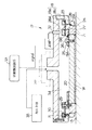
【図3】同装置の全体の構成を示す正面図である。
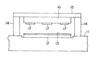
【図4】同装置のウェーハ保持ヘッドとプラテンの配置状態を示す平面図である。
【図5】本発明に係るウェーハ研磨装置の第二の実施形態におけるウェーハ保持ヘッドを示す断面図である。
【図6】同装置によるウェーハの研磨工程中、ウェーハがキャリアから滑り出した状態を示す断面図である。
【図7】(a)は本発明に係るウェーハ研磨装置の他の実施形態におけるウェーハ保持ヘッドを示す平面図、
(b)は(a)のA−A線断面図である。
【図8】従来のウェーハ研磨装置におけるウェーハ保持ヘッドの一例を示す断面図である。
【符号の説明】
12 プラテン
13 研磨パッド
16 カルーセル
17、41 ウェーハ保持ヘッド
18、42 ヘッド本体
20 キャリア
21 リテーナリング
32 位置センサ
44 圧力センサ
W ウェーハ[0001]
TECHNICAL FIELD OF THE INVENTION
The present invention relates to a wafer polishing apparatus for polishing a surface of a semiconductor wafer or the like forming an integrated circuit, and more particularly to a wafer polishing apparatus in which a wafer holding head has a floating head structure.
[0002]
[Prior art]
As a wafer polishing apparatus of this type, a disk-shaped platen having a polishing pad attached to a surface thereof, a plurality of wafer holding heads for holding one surface of a wafer to be polished and abutting the other surface of the wafer on the polishing pad, It is widely known that the polishing is performed by supplying a slurry containing abrasive grains between a polishing pad and a wafer while relatively moving the wafer holding head and the platen.
[0003]
As one example, there is disclosed a wafer holding head employing a floating head structure having an advantage that a contact pressure of a wafer with a polishing pad can be made uniform (US Pat. No. 5,205,082).
[0004]
As shown in FIG. 8, the wafer holding head includes a hollow head main body 1, a
[0005]
A retainer ring 7 is arranged on the outer periphery of the
[0006]
[Problems to be solved by the invention]
However, the frictional resistance between the wafer and the polishing pad at the time of polishing the wafer has increased due to the increase in the polishing area accompanying the recent increase in the diameter of the wafer. In the water bonding method in which the wafer is held at the surface tension by the wafer adhering sheet, the wafer being polished is detached from the wafer holding head so as to enter between the retainer ring 7 and the polishing pad, and the wafer that has slid out is replaced with another wafer. Inconveniences such as cracking or chipping due to collision with the holding head and damage to the polishing pad, the
[0007]
There is also a vacuum suction method in which a suction hole is formed on the lower surface of the
[0008]
The present invention has been made in view of the above circumstances, and it is an object of the present invention to provide a wafer polishing apparatus capable of preventing damage to a wafer or a wafer polishing apparatus by enabling detection of a wafer sliding out of a carrier. Aim.
[0009]
[Means for Solving the Problems]
The present invention has the following features to attain the object mentioned above.
2. The wafer polishing apparatus according to claim 1, wherein a platen having a polishing pad affixed to a surface thereof, one or more wafers holding one surface of the wafer to be polished and bringing the other surface of the wafer into contact with the polishing pad. A wafer polishing apparatus comprising a head, and polishing the other surface of the wafer with the polishing pad by the relative movement of the wafer holding head and the platen,
The wafer holding head has a disc-shaped carrier for holding the one surface of the wafer to be polished, a retainer ring concentrically disposed on the outer periphery of the carrier and displaceable in the head axis direction, and formed in a cylindrical shape. A head body for concentrically and internally arranging the retainer ring and supporting the retainer ring on an inner peripheral surface thereof, and detecting means for detecting that the wafer being polished has slipped from the carrier in the head body. A pressure sensor for detecting a radial pressure acting on the retainer ring, and a slip determination means for determining whether a wafer has slipped from the carrier based on an output signal from the pressure sensor. And a configuration provided with:
[0010]
This wafer polishing machine Then, when the wafer being polished slides out of the carrier, the wafer enters between the retainer ring and the polishing pad and the wafer no longer presses the inner surface of the retainer ring, so the reduction in the radial pressure acting on the retainer ring is reduced. It can be detected by a pressure sensor.
[0011]
Therefore, the slip judging means which has received the output signal from the pressure sensor can judge the state of whether or not the wafer has slipped, for example, by comparing the detected decrease in pressure with a preset reference value. it can.
[0012]
Further, in this wafer polishing apparatus, since it is possible to detect that the wafer being polished has slipped out of the carrier by the detecting means, for example, an alarm device capable of issuing an alarm by an output signal from the detecting means is provided, Wafer polishing equipment manually when an alarm is issued from the equipment , Or the wafer polishing apparatus can be controlled in accordance with the output signal to automatically take an emergency stop.
[0017]
BEST MODE FOR CARRYING OUT THE INVENTION
Hereinafter, a first embodiment of a wafer polishing apparatus according to the present invention will be described with reference to FIGS.
[0018]
First, the overall configuration will be briefly described with reference to FIGS.
In these figures, reference numeral 11 denotes a base, and a disk-
The
[0019]
Above the
A disk-shaped carousel 16 is provided on the lower surface of the
The carousel 16 is rotated around an axis by a carousel driving mechanism (not shown) provided on the
[0020]
As shown in FIG. 4, these wafer holding
The number of wafer holding
[0021]
Next, the
The
[0022]
The
On the inner peripheral surface of the
[0023]
The
The
[0024]
A holding
[0025]
The
[0026]
The inner edge of the
[0027]
On the upper surface of the inner edge portion of the
[0028]
On the upper surface of the outer edge of the
[0029]
On the upper surface of the inner edge of the second diaphragm 19B, a
[0030]
Further, an outer edge of the second diaphragm 19B is placed on the mounting portion 23, and a
The
[0031]
The
[0032]
The top plate portion 18a of the head
[0033]
As the
[0034]
A polishing
[0035]
On the other hand, a flow path is formed in the
[0036]
Then, by adjusting the fluid pressure in the
As the fluid, it is generally sufficient to use air, but other types of gas or liquid may be used as needed.
[0037]
In the wafer polishing apparatus having the above configuration, during the polishing process, the wafer W is pressed against the inner periphery of the
[0038]
In this case, the change in electric capacitance between the electrode provided at the tip of the
[0039]
If the upward relative displacement detected by the
[0040]
As described above, according to the wafer polishing apparatus according to the present embodiment, when the wafer W being polished slides out of the
[0041]
Next, a
In each drawing, the same components as those of the
[0042]
As shown in FIG. 5, the
[0043]
The
[0044]
The polishing
[0045]
In the wafer polishing apparatus having the above configuration, during the polishing process, the wafer W held by the
[0046]
When an excessive frictional force acts on the wafer W, the wafer W being polished may slide out so as to enter between the
In this case, since the wafer W does not press the inner peripheral surface of the
[0047]
When the amount of decrease in the pressure detected by the
[0048]
As described above, according to the wafer polishing apparatus according to the present embodiment, when the wafer W being polished slides out of the
[0049]
In the present embodiment, the configuration in which the
That is, during the polishing process, the
[0050]
Therefore, in such a case, the
[0051]
Further, the wafer polishing apparatus according to the present embodiment can also detect the end point of wafer polishing.
That is, the surface to be polished of the wafer W becomes smoother as the polishing progresses, so that the contact area between the surface to be polished and the
[0052]
Furthermore, in each of the above-described embodiments, the
[0053]
In each of the above embodiments, the carousel 16 for planetary rotation of the
In this case, the head drive mechanism and the platen drive mechanism are stopped in an emergency according to the output signal from the slip determination means.
[0054]
【The invention's effect】
As is clear from the above description, according to the wafer polishing apparatus of the present invention, the following effects can be obtained.
(1) The wafer polishing apparatus according to claim 1. According to this, when the wafer being polished slides out of the carrier, a decrease in the radially outward pressure acting on the retainer ring is detected by the pressure sensor, and the slip determination means determines whether the wafer has slipped. In addition, it is possible to prevent the wafer that has slid out from colliding with another wafer holding head to cause cracking or chipping, or damage to the polishing pad, the carrier, and the retainer ring due to fragments thereof.
[0055]
Further, an alarm device which can issue an alarm by an output signal from the detection means is provided, and when an alarm is issued from the device, a wafer polishing apparatus is manually provided. Or to take measures such as automatically configuring the wafer polishing apparatus so that it can be controlled in accordance with the output signal to automatically stop the wafer, such as cracking or chipping of the wafer. In addition, damage to the polishing pad, the carrier and the retainer ring can be prevented.
[Brief description of the drawings]
FIG. 1 is a sectional view showing a wafer holding head in a first embodiment of a wafer polishing apparatus according to the present invention.
FIG. 2 is a cross-sectional view showing a state in which the wafer slides out of a carrier during a wafer polishing process by the same apparatus.
FIG. 3 is a front view showing the entire configuration of the same device.
FIG. 4 is a plan view showing an arrangement state of a wafer holding head and a platen of the apparatus.
FIG. 5 is a sectional view showing a wafer holding head in a second embodiment of the wafer polishing apparatus according to the present invention.
FIG. 6 is a cross-sectional view showing a state in which the wafer has slid out of the carrier during the wafer polishing process by the same apparatus.
FIG. 7A is a plan view showing a wafer holding head in another embodiment of the wafer polishing apparatus according to the present invention,
(B) is a sectional view taken along line AA of (a).
FIG. 8 is a sectional view showing an example of a wafer holding head in a conventional wafer polishing apparatus.
[Explanation of symbols]
12
Claims (1)
前記ウェーハ保持ヘッドは、研磨すべきウェーハの前記一面を保持するための円盤状のキャリアと、The wafer holding head, a disk-shaped carrier for holding the one surface of the wafer to be polished,
該キャリアの外周に同心状に配置されかつヘッド軸線方向に変位可能なリテーナリングと、A retainer ring disposed concentrically on the outer periphery of the carrier and displaceable in the head axis direction;
円筒状に形成され前記リテーナリングを同心状かつ内部に配し内周面で該リテーナリングを支持するヘッド本体とを備えるとともに、A head body that is formed in a cylindrical shape and that concentrically and internally arranges the retainer ring and supports the retainer ring on an inner peripheral surface;
該ヘッド本体に、研磨中のウェーハが前記キャリアから滑り出したことを検知する検知手段が設けられ、The head body is provided with a detection unit for detecting that the wafer being polished has slipped from the carrier,
前記検知手段は、前記リテーナリングに作用する半径外方向の圧力を検出する圧力センサと、A pressure sensor for detecting a radially outward pressure acting on the retainer ring;
該圧力センサからの出力信号によりウェーハが前記キャリアから滑り出したか否かを判断する滑り判断手段とを備えた構成であることを特徴とするウェーハ研磨装置。And a slip determining means for determining whether or not the wafer has slipped from the carrier based on an output signal from the pressure sensor.
Priority Applications (1)
| Application Number | Priority Date | Filing Date | Title |
|---|---|---|---|
| JP15557797A JP3568739B2 (en) | 1997-06-12 | 1997-06-12 | Wafer polishing equipment |
Applications Claiming Priority (1)
| Application Number | Priority Date | Filing Date | Title |
|---|---|---|---|
| JP15557797A JP3568739B2 (en) | 1997-06-12 | 1997-06-12 | Wafer polishing equipment |
Publications (2)
| Publication Number | Publication Date |
|---|---|
| JPH11860A JPH11860A (en) | 1999-01-06 |
| JP3568739B2 true JP3568739B2 (en) | 2004-09-22 |
Family
ID=15609098
Family Applications (1)
| Application Number | Title | Priority Date | Filing Date |
|---|---|---|---|
| JP15557797A Expired - Lifetime JP3568739B2 (en) | 1997-06-12 | 1997-06-12 | Wafer polishing equipment |
Country Status (1)
| Country | Link |
|---|---|
| JP (1) | JP3568739B2 (en) |
Families Citing this family (8)
| Publication number | Priority date | Publication date | Assignee | Title |
|---|---|---|---|---|
| US6663466B2 (en) * | 1999-11-17 | 2003-12-16 | Applied Materials, Inc. | Carrier head with a substrate detector |
| WO2005016595A1 (en) * | 2003-08-19 | 2005-02-24 | Nikon Corporation | Grinding apparatus, semiconductor device producing method using the same, and semiconductor device produced by the method |
| JP4814677B2 (en) | 2006-03-31 | 2011-11-16 | 株式会社荏原製作所 | Substrate holding device and polishing device |
| JP5210083B2 (en) * | 2008-08-05 | 2013-06-12 | 株式会社荏原製作所 | Polishing method and apparatus |
| JP6906425B2 (en) * | 2017-10-31 | 2021-07-21 | 株式会社荏原製作所 | Board processing equipment |
| CN117381660A (en) * | 2023-11-27 | 2024-01-12 | 西安奕斯伟材料科技股份有限公司 | Wafer adsorption method and device, wafer grinding equipment |
| US20250235977A1 (en) * | 2024-01-19 | 2025-07-24 | Applied Materials, Inc. | Polishing head with retaining ring wear sensing |
| CN119077607B (en) * | 2024-09-26 | 2025-12-26 | 华海清科(上海)半导体有限公司 | Carrier heads and chemical mechanical polishing equipment for wafer processing |
-
1997
- 1997-06-12 JP JP15557797A patent/JP3568739B2/en not_active Expired - Lifetime
Also Published As
| Publication number | Publication date |
|---|---|
| JPH11860A (en) | 1999-01-06 |
Similar Documents
| Publication | Publication Date | Title |
|---|---|---|
| US6872122B2 (en) | Apparatus and method of detecting a substrate in a carrier head | |
| US6343973B1 (en) | Carrier head with a substrate detection mechanism for a chemical mechanical polishing system | |
| US6547641B2 (en) | Carrier head with a substrate sensor | |
| JP4641345B2 (en) | Carrier head with substrate detector | |
| US6059636A (en) | Wafer polishing apparatus | |
| US6277009B1 (en) | Carrier head including a flexible membrane and a compliant backing member for a chemical mechanical polishing apparatus | |
| JP3568739B2 (en) | Wafer polishing equipment | |
| CN111922888B (en) | Edge polishing device and polishing method | |
| US20070111637A1 (en) | Substrate holding apparatus and polishing apparatus | |
| EP0616362A2 (en) | Method for polishing work piece and apparatus therefor | |
| KR100335569B1 (en) | Polishing head of chemical and mechanical apparatus for polishing wafer | |
| JP3438874B2 (en) | Jig for calibration of wafer polishing apparatus and calibration apparatus | |
| JP3185680B2 (en) | Wafer polishing apparatus and wafer polishing method | |
| EP1582294B1 (en) | Wafer polishing method. | |
| JP3731411B2 (en) | Wafer polishing equipment | |
| JP3183204B2 (en) | Wafer polishing equipment | |
| JPH08257893A (en) | Wafer polishing apparatus and polishing method | |
| CN120533607B (en) | A wafer polishing head and polishing equipment | |
| JPH09141550A (en) | Polishing method for thin substrate and polishing apparatus therefor | |
| JP2001121409A (en) | Wafer polishing head and polishing apparatus using the same | |
| JP2009095910A (en) | Wafer pop-out detecting mechanism for polishing device, and method of detecting pop-out of wafer | |
| JP3784477B2 (en) | Wafer polishing apparatus and wafer holding head used therefor | |
| KR20150018971A (en) | Chemical mechanical polishing apparatus with improved accuracy of monitoring controlled pressure | |
| KR20020088598A (en) | Method of conditioning polishing pad and Chemical mechanical polishing apparatus for performing the same | |
| KR20200078828A (en) | Substrate processing apparatus |
Legal Events
| Date | Code | Title | Description |
|---|---|---|---|
| A711 | Notification of change in applicant |
Free format text: JAPANESE INTERMEDIATE CODE: A711 Effective date: 20040326 |
|
| TRDD | Decision of grant or rejection written | ||
| A01 | Written decision to grant a patent or to grant a registration (utility model) |
Free format text: JAPANESE INTERMEDIATE CODE: A01 Effective date: 20040601 |
|
| A61 | First payment of annual fees (during grant procedure) |
Free format text: JAPANESE INTERMEDIATE CODE: A61 Effective date: 20040616 |
|
| R150 | Certificate of patent or registration of utility model |
Free format text: JAPANESE INTERMEDIATE CODE: R150 |
|
| FPAY | Renewal fee payment (event date is renewal date of database) |
Free format text: PAYMENT UNTIL: 20090625 Year of fee payment: 5 |
|
| FPAY | Renewal fee payment (event date is renewal date of database) |
Free format text: PAYMENT UNTIL: 20100625 Year of fee payment: 6 |