JP3572425B2 - Sample for measuring transmittance, method for preparing the sample, and method for measuring transmittance - Google Patents
Sample for measuring transmittance, method for preparing the sample, and method for measuring transmittance Download PDFInfo
- Publication number
- JP3572425B2 JP3572425B2 JP07017395A JP7017395A JP3572425B2 JP 3572425 B2 JP3572425 B2 JP 3572425B2 JP 07017395 A JP07017395 A JP 07017395A JP 7017395 A JP7017395 A JP 7017395A JP 3572425 B2 JP3572425 B2 JP 3572425B2
- Authority
- JP
- Japan
- Prior art keywords
- transmittance
- sample
- measurement
- loss
- less
- Prior art date
- Legal status (The legal status is an assumption and is not a legal conclusion. Google has not performed a legal analysis and makes no representation as to the accuracy of the status listed.)
- Expired - Lifetime
Links
Images




Landscapes
- Sampling And Sample Adjustment (AREA)
- Investigating Or Analysing Materials By Optical Means (AREA)
Description
【0001】
【産業上の利用分野】
本発明は光学素材、例えば多成分光学ガラス、合成石英ガラス、結晶材料等の透過率、例えば内部透過率(反射損失を含まない分光透過率)の高精度な測定に用いるサンプル及びその作製方法、測定方法に関するものである。特に、g線(436nm)、i線(365nm)リソグラフィーに代表される可視・紫外線光学系に使用される多成分光学ガラスや、KrF(248nm)、ArF(193nm)エキシマレ−ザリソグラフィーなどの300nm以下の紫外線光学系に使用される合成石英ガラス、結晶材料の透過率測定サンプルに関するものである。
【0002】
【従来の技術】
従来、シリコン等のウエハ上に集積回路の微細パターンを露光・転写する光リソグラフィー技術においては、ステッパと呼ばれる露光装置が用いられる。
このステッパの光源は、近年のLSIの高集積化に伴ってg線からi線へと短波長化が進められている。このようなステッパの照明系あるいは投影レンズに用いられる光学ガラスの内部透過率は、99.8%/cmあるいは99.9%/cm以上(内部吸収0.2%/cm、あるいは、0.1%/cm以下)が要求される。そして、さらなるLSIの高集積化に伴い、ステッパの光源はKrFやArFエキシマレーザーへと移行している。このようなエキシマレーザーステッパの照明系あるいは投影レンズには、もはや一般光学ガラスは使用できず、石英ガラスや蛍石などの素材に限定される。このようなエキシマレーザーステッパの照明系あるいは投影レンズに用いられる石英ガラス、蛍石においても、その内部透過率は99.8%/cmあるいは99.9%/cm以上が要求される。したがって、紫外光領域での上記光学素材の高透過率化を目指した開発が進められている。一方で、短波長化が進むにつれて、光学素材の内部透過率を高精度で測定することが技術的に非常に難しくなっている。したがって、光学素材の高透過率を達成するためには、まず第一に、このような微弱な吸収しか存在しない光学ガラスや合成石英ガラスや結晶材料等の内部透過率(内部吸収0.1%/cm程度)を精度良く測定し、評価可能な技術が不可欠である。
【0003】
【発明が解決しようとする課題】
内部透過率の測定方法としては日本光学硝子工業会規格JOGIS−17−82に光学ガラスの内部透過率の測定方法が規定されている。その他の光学素材である石英ガラスあるいは結晶材料についても、内部透過率の測定方法はこれに準ずるものである。この規定の中で、透過率測定サンプルの作製については、厚さ3mmと10mmの1対とし、両者共平行に対面を研磨すること、内部透過率の表示については、10mm厚のガラスに対する値で表示すること、また、小数点以下第3位を四捨五入しているため、測定精度は内部吸収1%/cmに過ぎず、特に内部透過率の測定誤差の問題が顕著になるi線、エキシマレーザー等の短波長域は対象とされていなかった。
【0004】
光学素材の透過率の測定方法において、内部吸収0.1%/cmを有意差として測定するためには、主に、以下に示す事項が検討される。
▲1▼基本性能の高い分光光度計を用いて分光透過率(反射損失込みの透過率)を測定する。
▲2▼市販の分光光度計において、測定光路内にサンプルを挿入することで生じる光路ずれに起因する透過率ずれを補正する。
▲3▼高精度な、すなわち測定誤差の少ないサンプルを作製する。
【0005】
▲1▼、▲2▼に関しては、装置の開発により、193nm、248nmにおける測定ゆらぎを3σで±0.01%を達成した。
また、平行光線である事で、屈折による光路のズレにより生じる、検出器として使用される光電子増倍管の光電面の感度むらの影響が、実質上無い装置を作製した。
【0006】
しかしながら、▲3▼に関しては、従来、透過率測定サンプルの規格が存在せず、サンプルの精度を規定する項目及び程度が定量化されていなかった。したがって、透過率測定サンプルの規格を実現する作製方法も示されていなかった。
【0007】
【課題を解決するための手段】
本発明者らは、光学素材の透過率の測定方法において、透過率測定サンプルの規格及び作製方法に起因する測定誤差を鋭意研究した。
そして、サンプルに起因する測定誤差要素を検討した結果、サンプルの研磨面の平行度、面精度、表面粗さが問題となることが解った。
【0008】
一般にサンプルの作製は評価する光学素材の一部を分光光度計のサンプル室に入るような形状に切り出し、厚さ方向の向かい合う二面を市販の研磨剤で光学研磨することにより行われる。
ここで、平行度とは、光学研磨面の向かい合う二面のうちの一面を基準とし、その基準面に対する傾き(角度)である。また、面精度とは研磨面の平面原器からのずれ量であり、表面粗さとは各光学研磨面の凹凸の高さである。
【0009】
本発明者らは、先に、平行度30秒以下、面精度を平行度と同程度以下、表面粗さrms=10Å以下のサンプルを用いることにより、光学素材の内部透過率を±0.1%以下の誤差で高精度に測定することが可能となることを提案した。
さらに、透過率測定サンプルを作製する際に使用した切削、研磨剤等の残留不純物や加工により発生した残留応力に起因する構造欠陥が光学素材の分光透過率の低下原因であることを見い出し、光学素材のサンプルの作製において、サンプルを表面粗さrms=10Å程度に前研磨した後、SiO2研磨剤でrms=10Å以下にする、あるは酸またはアルカリ処理することを特徴とする透過率測定サンプルの作製方法を提案した。
【0010】
しかしながら、例えば短波長の紫外域または真空紫外域の光学素材の透過率測定においては、さらに高精度の測定が望まれる。
そこで、透過率測定サンプルの表面の状態が測定精度に大きく影響することについて、さらに研究を進めた。
サンプル表面の状態は、上述した要素のうち、特に表面粗さ、研磨剤等の残留不純物、そして加工により発生する残留応力に起因する構造欠陥の3つに支配される。そこで、サンプルの表面損失を0.1%以下とすることにより、さらに高精度の測定が可能となった。
【0011】
さらに、測定前に、紫外線洗浄を行う事により、サンプル表面の測定結果に及ぼす影響を抑えることが可能となった。
【0012】
【作用】
サンプルの平行度と透過率に影響を及ぼす測定光の光路ずれについては、以下の式が成り立つ。
【0013】
【数1】

これにより透過率の相対比較を行う場合はサンプルの平行度を規定する必要があることが解る。また、測定光に対するサンプルの傾斜方向が測定光の検出器上での変位方向を決めるため、好ましくは測定時にサンプルの傾斜方向を揃える必要がある。しかしながら、実験結果から平行度を30秒以下とすれば測定誤差が無視できることが解った。
【0015】
面精度の測定は縞走査型干渉計を使用して行った。
なお、上記で規定したサンプルの平行度(30秒)と同等の高低差を与える面精度は次式から求めることができる。
【0016】
【数2】
ここで、λは測定光の波長であり、通常546nm、2は面の数、Lはサンプルの直径、対角線等のサンプルの研磨された面の最大の長さ(cm)を意味する。したがって、面精度=1.33Lλ以下が必要となる。透過率測定サンプルの面精度の実測値を上記式により導かれた面精度以内にすれば、測定精度上問題がないことが解った。上式よりdを求めると、d=1.33Lとなる。
【0018】
表面粗さについては、特に光学素材の分光透過率が屈折率から算出される理論透過率よりも低く測定されることに着目し、サンプル規格の検証実験を行った。その一例を紹介する。
まず、理論透過率について説明する。多重反射を考慮した分光透過率Tは以下の(1)、(2)式で定義される。
【0019】
【数3】
Rは測定光が光学素材表面に対して垂直に入射したときの反射率である。
【0021】
【数4】
理論透過率T0は(1)式において光量の低下が反射損失のみの場合、すなわち、内部吸収係数aが0の場合の分光透過率の計算値あるいは、サンプル厚みが無限に小さい場合の分光透過率の計算値である。
一般に、分光透過率が理論透過率より低く測定される、すなわち測定光量の表面損失の一因として、サンプルの表面粗さに起因する散乱損失が考えられている。
【0023】
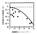
そこで、図1及び図2に測定波長248nm及び193nmでのサンプルの表面粗さと散乱損失を除外した理論透過率の関係を示す。
表面粗さに起因する、表面の散乱損失を除外した理論透過率T(散)は以下の近似式を用いて算出される。
【0024】
【数5】
また、図中に示す種々の表面粗さに対する分光透過率は、透過率測定サンプルに同一条件で製造された合成石英ガラスを用い、表面粗さ以外の規格は平行度30秒、面精度3λ、厚さt=10±0.05mmとした。
尚、表面粗さは光学干渉方式の表面粗さ計を用いて測定し、以下の式で求められる。
【0026】
【数6】
図1及び図2から解る様に、表面散乱損失を含めた理論透過率を計算すると、サンプルの表面粗さの増加に伴い、測定波長の理論透過率、すなわち248nmでは92.12%/cm、193nmでは90.87%/cmからずれる傾向がある。
ここで、図1,2中の波線は表面散乱損失のない場合の理論透過率を示し、実線は、表面粗さに依存した表面散乱を含めた理論透過率を、●ドットは実測定値を示す。
【0028】
そこで、理論上、測定精度を確保するためには表面粗さrms=10Å以下の透過率測定サンプルの規格が必要となることが解る。
以上のことから、本発明は光学素材の透過率の測定方法において、透過率測定サンプルに規格を設け、その規格を平行度30秒以下、面精度を平行度と同程度以下、表面粗さrms=10Å以下とし、内部吸収係数0.1%/cmを有意差として安定に測定することを可能とする。
【0029】
一方、図1及び図2から解る様に、種々の表面粗さに対する分光透過率の実測定値(●ドット)は、大きなばらつきがあるが表面散乱損失を除外した理論透過率と同様な傾向を示す。
しかしながら、分光透過率は表面粗さのみによらず、表面散乱損失を除外した理論透過率より少なくとも0.1%以上低く測定されることが解る。また、この現象は特に、波長の短い193nmで顕著である。
【0030】
また、本発明者らは、分光透過率の低下原因である表面損失が、散乱損失だけでは説明できないことから、サンプル表面の各種測定を行った。
サンプル表面の残留不純物の分析は通常の表面分析方法、例えばESCA、蛍光X線分析装置では、感度の点で問題があり、不純物の定量は不可能であった。そこで、全反射蛍光X線分析装置により分析を行った。結果を以下に示す。
a)分光透過率が特に低く測定されたサンプル表面に多量のCe不純物が検出された。
b)全反射蛍光X線分析法によりCe不純物が検出されない、サンプルでも193nmでの分光透過率が低く測定されることがあった。
【0031】
これは、サンプルを作製する際に使用される研磨剤の主成分であるCeO2がサンプル表面の微小クラック部に残留しているためと考えられる。サンプル表面に残留する不純物としては、光学素材の研磨剤の主成分CeO2、Al2O3、ZrO2及びダイヤモンド砥粒等の他にも研磨剤に含まれている様々な成分が考えられる。これらの成分がサンプル表面に微量の不純物として残留する場合においても同様な表面損失を引き起こすと考えられる。
【0032】
金属不純物の影響はとしては、高純度SiO2微粒子を使用した、仕上げ研磨によって、除去可能である。
また、さらに短波長域では、検出限界以下の有機系の残留物やCe以外の不純物等の影響あるいは残留応力に起因する構造欠陥の影響が大きくなり、b)の結果が得られる事が実験、分析などによりわかってきた。
【0033】
残留応力については、酸もしくはアルカリ洗浄法により除去可能である。
これらの事実から、透過率測定に影響を与える因子として、サンプルの表面散乱以外の原因としては、サンプル表面の吸収による損失の影響が大きいことが判明した。
そこで、本発明者らは光学素材の透過率の測定方法において、内部吸収係数0.1%/cmを有意差として精度良く測定することを可能とする、透過率測定サンプルの作製方法を検討した。その結果、紫外線照射による紫外線洗浄を行うことが有効であることを様々な実験により見い出した。
【0034】
これは、サンプルに紫外線を照射する事で、表面の有機物を分解し発生したオゾンO3で同時に酸化除去する事で、表面の洗浄する方法である。
紫外線洗浄に至った、経緯を以下に記す。
クリ−ンル−ムや清浄度を保ったまま真空封入後N2パージした容器内にサンプルを保管しても、比較的早く透過率測定値が変化し測定に誤差を生じること、及びクリ−ンル−ム内のSi基板の表面汚染現象にヒントを得、放出ガス分析、ESCA、接触角測定等様々な実験を行ったところ、以下の事がわかった。
▲1▼湿式精密洗浄後、時間の経過と共に透過率が減少する。
▲2▼湿式精密洗浄後、時間の経過と共に表面に炭化水素系の不純物が増加する。
【0035】
これらより、透過率低下の原因は、表面に付着した数原子層の炭化水素系不純物による表面損失であると推定される。
これらの対策として、測定直前に、紫外線洗浄を行うことを試してみた。
実験にて確認した結果、紫外線洗浄法は、処理が簡便であり、短時間で極めて効果が高い事が確認できた。この事からも、表面損失の主因として、表層の炭化水素化合物の存在が確認できる。
【0036】
次に、紫外線洗浄による効果の実験結果を詳しく記述する。
紫外線洗浄の原理は、低圧Hgランプ等を用いた紫外線照射による炭水化物などの有機化合物の分解作用と、照射の際、空気中のO2が、O2→O+O、O+O2→O3の反応を経て生成される活性酸素O*の強力な酸化作用により有機化合物がガス状態の物質、例えばH2O、CO2、N2等に変化し、非照射表面より除去され、非常に清浄な表面が得られる事にある。
【0037】
ただし、紫外線処理で除去でき得る、汚染物は表層数原子層である事が望ましい。これは、汚染物による膜厚が厚いと、処理時間が長くなる事がある。この為他の洗浄法、例えば、酸及びアルカリ洗浄、もしくは、水系、有機系を組み合わせたいわゆる精密洗浄法などと組み合わせる事が望ましい。
この効果は、波長がより短い、193nmで顕著であるので、193nm透過率測定について、調査した。
【0038】
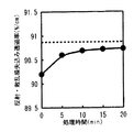
まず、紫外線処理時間と193nmの反射損失込み透過率の関係を調査した。図3に示す様に、処理開始と共に透過率測定値が上昇し、屈折率から計算した理論透過率値90.87%に漸近する。理論値からのズレは、内部散乱による損失である。内部散乱測定値から算出した内部散乱損失係数0.15%/cmを考慮すると内部吸収は0.05%/cm以下と見積もる事が出来る。
【0039】
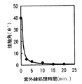
また、紫外線処理時間と接触角の関係を図4に、接触角と表面損失の関係を図5に示す。
ここで、接触角とは、水を使用した液適法により測定した値である。
清浄な表面は、高い表面エネルギ−を持ち、汚染された表面は低い表面エネルギ−を持つため、等量の液滴を滴下すると、清浄な面では大きく広がり接触角は小さく、汚染された面では、滴をはじくため、大きな接触角となる。
【0040】
つまり、接触角が大きいサンプルの表面には、汚染物である有機物が表面に付着しており、紫外線処理により、有機物が除去され、表面損失が減少する。このため、透過率の測定が正確に出来ると思われる。
図4より読みとると、表面損失を0.1%にする為には、接触角を10゜以下にする事により達成できることが確認できた。
【0041】
光源としては、Hgランプ等の紫外域で高出力のランプ、エキシマランプ、ArFエキシマレ−ザ−の様な紫外域パルスレーザ、Arイオンレーザの第2次高調波またはNd:YAG第3次高調波の様な紫外域CWレーザ等が使用できる事を低圧Hgランプ同様の実験にて確認した。
特に、Hgランプを用いた場合は、サンプル自体がダメージを受けてサンプルの物性変化(例えば透過率低下、クラックの発生、表面形状の変化等)を防ぐことができるので、好ましい。
【0042】
紫外線処理の際の、雰囲気O2濃度依存性を確認したところ、5%以上のO2濃度では処理による効果及び処理時間による洗浄効果はほとんど変わらなかった。しかし、5%以下では、処理効果がやや劣り、同じ効果を得るための処理時間が長くなった。このため、紫外線処理時の雰囲気O2濃度は望ましくは5%以上が必要である。
【0043】
この効果は、多成分の光学ガラス、及びCaF2等の光学単結晶等の透過率精密測定にも、適用できる。
以下、実施例により、本発明を詳しく説明する。
【0044】
【実施例】
光学素材である高純度石英ガラスインゴットは、原料として高純度の四塩化ケイ素を用い、石英ガラス製バーナーにて酸素ガス及び水素ガスを混合・燃焼させ、中心部から原料ガスをキャリアガス(通常酸素ガス)で希釈して噴出させ、ターゲット上に堆積、溶融して合成した。これにより、直径180mm、長さ550mmの石英ガラスインゴットを得た。
【0045】
さらに、得られた石英ガラスインゴット及び蛍石単結晶について、含有金属不純物(Ti,Cr,Fe,Ni,Cu,Zn,Co,Mn)の定量分析を誘導結合プラズマ発光分光法によって行ったところ、濃度がそれぞれ20ppb以下であり、本石英ガラス及び蛍石は高純度であることがわかった。
また、この石英ガラスの内部散乱損失係数は、積分球を使用した実測値から
0.15%/cmである事を算出した。ここで、内部散乱の原因は、石英ガラスの本質的な物性に起因する、レ−リ−散乱・ブリリアン散乱等が主因である。
【0046】
透過率測定器は、平行ビ−ムを用いたダブルビ−ム超精密分光光度計を作製し、使用した。
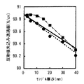
ここで、193nm透過率に関して、平行光でない市販の分光光度計で得たデ−タと、本実施例で作製した超精密分光光度計で得たデ−タの比較を図6に示す。
【0047】
サンプルは全く同一のものを測定し、表面損失は本特許のサンプル作製法を用いたため、事実上無視し得る量である。実線は、内部散乱損失係数0.15%/cmの内部散乱損失分を含んだ、理論透過率である。
●ドットは本特許の超精密分光光度計、■ドットは市販の分光光度計で、透過率のサンプル厚さ依存性を測定した実デ−タである。●ドットの回帰直線は、切片が理論値と一致している事、直線からのズレが小さいのに対して、■ドットはサンプル厚さのによる光路のズレによる、光電子倍増管の光電面の感度むらの影響により、直線性がみられない。本実施例の超精密分光光度計は、平行光を用いているため、精度が非常に良い事が確認された。図6中の●ドットの回帰式と理論値実線のズレは内部吸収によると思われる。この様に、本発明の透過率測定法を用いれば、内部吸収は、透過損失−内部散乱損失により、高精度で算出する事が可能である。
【0048】
以下実施例のデ−タは全て、本発明により作製した平行ビ−ムを用いたダブルビ−ム超精密分光光度計を使用した。
また、使用した石英ガラスサンプルの内部散乱損失係数は、全て0.15%/cm±0.03である。
[実施例1]
透過率サンプルの紫外線洗浄効果を確認した結果を、図7に示す。
【0049】
■ドットは、SiO2で仕上げ研磨し、平行度30秒以下、面精度を平行度と同程度以下、表面粗さrms=10Å以下とした精密研磨後、精密洗浄を行ったサンプルの測定値である。
また、●ドットは、さらに透過率測定前に紫外線洗浄を10分間行ったサンプルのデータである。
【0050】
それぞれ、波線、一点鎖線は、回帰直線であり、決定係数R=0.99、標準誤差=0.01であった。
実線は、内部散乱損失係数を0.15%/cmの内部散乱損失分を含んだ理論透過率(反射・内部散乱損失込み透過率)を示す。
紫外線処理無しのデータの直線性は、本特許による測定装置の精度が高いため良いが、切片が理論値より0.12%低い。これは、傾きが●ドットの回帰直線と同一である事からも、有機系汚染物による表面損失であると判断される。
【0051】
それに対して、紫外線洗浄した、●ドットの測定値は、切片が理論値と一致した。
この様に切片のずれは表面損失を示し、それに対し内部散乱損失を含んだ、理論透過率、測定値の回帰直線など厚さ依存性を示す成分が、内部透過損失である。
[実施例2]
透過率サンプルの作製法と透過率測定装置を使用した測定例を図8を示す。
【0052】
測定に使用した、サンプルはやや吸収が通常より若干大きい事が予測されるものを用いた。
透過率測定サンプルは、SiO2で仕上げ研磨し、平行度30秒以下、面精度を平行度と同程度以下、表面粗さrms=10Å以下とした精密研磨後、精密洗浄を行い、さらに透過率測定前に紫外線洗浄を10分間行ったサンプルの透過率測定データである。
【0053】
実線は、内部散乱損失係数0.15%/cmの内部散乱損失分を含んだ理論透過率(反射・内部散乱損失込み透過率)を示す。
破線は、回帰直線であり、決定係数R=0.99、標準誤差=0.01であった。非常に直線性が高い事及び切片が実線と一致、つまり理論値と一致している事がわかる。回帰直線の傾きから、透過損失係数0.19%/cmを算出した。透過損失係数−内部散乱損失係数=吸収係数であるから、0.19−0.15=0.04%/cmを求めた。
[実施例3]
透過率サンプルの作製法と透過率測定装置を使用した測定例を図9を示す。
【0054】
測定に使用した、サンプルはやや吸収が平均的である事が予測されるものを用いた。
透過率測定サンプルは、SiO2で仕上げ研磨し、平行度30秒以下、面精度を平行度と同程度以下、表面粗さrms=10Å以下とした精密研磨後、精密洗浄を行い、さらに透過率測定前に紫外線洗浄を10分間行ったサンプルの透過率測定データである。
【0055】
実線は、内部散乱損失係数0.15%/cmの内部散乱損失分を含んだ理論透過率(反射・内部散乱損失込み透過率)を示す。
波線は、回帰直線であり、決定係数R=0.99、標準誤差=0.01であった。非常に直線性が高い事及び切片が実線と一致、つまり理論値と一致している事がわかる。回帰直線の傾きから、透過損失係数0.17%/cmを算出した。透過損失係数ー内部散乱損失係数=吸収係数であるから、0.17−0.15=0.02%/cmを求めた。
【0056】
【発明の効果】
本発明によるサンプルの規格及びサンプルの作製方法により、光学素材の内部透過率を±0.1%/cm以下の誤差で高精度に測定することが可能となった。本発明は、短波長域の紫外域及び真空紫外域の透過率測定において特に有効である。
【0057】
また、短波長域の微少な吸収が問題となる光学部品にも利用可能である。
【図面の簡単な説明】
【図1】サンプルの表面粗さと種々の透過率(248nm)の関係をプロットしたグラフである。
【図2】サンプルの表面粗さと種々の透過率(193nm)の関係をプロットしたグラフである。
【図3】サンプル紫外線処理時間と分光透過率(193nm)の関係をプロットしたグラフである。
【図4】サンプル紫外線処理時間とサンプル表面接触角の関係をプロットしたグラフである。
【図5】サンプル表面接触角と表面損失(193nm)の関係をプロットしたグラフである。
【図6】本発明による超精密透過率測定装置の透過率測定におけるサンプル厚さ依存性を示したグラフである。
【図7】本発明による実施例1、合成石英ガラスの193nm分光透過率測定結果をプロットしたグラフである。
【図8】本発明による実施例2、合成石英ガラスの193nm分光透過率測定結果をプロットしたグラフである。
【図9】本発明による実施例3、合成石英ガラスの193nm分光透過率測定結果をプロットしたグラフである。[0001]
[Industrial applications]
The present invention relates to a sample used for highly accurate measurement of the transmittance of an optical material, for example, a multi-component optical glass, a synthetic quartz glass, a crystal material, and the like, for example, an internal transmittance (spectral transmittance not including reflection loss), and a method for producing the sample. It relates to a measuring method. In particular, multi-component optical glass used in visible / ultraviolet optical systems represented by g-line (436 nm) and i-line (365 nm) lithography, and 300 nm or less such as KrF (248 nm) and ArF (193 nm) excimer laser lithography The present invention relates to a synthetic quartz glass and a transmittance measurement sample of a crystal material used in the ultraviolet optical system.
[0002]
[Prior art]
2. Description of the Related Art Conventionally, in an optical lithography technique for exposing and transferring a fine pattern of an integrated circuit onto a wafer such as silicon, an exposure apparatus called a stepper is used.
The light source of this stepper has been shortened in wavelength from g-line to i-line with the recent high integration of LSI. The internal transmittance of the optical glass used for the illumination system of such a stepper or the projection lens is 99.8% / cm or 99.9% / cm or more (internal absorption 0.2% / cm or 0.1%). % / Cm or less). With the further increase in the degree of integration of LSIs, the light source of the stepper has shifted to KrF or ArF excimer laser. General optical glass can no longer be used for the illumination system or projection lens of such an excimer laser stepper, and is limited to materials such as quartz glass and fluorite. The internal transmittance of silica glass and fluorite used for the illumination system or projection lens of such an excimer laser stepper is required to be 99.8% / cm or 99.9% / cm or more. Therefore, development is being pursued to increase the transmittance of the optical material in the ultraviolet light region. On the other hand, as the wavelength becomes shorter, it is technically very difficult to measure the internal transmittance of the optical material with high accuracy. Therefore, in order to achieve a high transmittance of the optical material, first, the internal transmittance (0.1% of internal absorption) of an optical glass, a synthetic quartz glass, a crystal material or the like having only such a weak absorption exists. / Cm) is indispensable.
[0003]
[Problems to be solved by the invention]
As a method for measuring the internal transmittance, a method for measuring the internal transmittance of the optical glass is specified in JOGIS-17-82 of the Japan Optical Glass Industrial Standards. For other optical materials such as quartz glass and crystalline materials, the method of measuring the internal transmittance is similar to this. In this specification, for the preparation of the transmittance measurement sample, a pair of 3 mm and 10 mm in thickness was used, and both faces were polished in parallel, and the internal transmittance was indicated by a value for a 10 mm thick glass. Due to the indication and rounding off to three decimal places, the measurement accuracy is only 1% / cm of internal absorption, and especially the problem of measurement error of internal transmittance becomes significant, i-line, excimer laser, etc. Was not targeted.
[0004]
In the method of measuring the transmittance of an optical material, the following items are mainly examined in order to measure the internal absorption at 0.1% / cm as a significant difference.
(1) Spectral transmittance (transmittance including reflection loss) is measured using a spectrophotometer having high basic performance.
{Circle around (2)} In a commercially available spectrophotometer, a transmittance shift caused by an optical path shift caused by inserting a sample into a measurement optical path is corrected.
(3) A sample with high accuracy, that is, a sample with few measurement errors is produced.
[0005]
Regarding (1) and (2), the measurement fluctuation at 193 nm and 248 nm achieved ± 0.01% in 3σ due to the development of the device.
In addition, an apparatus was manufactured in which the influence of sensitivity unevenness of the photocathode of a photomultiplier used as a detector, which is caused by the deviation of the optical path due to refraction due to parallel rays, is substantially eliminated.
[0006]
However, regarding (3), there has been no standard for a transmittance measurement sample, and the items and the degree defining the accuracy of the sample have not been quantified. Therefore, a production method for realizing the standard of the transmittance measurement sample has not been described.
[0007]
[Means for Solving the Problems]
The present inventors have intensively studied, in a method of measuring the transmittance of an optical material, a measurement error caused by a standard and a manufacturing method of a transmittance measurement sample.
Then, as a result of examining the measurement error element caused by the sample, it was found that the parallelism, the surface accuracy, and the surface roughness of the polished surface of the sample became problems.
[0008]
In general, a sample is prepared by cutting a part of an optical material to be evaluated into a shape that can enter a sample chamber of a spectrophotometer, and optically polishing two opposite surfaces in a thickness direction with a commercially available abrasive.
Here, the parallelism is an inclination (angle) with respect to one of two opposing surfaces of the optically polished surface with respect to the reference surface. The surface accuracy is the amount of deviation of the polished surface from the flat prototype, and the surface roughness is the height of irregularities on each optical polished surface.
[0009]
The present inventors previously set the internal transmittance of the optical material to ± 0.1 by using a sample having a parallelism of 30 seconds or less, a surface accuracy of the same degree or less as the parallelism, and a surface roughness rms of 10 ° or less. It is proposed that the measurement can be performed with high accuracy with an error of less than%.
Furthermore, it was found that structural defects caused by residual impurities such as cutting and polishing agents used in preparing the transmittance measurement sample and residual stress caused by processing were causes of a decrease in the spectral transmittance of the optical material. In the preparation of a material sample, a transmittance measurement sample characterized by pre-polishing the sample to a surface roughness rms = about 10 ° and then reducing the rms to 10 ° or less with a SiO 2 abrasive, or performing an acid or alkali treatment. A fabrication method was proposed.
[0010]
However, for example, in the measurement of the transmittance of an optical material in a short wavelength ultraviolet region or a vacuum ultraviolet region, higher precision measurement is desired.
Therefore, further research was conducted on the fact that the surface condition of the transmittance measurement sample greatly affects the measurement accuracy.
The state of the sample surface is governed by three of the above-mentioned factors, in particular, surface roughness, residual impurities such as abrasives, and structural defects caused by residual stress generated by processing. Therefore, by setting the surface loss of the sample to 0.1% or less, measurement with even higher precision became possible.
[0011]
Furthermore, by performing ultraviolet cleaning before the measurement, it was possible to suppress the influence on the measurement result of the sample surface.
[0012]
[Action]
The following equation holds for the optical path shift of the measurement light that affects the parallelism and transmittance of the sample.
[0013]
(Equation 1)
From this, it is understood that it is necessary to define the parallelism of the sample when performing relative comparison of the transmittance. Further, since the direction of inclination of the sample with respect to the measurement light determines the direction of displacement of the measurement light on the detector, it is preferable that the direction of inclination of the sample is preferably aligned during measurement. However, it was found from the experimental results that the measurement error could be ignored if the parallelism was set to 30 seconds or less.
[0015]
The surface accuracy was measured using a fringe scanning interferometer.
The surface accuracy that gives a height difference equivalent to the parallelism (30 seconds) of the sample specified above can be obtained from the following equation.
[0016]
(Equation 2)
Here, λ is the wavelength of the measurement light, usually 546 nm, 2 is the number of surfaces, and L is the maximum length (cm) of the polished surface of the sample, such as the diameter of the sample and the diagonal line. Therefore, a surface accuracy of 1.33 Lλ or less is required. It was found that there was no problem in the measurement accuracy if the measured value of the surface accuracy of the transmittance measurement sample was within the surface accuracy derived by the above equation. When d is obtained from the above equation, d = 1.33L.
[0018]
Regarding the surface roughness, a verification experiment of sample specifications was conducted, paying particular attention to the fact that the spectral transmittance of the optical material is measured lower than the theoretical transmittance calculated from the refractive index. Here is an example.
First, the theoretical transmittance will be described. The spectral transmittance T considering the multiple reflection is defined by the following equations (1) and (2).
[0019]
(Equation 3)
R is the reflectance when the measuring light is incident perpendicularly to the surface of the optical material.
[0021]
(Equation 4)
The theoretical transmittance T 0 is the calculated value of the spectral transmittance when the reduction of the light amount is only the reflection loss in the equation (1), that is, the internal absorption coefficient a is 0, or the spectral transmittance when the sample thickness is infinitely small. It is a calculated value of the rate.
Generally, the spectral transmittance is measured lower than the theoretical transmittance, that is, the scattering loss due to the surface roughness of the sample is considered as one of the causes of the surface loss of the measured light amount.
[0023]
1 and 2 show the relationship between the surface roughness of the sample at the measurement wavelengths of 248 nm and 193 nm and the theoretical transmittance excluding the scattering loss.
The theoretical transmittance T (scatter) excluding the scattering loss of the surface due to the surface roughness is calculated using the following approximate expression.
[0024]
(Equation 5)
Further, the spectral transmittance for various surface roughness shown in the figure, the synthetic quartz glass manufactured under the same conditions as the transmittance measurement sample, the standard other than the surface roughness is parallelism 30 seconds, surface accuracy 3λ, The thickness t was 10 ± 0.05 mm.
The surface roughness is measured using an optical interference type surface roughness meter, and can be obtained by the following equation.
[0026]
(Equation 6)
As can be understood from FIGS. 1 and 2, the theoretical transmittance including the surface scattering loss is calculated. As the surface roughness of the sample increases, the theoretical transmittance at the measurement wavelength, that is, 92.12% / cm at 248 nm, At 193 nm, there is a tendency to deviate from 90.87% / cm.
Here, the wavy lines in FIGS. 1 and 2 indicate the theoretical transmittance without surface scattering loss, the solid line indicates the theoretical transmittance including surface scattering depending on the surface roughness, and the dot indicates the actual measured value. .
[0028]
Therefore, it is theoretically understood that a standard of a transmittance measurement sample having a surface roughness rms = 10 ° or less is required in order to secure measurement accuracy.
In view of the above, the present invention provides a method for measuring the transmittance of an optical material, in which a standard is set for a transmittance measurement sample, the standard is set to a parallelism of 30 seconds or less, the surface accuracy is equal to or less than the parallelism, and the surface roughness rms. = 10 ° or less, making it possible to stably measure the internal absorption coefficient 0.1% / cm as a significant difference.
[0029]
On the other hand, as can be seen from FIGS. 1 and 2, the actual measured values of the spectral transmittance for various surface roughnesses (dots) show a similar tendency to the theoretical transmittance excluding surface scattering loss, although there is a large variation. .
However, it is understood that the spectral transmittance is measured not only by the surface roughness but also by at least 0.1% lower than the theoretical transmittance excluding the surface scattering loss. This phenomenon is particularly remarkable at a short wavelength of 193 nm.
[0030]
In addition, the present inventors performed various measurements on the sample surface because the surface loss, which is the cause of the decrease in spectral transmittance, cannot be explained only by the scattering loss.
The analysis of the residual impurities on the sample surface has a problem in sensitivity with a normal surface analysis method, for example, ESCA and X-ray fluorescence spectrometer, and it is impossible to quantify the impurities. Therefore, analysis was performed by a total reflection X-ray fluorescence analyzer. The results are shown below.
a) A large amount of Ce impurity was detected on the sample surface where the spectral transmittance was measured particularly low.
b) In some samples, Ce impurities were not detected by the total reflection X-ray fluorescence spectroscopy, and the sample had a low spectral transmittance at 193 nm.
[0031]
This is presumably because CeO 2, which is the main component of the abrasive used when preparing the sample, remains in the minute cracks on the sample surface. As the impurities remaining on the sample surface, there can be considered various components contained in the polishing agent in addition to the main components CeO 2 , Al 2 O 3 , ZrO 2 and diamond abrasive grains of the polishing agent for the optical material. It is thought that the same surface loss is caused even when these components remain as trace impurities on the sample surface.
[0032]
The effect of metal impurities can be removed by finish polishing using high-purity SiO 2 fine particles.
Further, in the short wavelength region, the effects of organic residues below the detection limit, impurities other than Ce, and the like, and the effects of structural defects caused by residual stress are increased, and the results of b) can be obtained by experiments and experiments. It became clear by analysis.
[0033]
The residual stress can be removed by an acid or alkali cleaning method.
From these facts, it was found that the factor other than the surface scattering of the sample as a factor affecting the transmittance measurement was greatly affected by the loss due to absorption of the sample surface.
Therefore, the present inventors have studied a method for measuring a transmittance of an optical material, which is a method of measuring a transmittance, which enables accurate measurement with an internal absorption coefficient of 0.1% / cm as a significant difference. . As a result, it has been found through various experiments that it is effective to perform ultraviolet cleaning by ultraviolet irradiation.
[0034]
This is a method of cleaning the surface by irradiating the sample with ultraviolet rays to decompose organic substances on the surface and oxidize and remove the ozone O 3 at the same time.
The process that led to the UV cleaning is described below.
Chestnut - Nru - be stored samples in a container was vacuum sealed after N 2 purge while maintaining the arm and cleanliness, causing an error to relatively quickly transmittance measured value changes measured, and chestnut - Nru Inspired by the surface contamination phenomena of the Si substrate in the system, various experiments such as emission gas analysis, ESCA, and contact angle measurement were performed, and the following was found.
{Circle around (1)} After the wet precision cleaning, the transmittance decreases with time.
{Circle over (2)} After the wet precision cleaning, hydrocarbon-based impurities increase on the surface over time.
[0035]
From these, it is presumed that the cause of the decrease in transmittance is surface loss due to hydrocarbon impurities in several atomic layers attached to the surface.
As a countermeasure for these, an attempt was made to perform ultraviolet cleaning immediately before the measurement.
As a result of an experiment, it was confirmed that the ultraviolet cleaning method was easy to carry out and was extremely effective in a short time. This also confirms the presence of hydrocarbon compounds in the surface layer as the main cause of the surface loss.
[0036]
Next, the experimental results of the effect of the ultraviolet cleaning will be described in detail.
The principle of ultraviolet cleaning is that the decomposition of organic compounds such as carbohydrates by ultraviolet irradiation using a low-pressure Hg lamp or the like, and that the O 2 in the air, upon irradiation, causes the reaction of O 2 → O + O and O + O 2 → O 3 The organic compound changes into a gaseous substance, for example, H 2 O, CO 2 , N 2, etc. by the strong oxidizing action of the active oxygen O * generated through the reaction, and is removed from the non-irradiated surface. To be obtained.
[0037]
However, it is desirable that contaminants that can be removed by ultraviolet treatment be a few atomic layers on the surface. This is because when the film thickness due to contaminants is large, the processing time may be long. For this reason, it is desirable to combine it with another cleaning method, for example, an acid and alkali cleaning method, or a so-called precision cleaning method combining an aqueous system and an organic system.
Since this effect is more pronounced at shorter wavelengths, 193 nm, 193 nm transmission measurements were investigated.
[0038]
First, the relationship between the ultraviolet treatment time and the transmittance including the reflection loss at 193 nm was investigated. As shown in FIG. 3, the measured transmittance value increases with the start of the treatment, and approaches the theoretical transmittance value of 90.87% calculated from the refractive index. The deviation from the theoretical value is a loss due to internal scattering. Considering the internal scattering loss coefficient 0.15% / cm calculated from the measured internal scattering value, the internal absorption can be estimated to be 0.05% / cm or less.
[0039]
FIG. 4 shows the relationship between the UV treatment time and the contact angle, and FIG. 5 shows the relationship between the contact angle and the surface loss.
Here, the contact angle is a value measured by a liquid method using water.
A clean surface has a high surface energy, and a contaminated surface has a low surface energy. , Repels the droplet, resulting in a large contact angle.
[0040]
That is, on the surface of the sample having a large contact angle, an organic substance as a contaminant adheres to the surface. The organic substance is removed by the ultraviolet treatment, and the surface loss is reduced. Therefore, it is considered that the transmittance can be measured accurately.
It was confirmed from FIG. 4 that the surface loss can be reduced to 0.1% by setting the contact angle to 10 ° or less.
[0041]
The light source may be a high-output lamp in the ultraviolet region such as an Hg lamp, an excimer lamp, an ultraviolet pulse laser such as an ArF excimer laser, a second harmonic of an Ar ion laser, or a third harmonic of Nd: YAG. It was confirmed by an experiment similar to that of a low-pressure Hg lamp that an ultraviolet CW laser or the like as described above can be used.
In particular, the use of an Hg lamp is preferable because the sample itself can be damaged to prevent a change in physical properties of the sample (for example, a decrease in transmittance, generation of cracks, change in surface shape, and the like).
[0042]
When the dependence on the atmosphere O 2 concentration during the ultraviolet treatment was confirmed, the effect by the treatment and the cleaning effect by the treatment time hardly changed when the O 2 concentration was 5% or more. However, at 5% or less, the processing effect was slightly inferior, and the processing time for obtaining the same effect was prolonged. For this reason, the atmosphere O 2 concentration at the time of the ultraviolet treatment is desirably 5% or more.
[0043]
This effect can also be applied to the multi-component optical glass and the transmittance precision measurement of an optical single crystal such as CaF 2 .
Hereinafter, the present invention will be described in detail with reference to examples.
[0044]
【Example】
The high-purity quartz glass ingot, which is an optical material, uses high-purity silicon tetrachloride as a raw material, mixes and burns oxygen gas and hydrogen gas with a burner made of quartz glass, and transfers the raw material gas from the center to a carrier gas (usually oxygen). Gas) and ejected, deposited on the target, melted and synthesized. Thus, a quartz glass ingot having a diameter of 180 mm and a length of 550 mm was obtained.
[0045]
Furthermore, the obtained quartz glass ingot and fluorite single crystal were subjected to inductively coupled plasma emission spectroscopy for quantitative analysis of contained metal impurities (Ti, Cr, Fe, Ni, Cu, Zn, Co, Mn). The respective concentrations were 20 ppb or less, indicating that the present quartz glass and fluorite were of high purity.
Further, the internal scattering loss coefficient of this quartz glass was calculated to be 0.15% / cm from an actually measured value using an integrating sphere. Here, the main cause of internal scattering is Rayleigh scattering, Brillian scattering, and the like, which are caused by the intrinsic physical properties of quartz glass.
[0046]
As a transmittance meter, a double beam ultra-precision spectrophotometer using a parallel beam was prepared and used.
FIG. 6 shows a comparison of data obtained with a commercially available spectrophotometer that is not parallel light and data obtained with the ultra-precision spectrophotometer manufactured in this example, for the 193 nm transmittance.
[0047]
The samples were measured exactly the same, and the surface loss was virtually negligible due to the use of the sample preparation method of this patent. The solid line is the theoretical transmittance including the internal scattering loss coefficient of 0.15% / cm.
The dot is the actual data obtained by measuring the dependence of the transmittance on the sample thickness using the ultra-precision spectrophotometer of this patent, and the dot is the commercially available spectrophotometer. ● The regression line of the dot is that the intercept is consistent with the theoretical value and the deviation from the line is small, while the dot is the sensitivity of the photomultiplier tube's photocathode due to the deviation of the optical path due to the sample thickness. No linearity is observed due to unevenness. Since the ultra-precision spectrophotometer of this example uses parallel light, it was confirmed that the accuracy was very good. The deviation between the regression equation of the dot and the theoretical solid line in FIG. 6 seems to be due to internal absorption. As described above, if the transmittance measurement method of the present invention is used, the internal absorption can be calculated with high accuracy by the transmission loss-the internal scattering loss.
[0048]
Hereinafter, all the data in the examples used a double beam ultra-precision spectrophotometer using a parallel beam manufactured according to the present invention.
Further, the internal scattering loss coefficients of the quartz glass samples used are all 0.15% / cm ± 0.03.
[Example 1]
FIG. 7 shows the result of confirming the ultraviolet light cleaning effect of the transmittance sample.
[0049]
(2) Dots are measured values of a sample that has been precision polished after finish polishing with SiO2, parallelism of 30 seconds or less, surface precision of the same degree or less as parallelism, and surface roughness rms of 10 ° or less, and then precision cleaning. .
In addition, the dot indicates data of a sample that was further subjected to ultraviolet cleaning for 10 minutes before transmittance measurement.
[0050]
The wavy line and the one-dot chain line are regression lines, respectively, and the coefficient of determination R was 0.99 and the standard error was 0.01.
The solid line indicates the theoretical transmittance (the transmittance including reflection and internal scattering loss) including the internal scattering loss coefficient of 0.15% / cm.
The linearity of the data without UV treatment is good due to the high accuracy of the measuring device according to the present invention, but the intercept is 0.12% lower than the theoretical value. This is also determined to be surface loss due to organic contaminants since the slope is the same as the regression line of the dot.
[0051]
On the other hand, the measured value of the dot, which was washed with ultraviolet rays, was the same as the theoretical value in the intercept.
As described above, the displacement of the intercept indicates the surface loss, whereas the component showing the thickness dependence, such as the theoretical transmittance and the regression line of the measured value, including the internal scattering loss, is the internal transmission loss.
[Example 2]
FIG. 8 shows a method of preparing a transmittance sample and a measurement example using a transmittance measurement device.
[0052]
The sample used for the measurement was one whose absorption was expected to be slightly larger than usual.
The transmittance measurement sample is finish-polished with SiO 2 , precision-polished to have a parallelism of 30 seconds or less, surface precision equal to or less than the parallelism, and surface roughness rms = 10 ° or less, and then precision-cleaned. It is the transmittance | permeability measurement data of the sample which performed ultraviolet washing for 10 minutes before the measurement.
[0053]
The solid line indicates the theoretical transmittance (the transmittance including reflection and internal scattering loss) including the internal scattering loss coefficient of 0.15% / cm.
The broken line is the regression line, and the coefficient of determination R = 0.99 and the standard error = 0.01. It can be seen that the linearity is very high and the intercept matches the solid line, that is, matches the theoretical value. From the slope of the regression line, a transmission loss coefficient of 0.19% / cm was calculated. Since transmission loss coefficient−internal scattering loss coefficient = absorption coefficient, 0.19−0.15 = 0.04% / cm was determined.
[Example 3]
FIG. 9 shows a method for preparing a transmittance sample and a measurement example using a transmittance measurement device.
[0054]
The sample used for the measurement used was expected to have a somewhat average absorption.
The transmittance measurement sample is finish-polished with SiO 2 , precision-polished to have a parallelism of 30 seconds or less, surface precision equal to or less than the parallelism, and surface roughness rms = 10 ° or less, and then precision-cleaned. It is the transmittance | permeability measurement data of the sample which performed ultraviolet washing for 10 minutes before the measurement.
[0055]
The solid line indicates the theoretical transmittance (the transmittance including reflection and internal scattering loss) including the internal scattering loss coefficient of 0.15% / cm.
The wavy line is a regression line, and the coefficient of determination R = 0.99 and the standard error = 0.01. It can be seen that the linearity is very high and the intercept matches the solid line, that is, matches the theoretical value. From the slope of the regression line, a transmission loss coefficient of 0.17% / cm was calculated. Since transmission loss coefficient-internal scattering loss coefficient = absorption coefficient, 0.17-0.15 = 0.02% / cm was determined.
[0056]
【The invention's effect】
According to the sample standard and the sample manufacturing method of the present invention, the internal transmittance of the optical material can be measured with high accuracy with an error of ± 0.1% / cm or less. INDUSTRIAL APPLICABILITY The present invention is particularly effective in measuring transmittance in the ultraviolet region in the short wavelength region and in the vacuum ultraviolet region.
[0057]
Further, the present invention can also be used for optical components in which minute absorption in a short wavelength region poses a problem.
[Brief description of the drawings]
FIG. 1 is a graph plotting the relationship between the surface roughness of a sample and various transmittances (248 nm).
FIG. 2 is a graph plotting the relationship between the surface roughness of a sample and various transmittances (193 nm).
FIG. 3 is a graph plotting a relationship between a sample ultraviolet treatment time and a spectral transmittance (193 nm).
FIG. 4 is a graph plotting a relationship between a sample ultraviolet treatment time and a sample surface contact angle.
FIG. 5 is a graph plotting a relationship between a sample surface contact angle and a surface loss (193 nm).
FIG. 6 is a graph showing sample thickness dependence in transmittance measurement of the ultra-precision transmittance measurement device according to the present invention.
FIG. 7 is a graph plotting the measurement results of the 193 nm spectral transmittance of the synthetic quartz glass in Example 1 according to the present invention.
FIG. 8 is a graph plotting the results of measuring the spectral transmittance of a synthetic quartz glass according to Example 2 of the present invention at 193 nm.
FIG. 9 is a graph plotting the measurement results of the 193 nm spectral transmittance of the synthetic quartz glass in Example 3 according to the present invention.
Claims (4)
各研磨面の測定波長の表面損失が0.1%以下であることを特徴とする透過率測定サンプル。In the transmittance measurement sample of the optical material whose opposite two surfaces have been polished,
A transmittance measurement sample characterized in that the surface loss at the measurement wavelength of each polished surface is 0.1% or less.
Priority Applications (1)
| Application Number | Priority Date | Filing Date | Title |
|---|---|---|---|
| JP07017395A JP3572425B2 (en) | 1995-03-28 | 1995-03-28 | Sample for measuring transmittance, method for preparing the sample, and method for measuring transmittance |
Applications Claiming Priority (1)
| Application Number | Priority Date | Filing Date | Title |
|---|---|---|---|
| JP07017395A JP3572425B2 (en) | 1995-03-28 | 1995-03-28 | Sample for measuring transmittance, method for preparing the sample, and method for measuring transmittance |
Publications (2)
| Publication Number | Publication Date |
|---|---|
| JPH08271393A JPH08271393A (en) | 1996-10-18 |
| JP3572425B2 true JP3572425B2 (en) | 2004-10-06 |
Family
ID=13423882
Family Applications (1)
| Application Number | Title | Priority Date | Filing Date |
|---|---|---|---|
| JP07017395A Expired - Lifetime JP3572425B2 (en) | 1995-03-28 | 1995-03-28 | Sample for measuring transmittance, method for preparing the sample, and method for measuring transmittance |
Country Status (1)
| Country | Link |
|---|---|
| JP (1) | JP3572425B2 (en) |
Families Citing this family (2)
| Publication number | Priority date | Publication date | Assignee | Title |
|---|---|---|---|---|
| JP4701469B2 (en) * | 1999-03-25 | 2011-06-15 | 旭硝子株式会社 | Method for producing synthetic quartz glass for optical member |
| JP4051474B2 (en) | 1999-04-01 | 2008-02-27 | 株式会社ニコン | Method for measuring transmittance of optical member for ultraviolet |
-
1995
- 1995-03-28 JP JP07017395A patent/JP3572425B2/en not_active Expired - Lifetime
Also Published As
| Publication number | Publication date |
|---|---|
| JPH08271393A (en) | 1996-10-18 |
Similar Documents
| Publication | Publication Date | Title |
|---|---|---|
| KR101409682B1 (en) | Method of finishing the surface of preliminarily polished glass substrate | |
| EP1240556B1 (en) | Photolithography method, photolithography mask blanks, and method of making | |
| CZ378297A3 (en) | Removal of material by polarized radiation and due to the action of radiation on the bottom side | |
| TW201719275A (en) | Substrate base substrate, substrate with multilayer reflective film, transmissive reticle base, reflective reticle base, transmissive reticle, reflective reticle, and semiconductor device manufacturing method | |
| JP3669378B2 (en) | Optical material and manufacturing method thereof | |
| JP4104338B2 (en) | Synthetic quartz glass material for ArF exposure equipment | |
| US5983672A (en) | Method for manufacturing optical components for use in the ultraviolet region | |
| JP3125630B2 (en) | Method for producing quartz glass for vacuum ultraviolet and quartz glass optical member | |
| US7635544B2 (en) | Transparent substrate for mask blank and mask blank | |
| JP3572425B2 (en) | Sample for measuring transmittance, method for preparing the sample, and method for measuring transmittance | |
| JP4051474B2 (en) | Method for measuring transmittance of optical member for ultraviolet | |
| TWI853327B (en) | Blank mask, photomask using the same and method of manufacturing semiconductor device | |
| JP3654500B2 (en) | Quartz glass material and optical member for F2 excimer laser optical member | |
| JP4032462B2 (en) | UV optics | |
| JP2970330B2 (en) | Method for measuring internal transmittance and adjusting spectrophotometer | |
| JP3627396B2 (en) | Method and apparatus for measuring internal absorption coefficient of synthetic quartz glass | |
| JPH1187808A (en) | Method for manufacturing optical element for ArF excimer laser | |
| JP4650460B2 (en) | Method for manufacturing ultraviolet optical element | |
| TWI693198B (en) | Method for preparing synthetic quartz glass substrate | |
| JP4321163B2 (en) | Exposure master, exposure master inspection method and exposure method | |
| Sugiyama et al. | Development of EUVL mask blank in AGC | |
| JPH0825773B2 (en) | Manufacturing body of laser optical system | |
| WO2003080525A1 (en) | Synthetic quartz glass member and process for producing the same | |
| JP4701469B2 (en) | Method for producing synthetic quartz glass for optical member | |
| Itakura et al. | Evaluation of characteristics of VUV optical materials irradiated by F2 laser |
Legal Events
| Date | Code | Title | Description |
|---|---|---|---|
| A131 | Notification of reasons for refusal |
Free format text: JAPANESE INTERMEDIATE CODE: A131 Effective date: 20040217 |
|
| A521 | Written amendment |
Free format text: JAPANESE INTERMEDIATE CODE: A523 Effective date: 20040413 |
|
| TRDD | Decision of grant or rejection written | ||
| A01 | Written decision to grant a patent or to grant a registration (utility model) |
Free format text: JAPANESE INTERMEDIATE CODE: A01 Effective date: 20040601 |
|
| A61 | First payment of annual fees (during grant procedure) |
Free format text: JAPANESE INTERMEDIATE CODE: A61 Effective date: 20040614 |
|
| R154 | Certificate of patent or utility model (reissue) |
Free format text: JAPANESE INTERMEDIATE CODE: R154 |
|
| FPAY | Renewal fee payment (event date is renewal date of database) |
Free format text: PAYMENT UNTIL: 20070709 Year of fee payment: 3 |
|
| FPAY | Renewal fee payment (event date is renewal date of database) |
Free format text: PAYMENT UNTIL: 20100709 Year of fee payment: 6 |
|
| FPAY | Renewal fee payment (event date is renewal date of database) |
Free format text: PAYMENT UNTIL: 20100709 Year of fee payment: 6 |
|
| FPAY | Renewal fee payment (event date is renewal date of database) |
Free format text: PAYMENT UNTIL: 20150709 Year of fee payment: 11 |
|
| EXPY | Cancellation because of completion of term |