JP3575813B2 - Semiconductor manufacturing condition indicating device - Google Patents
Semiconductor manufacturing condition indicating device Download PDFInfo
- Publication number
- JP3575813B2 JP3575813B2 JP5370893A JP5370893A JP3575813B2 JP 3575813 B2 JP3575813 B2 JP 3575813B2 JP 5370893 A JP5370893 A JP 5370893A JP 5370893 A JP5370893 A JP 5370893A JP 3575813 B2 JP3575813 B2 JP 3575813B2
- Authority
- JP
- Japan
- Prior art keywords
- manufacturing
- computer
- conditions
- equipment
- input
- Prior art date
- Legal status (The legal status is an assumption and is not a legal conclusion. Google has not performed a legal analysis and makes no representation as to the accuracy of the status listed.)
- Expired - Fee Related
Links
- 238000004519 manufacturing process Methods 0.000 title claims description 84
- 239000004065 semiconductor Substances 0.000 title claims description 21
- 238000000034 method Methods 0.000 claims description 32
- 230000008569 process Effects 0.000 claims description 31
- 238000007726 management method Methods 0.000 description 10
- 238000010586 diagram Methods 0.000 description 9
- 238000004891 communication Methods 0.000 description 8
- 235000012431 wafers Nutrition 0.000 description 6
- 230000006870 function Effects 0.000 description 5
- 238000012545 processing Methods 0.000 description 5
- 230000008859 change Effects 0.000 description 4
- 238000005516 engineering process Methods 0.000 description 3
- 239000010408 film Substances 0.000 description 3
- 238000005468 ion implantation Methods 0.000 description 3
- 230000000694 effects Effects 0.000 description 2
- 238000005530 etching Methods 0.000 description 2
- 239000012535 impurity Substances 0.000 description 2
- 238000000206 photolithography Methods 0.000 description 2
- 230000004044 response Effects 0.000 description 2
- 238000004544 sputter deposition Methods 0.000 description 2
- 238000003860 storage Methods 0.000 description 2
- 239000010409 thin film Substances 0.000 description 2
- 230000005856 abnormality Effects 0.000 description 1
- 238000009825 accumulation Methods 0.000 description 1
- 230000009471 action Effects 0.000 description 1
- 238000004458 analytical method Methods 0.000 description 1
- 238000004380 ashing Methods 0.000 description 1
- 230000008901 benefit Effects 0.000 description 1
- 230000005540 biological transmission Effects 0.000 description 1
- 239000003990 capacitor Substances 0.000 description 1
- 238000013523 data management Methods 0.000 description 1
- 230000007547 defect Effects 0.000 description 1
- 230000002950 deficient Effects 0.000 description 1
- 238000011161 development Methods 0.000 description 1
- 239000000428 dust Substances 0.000 description 1
- 230000001747 exhibiting effect Effects 0.000 description 1
- 239000004973 liquid crystal related substance Substances 0.000 description 1
- 238000012423 maintenance Methods 0.000 description 1
- 239000013077 target material Substances 0.000 description 1
Images
Landscapes
- General Factory Administration (AREA)
- Multi-Process Working Machines And Systems (AREA)
- Management, Administration, Business Operations System, And Electronic Commerce (AREA)
Description
【0001】
【産業上の利用分野】
本発明は半導体の製造に係わり、特に作業時の製造条件の指示に好適な指示方法および指示装置に関する。
【0002】
【従来の技術】
半導体は、ユーザニーズの多様化に伴い、従来のメモリ単一生産ではなく、ニーズにあった製品を多種生産する傾向がある。また、デバイスの微細化のに対応し製造工程での多種製造設備の製造条件も多岐に渡ると供にその製造条件の管理限界も極めて狭い範囲に限定している。このため多品種の製品を迅速に正確に製造するには、製造工程毎に製造ロットの条件を指示し作業を行うことが必要である。この指示を行うシステムとして、例えば「電子情報通信学会論文誌 C Vol.J70−C No.6 」(1987年6 月)第767 頁から第775 頁の「VLSI開発におけるウェーハ処理管理システム」がある。このシステムでは、上記した課題に対して3.5 インチのフロッピーディスクに半導体のウェーハ処理仕様を製造前にあらかじめ登録しておき、半導体の製造工程に合わせて条件の指示を行い、生産するシステムである。この方式では、フロッピーディスクに製造ロットの製造工程、および製造条件が記録されているため、フロッピーディスクと該ディスクをリード/ライトできる計算機があれば生産できることで、データの信頼性を確保している。また、これらより上位の計算機システムがなくも生産できる分散型のシステムとなっている。
【0003】
【発明が解決しようとする課題】
しかし、上記生産システムでは、以下の問題点がある。第一に、常時製品ロットにフロッピディスクを添付しなければならず、ロボットや自動製造設備を導入し生産ラインの自動化を推進する際には大きな障害となる。すなわち、計算機でフロッピディスクを読めるようにする動作、換言するとディスクをディスクドライブに挿入する操作を自動化する必要がある。この操作を自動化してもディスクを搬送途中に落したりするアクシデントがあったときには、全体系が停止してしまう問題がある。
【0004】
第二の問題として、前記生産システムでは、生産ロット毎にロットの処理仕様を事前に登録するため、多品種少量の生産でもロットの生産ライン投入毎に同一の処理仕様をロットの識別子を変えて作成すること、即ちロットナンバの変更等が必要である。この際に処理仕様の登録ミスが発生した場合に大量の不良品を製作する等の問題がある。
【0005】
第三の問題点として、第一の問題点と関連するが、フロッピディスクとその読み/書き装置と計算機が必要になる。したがって、生産ライン全体に、フロッピディスクとその読み/書き装置と計算機が必要になり、製造条件の指示システムを導入する際、例えば、半導体の製造ラインの中でレジストの除去(アッシング)等は多くの条件を必要とせず、人手作業であるならば、作業時に逐次フロッピディスクを計算機に装着し条件を見て作業する等の非効率的な事態も発生する。
【0006】
本発明の目的は、ロボットや自動製造設備を導入したラインでも人手で作業するラインでも、多品種の製品を製造する場合に製品の製造する条件を正確にかつ迅速に指示を行い生産できることを特徴とし、本発明の導入に際してはライン全体でなく、部分的でも製造条件の指示を行う本発明が導入できるものである。
【0007】
【課題を解決するための手段】
上記目的を達成するために、本発明の機能を発揮できる最小構成として製造条件を事前に記憶した計算機と該計算機の条件の内容を表示出力、または計算機信号出力できる端末計算機をネットワークで接続した構成からなる。
【0008】
このような構成にしたのは、半導体の製造工程は基本的に成膜、或は不純物層の形成、ホトリソグラフィ、エッチングの大きな工程の繰り返しによりシリコンウェハ上にデバイス、抵抗、容量、絶縁層、配線等を形成し、半導体集積回路(LSI)を製造している。したがって、一つの製品が繰り返し同一の設備で異なった製造工程の製造作業を繰り返すことになる。例えば、不純物層を形成するイオン打ち込み工程では、素子の領域のp型ウェル工程のイオン打ち込みと、n型ウェル工程のイオン打ち込みを工程の進行順に同一の設備で、当然異なった条件で製造作業が行われる。したがって製造設備は同種の機能を有したものを同一エリアに配置するようになる。このようにしたライン配置はベイ方式と呼ばれている。このため本発明では一つの計算機に、上記した同一エリアの製造設備の条件を記憶し、端末計算機で条件を人に対して表示出力で指示したり、自動設備には計算機信号出力で指示できる。
【0009】
前記計算機に記憶する条件の範囲は、本発明の構成の端末計算機が製造条件を指示する製造設備でできる製品品種、工程となる。最小単位としては、同種の設備群、即ちベイが最小単位となる。
【0010】
指示するために記録しておく製造条件の形態は、半導体の製品型式即ち品種毎に製造工程フローがあり、そのフローの中から同一の設備群でできる工程をコード化し、記録し、更に半導体の場合には同一型式の設備でも製造する際には条件が微妙に異なる場合が有り設備をも記憶しておく。これら品種、工程、設備から一つの製造条件に決定できる製造条件のデータ構成である。
【0011】
【作用】
前記した条件の形態とすることにより、作業前に条件を指示できることを以下に説明する。
【0012】
半導体の製品は通常、カセットケースと呼ばれる収納キャリアにウェハの状態で収納され、搬送されながら生産ラインを移動して行く。この時、ライン内にある製品はウェハ状態であり、該キャリアには、そのウェハの製品型式(品種)と工程の進行を示す媒体、即ち前記した従来技術ならばフロッピディスクである。または、紙に書かれた製品型式、工程進行票等が上記キャリアに付属してライン内を移動しながら製造されている。
【0013】
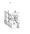
本発明は、端末計算機に製造しようとするロットの品種と工程を入力することで、作業できる設備の候補が出力される、手動の場合には、候補として出力された設備から設備のメンテナンス間隔や使用状況等の設備状態から設備を選択し、一つの設備を決めることで一つの製造条件を特定し、その条件を指示する。自動化された場合には、自動化を管理する計算機やシステムが設備群から一つの設備を選択し条件を一つに特定する。図1.に条件を特定する迄の概念を示した。条件を一つに特定することで、その条件を表示出力、または計算機出力により正確な作業ができる。
【0014】
作業終了時には、終了した作業ロットのナンバ、ウェハの枚数、作業時の状態としてプロセス上記録が必要なものについて端末計算機から入力したり、自動設備から製造条件の記録している計算機や更に上位のプロセス管理システムに、入力することで、後の製品製造来歴の検索や、不良解析の必要情報も提供できる。
【0015】
また、本発明は半導体と類似の製品である薄膜製品、液晶表示機の駆動用薄膜トランジスタ回路、配線板、磁気ディスクヘッドなどのプロセス技術を応用した製品にも適用できる。
【0016】
【実施例】
以下に本発明の実施例を図2から図8により説明する。
【0017】
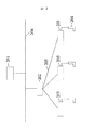
図2は本発明の半導体製造条件指示装置の構成図である。計算機201と端末計算機203から成る。計算機201と端末計算機203は通信容量の大きなネットワーク206で通信プロトコル変換器202と通信容量の小さなローカルネットワーク205を介して接続されている。また、端末計算機203にはバーコード入力用のバーコードリーダを接続している。製造条件の表示用の端末計算機203は半導体の製造設備の近傍に配置し、半導体製造ラインは塵埃の少ないクリーンルームであるため、小型でスペースの小さい計算機が好適である。これらの計算機では計算機201との通信をネットワーク206の大通信容量のネットワークをサポートしている機種が少なく、通信容量的には少ないローカルネットワーク205を介してプロトコル変換器202によりネットワーク206に接続している。
【0018】
図2の構成は製造ラインの作業が人手による場合である。作業する人は、製造しようとする製品ロットからその製品の型式と工程進行票から工程をキー、またはバーコードで入力する。
【0019】
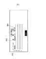
図3に入力の画面の1実施例を示す。この画面では製品のロットナンバを入力する欄301、製品型式の品種の入力欄302、工程の入力欄303がある。ロットナンバ、品種は基本的にコードであるが、工程名称は同一ベイ内や同一ライン内で全ての工程をユニークなコードとしておき、そのコードを入力する。入力後、送信のファンクションキー入力で検索が計算機201内部で処理される。
【0020】
また、これらの入力欄の行が複数あるのは、半導体の製造設備では製造ロットを1つの処理でなくバッチで処理する設備に対して対応するためである。
【0021】
上記品種、工程から使用する製造設備群を検索する。この設備群を規定した計算機201内部のコードは品種と工程のAND条件で1つに規定している。従って、複数の品種、工程を入力した際には、”送信”キーの入力により計算機201内部で各ロットの品種、工程の規定する内部コードが同一かをチェックし、もし異なっていれば、「製造条件が違う」旨のコメントを表示し作業者に注意を与え、条件を指示しない。
【0022】
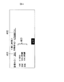
入力したロットの品種、工程が上記したチェックで異常がなければ、図4の画面になる。図4では上記の品種、工程の検索から設備群を表示したものである。設備の入力欄401には製造可能設備の一覧403から選択し、その設備のナンバを入力する。以上で1つの設備が特定できた。更にその作業を行った作業者のコードを入力欄402に入力し、”送信”キーを入力し、計算機201内部では設備から製造条件を規定しているコードに対応した製造条件ファイルを検索し出力する。その結果を図5に示す。
【0023】
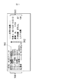
図5は条件が指示されて作業者がキー操作した後である。画面の向かって左側に製造条件を表示し作業者に指示している。指示条件の反転部501は作業者がその条件項目を確実に設備に設定したことを確認した項目を示している。これは作業者が確認し、リターンキーの操作で反転させている。
【0024】
条件項目の中には単純に指示できないものがある。製品の製作の回数により変化のある条件項目である。この変化条件項目502が変化する項目である。図5はスパッタの実施例であるが、スパッタの場合、成膜現象の累積によりターゲット材が減少し、プラズマ放電のポテンシャルが変化し成膜速度を変化させているので成膜時間を成膜速度に応じて替える必要がある。そのため、指示項目は範囲の指示になっている。そこで向かって右側の画面にその品種、工程の前回の作業の結果が参考値として表示している。
【0025】
このように変化する項目は、半導体の製造ではホトリソ工程の露光時間、エッチング時間などがある。
【0026】
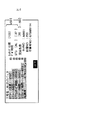
条件の確認が全項目終了すると図6のように画面の右側には作業の実績入力欄が表示され作業終了後、作業ロットの枚数の他、プロセスの実績値を入力し、先に述べた変化項目の参考値として使用する。
【0027】
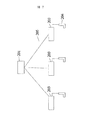
図7に本発明の別の実施例を示す。同図は半導体の製造条件を記憶する計算機201とその計算機と接続する端末計算機203からなり、前記計算機間はローカルなネットワークで接続されている。この構成とすることで他のシステムとの共存を考慮しなくも、本発明のみを製造ラインに導入することができる。端末計算機203の機能は上記した実施例の図3から図6までと同様の機能により製造条件の指示ができる。
【0028】
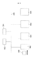
図8に本発明の別の実施例を示す。同図は図7と正反対の構成である。すなわち自動化した製造ラインに本発明を導入した実施例である。製造設備903、904、905から構成される製造ラインの一つのベイには、他のベイから搬送される製品の一時置場(ストッカ)901があり、搬送されてきた製品100は、ストッカ901に入れられる。ここでストッカ901は製品100のロットナンバ、品種、工程を自動で読み取り、または、ロットナンバからベイの管理計算機902に品種、工程を問い合わせ確認する。ここで入力入力された情報は管理計算機902に送信され、管理計算機902は、本発明の製造条件を記録している計算機201に問い合わせ、品種、工程から製造可能設備群の情報を取得する。管理計算機902は、設備群から自己の管理下にある製造設備903から905の状況に応じて設備を選択し、計算機201に設備の情報を送信し、製造条件の応答を貰う。この情報は管理計算機902が設備に条件を自動送信し作業を行う。作業の結果は設備から管理計算機902に送信されその情報は計算機201に管理計算機902から送信され、次の作業の条件の設定に使用する。
【0029】
【発明の効果】
本発明により、半導体ラインの製造条件の指示が正確、かつ迅速に行うことができ、ユーザニーズにあった半導体であるゲートアレイ等の生産には条件を間違えて不良になるようなケースを排除でき歩留りを向上できた。また、本発明はライン全体でなく部分的に導入適用できるので、ライン全体に適用する従来技術に比べて、10分の1程度の投資で、不良の低減効果をあげることができる。
【図面の簡単な説明】
【図1】本発明のデータ管理概念図である。
【図2】本発明の実施例構成図である。
【図3】本発明の入力画面を示す図である。
【図4】本発明の設備選択画面を示す図である。
【図5】本発明の条件の指示画面を示す図である。
【図6】本発明の実績入力画面を示す図である。
【図7】本発明のみの導入実施例を示す図である。
【図8】本発明の自動化導入実施例を示す図である。
【符号の説明】
201…計算機、
202…通信プロトコル変換機、
203…端末計算機、
205…ローカルネットワーク、
206…ネットワーク、
301…ロットナンバを入力する欄、
302…製品型式の品種の入力欄、
303…工程の入力欄、
401…設備の入力欄、
402…作業者のコードの入力欄、
501…指示条件の反転部、
502…変化条件項目。[0001]
[Industrial applications]
The present invention relates to the manufacture of semiconductors, and more particularly to an instruction method and an instruction device suitable for instructing production conditions during operation.
[0002]
[Prior art]
With the diversification of user needs, semiconductors tend not to produce a single memory in the past, but to produce a variety of products that meet the needs. Further, in response to the miniaturization of devices, the manufacturing conditions of various types of manufacturing equipment in the manufacturing process vary widely, and the control limit of the manufacturing conditions is limited to a very narrow range. For this reason, in order to quickly and accurately manufacture a wide variety of products, it is necessary to specify the conditions of the manufacturing lot for each manufacturing process and perform the operation. As a system for giving this instruction, for example, there is a “Wafer Processing Management System in VLSI Development” from pages 767 to 775 of “Transactions of the Institute of Electronics, Information and Communication Engineers, C Vol. J70-C No. 6” (June 1987). . In this system, the wafer processing specifications of the semiconductor are registered in advance on a 3.5-inch floppy disk before the manufacture, and the conditions are specified according to the semiconductor manufacturing process. is there. In this system, since the manufacturing process and manufacturing conditions of a manufacturing lot are recorded on a floppy disk, data can be produced by using a floppy disk and a computer capable of reading / writing the disk, thereby ensuring data reliability. . In addition, it is a distributed system that can be produced without a higher-level computer system.
[0003]
[Problems to be solved by the invention]
However, the production system has the following problems. First, floppy disks must be attached to product lots at all times, which is a major obstacle when introducing robots and automatic manufacturing equipment to promote automation of production lines. That is, it is necessary to automate the operation of making a computer read a floppy disk, in other words, the operation of inserting a disk into a disk drive. Even if this operation is automated, there is a problem that if there is an accident that the disk is dropped during transportation, the whole system stops.
[0004]
As a second problem, in the production system, since the processing specifications of the lot are registered in advance for each production lot, the same processing specification is changed for each production line input of the lot by changing the identifier of the lot even in the production of many kinds and small quantities. It needs to be created, that is, the lot number needs to be changed. At this time, there is a problem that a large number of defective products are manufactured when a registration error of the processing specifications occurs.
[0005]
The third problem, which is related to the first problem, requires a floppy disk, a read / write device and a computer. Therefore, a floppy disk, a read / write device and a computer are required for the entire production line, and when introducing a production condition indicating system, for example, resist removal (ashing) is often performed in a semiconductor production line. If the above conditions are not required and the operation is a manual operation, an inefficient situation may occur in which, for example, a floppy disk is sequentially mounted on a computer during the operation and the operation is performed while observing the conditions.
[0006]
An object of the present invention is that, even when a line incorporating robots or automatic manufacturing equipment or a line operated manually is used, when manufacturing a wide variety of products, it is possible to accurately and quickly instruct the conditions for manufacturing the product and to produce the product. When the present invention is introduced, the present invention for instructing the manufacturing conditions not only for the entire line but also for a part of the line can be introduced.
[0007]
[Means for Solving the Problems]
In order to achieve the above-mentioned object, as a minimum configuration capable of exhibiting the functions of the present invention, a computer in which manufacturing conditions are stored in advance and a terminal computer capable of displaying and outputting the contents of the conditions of the computer or outputting a computer signal are connected via a network. Consists of
[0008]
The reason for this configuration is that the semiconductor manufacturing process basically forms a film, or forms an impurity layer, photolithography, and repeats a large process of etching to form devices, resistors, capacitors, insulating layers, Wiring and the like are formed to manufacture a semiconductor integrated circuit (LSI). Therefore, one product is repeatedly subjected to manufacturing operations of different manufacturing processes in the same facility. For example, in the ion implantation step of forming an impurity layer, the ion implantation of the p-type well step and the ion implantation of the n-type well step in the element region are performed in the same equipment in the order of the steps, and the production operation is naturally performed under different conditions. Done. Therefore, manufacturing facilities having the same kind of functions are arranged in the same area. Such a line arrangement is called a bay system. For this reason, in the present invention, the conditions of the manufacturing facilities in the same area described above are stored in one computer, and the conditions can be instructed by a terminal computer to a person by display output, and automatic equipment can be instructed by a computer signal output.
[0009]
The range of the conditions stored in the computer is the product type and the process that can be performed by the manufacturing equipment in which the terminal computer having the configuration of the present invention indicates the manufacturing conditions. As the minimum unit, the same type of equipment group, that is, the bay is the minimum unit.
[0010]
The form of the manufacturing conditions to be recorded for instructing is such that there is a manufacturing process flow for each product type of the semiconductor, that is, for each product type. In such a case, conditions may be slightly different when manufacturing the same type of equipment, and the equipment is also stored. This is a data configuration of manufacturing conditions that can be determined as one manufacturing condition from these types, processes, and equipment.
[0011]
[Action]
The fact that the condition can be designated before the work by using the above-described condition form will be described below.
[0012]
Semiconductor products are usually stored in the form of wafers in a storage carrier called a cassette case, and move on a production line while being transported. At this time, the product in the line is in a wafer state, and the carrier is a medium indicating the product type (product type) of the wafer and the progress of the process, that is, a floppy disk in the case of the above-described conventional technology. Alternatively, a product type, a process progress form, and the like written on paper are attached to the carrier and manufactured while moving in the line.
[0013]
According to the present invention, by inputting the type and process of a lot to be manufactured to a terminal computer, candidates for equipment that can be operated are output. In the case of manual operation, equipment maintenance intervals and The equipment is selected from the equipment state such as the use status, and one equipment is determined to determine one manufacturing condition, and the condition is specified. In the case of automation, a computer or system that manages automation selects one facility from a facility group and specifies one condition. FIG. Shows the concept until the conditions are specified. By specifying one condition, the operation can be performed more accurately by displaying the condition on a display or outputting the result to a computer.
[0014]
At the end of the work, the number of the completed work lot, the number of wafers, and the state of the work that need to be recorded in the process are input from the terminal computer, or the computer that records the manufacturing conditions from the automatic equipment or a higher-level computer. By inputting the information to the process management system, it is possible to search for the history of product manufacturing later and provide necessary information for failure analysis.
[0015]
In addition, the present invention can be applied to thin film products similar to semiconductors, thin film transistor circuits for driving liquid crystal displays, wiring boards, magnetic disk heads, and other products to which process technology is applied.
[0016]
【Example】
An embodiment of the present invention will be described below with reference to FIGS.
[0017]
FIG. 2 is a configuration diagram of the semiconductor manufacturing condition indicating apparatus of the present invention. It comprises a
[0018]
The configuration in FIG. 2 is a case where the operation of the production line is performed manually. A worker inputs a process from a product lot to be manufactured by a key or a bar code based on a model of the product and a process progress form.
[0019]
FIG. 3 shows an embodiment of the input screen. On this screen, there are a
[0020]
The reason why there are a plurality of rows in these input fields is to accommodate equipment that processes batches in a semiconductor manufacturing facility instead of one process.
[0021]
Search the manufacturing equipment group to be used from the above product types and processes. The code in the
[0022]
If there is no abnormality in the entered lot type and process in the above check, the screen shown in FIG. 4 is displayed. In FIG. 4, the equipment group is displayed from the search for the type and process. In the
[0023]
FIG. 5 shows a state after the condition is specified and the operator performs a key operation. The manufacturing conditions are displayed on the left side of the screen to instruct the operator. The instruction
[0024]
Some condition items cannot be simply specified. This is a condition item that changes depending on the number of times the product is manufactured. The
[0025]
Items that change in this way include the exposure time and the etching time of the photolithography step in the manufacture of semiconductors.
[0026]
When all items have been checked, a work result input field is displayed on the right side of the screen as shown in FIG. 6. After the work is completed, the actual work value is input in addition to the number of work lots. Use as a reference value for the item.
[0027]
FIG. 7 shows another embodiment of the present invention. The figure includes a
[0028]
FIG. 8 shows another embodiment of the present invention. This figure is the exact opposite configuration from FIG. That is, this is an embodiment in which the present invention is introduced into an automated manufacturing line. One bay of a manufacturing line including
[0029]
【The invention's effect】
ADVANTAGE OF THE INVENTION According to this invention, the instruction | indication of the manufacturing conditions of a semiconductor line can be performed correctly and promptly, and the case where the conditions are mistaken in the production of the gate array etc. which is the semiconductor which met the user's needs can be eliminated. The yield was improved. Further, since the present invention can be applied to a part of the line instead of the entire line, the effect of reducing defects can be improved with an investment of about one tenth as compared with the conventional technology applied to the entire line.
[Brief description of the drawings]
FIG. 1 is a conceptual diagram of data management according to the present invention.
FIG. 2 is a configuration diagram of an embodiment of the present invention.
FIG. 3 is a diagram showing an input screen of the present invention.
FIG. 4 is a diagram showing a facility selection screen of the present invention.
FIG. 5 is a diagram showing a condition instruction screen of the present invention.
FIG. 6 is a diagram showing a result input screen of the present invention.
FIG. 7 is a diagram showing an introduction example of only the present invention.
FIG. 8 is a diagram showing an example of the automatic introduction of the present invention.
[Explanation of symbols]
201 ... Calculator,
202: communication protocol converter
203: terminal computer,
205 ... local network,
206 ... network,
301: A field for inputting a lot number
302: Input field for product type type,
303 ... input field of the process,
401 ... input field for equipment,
402: an input field for an operator code;
501: Inversion part of instruction condition,
502: Change condition item.
Claims (1)
前記管理計算機は、
ロットの品種と工程と製造設備とから製造条件を特定できるデータベースを備え、
ロットの品種と工程の入力があった場合に、それらの入力をキーにデータベースから該品種の該工程で作業できる製造設備の候補を検索し、検索した結果である製造設備の候補から該工程に対する製造設備が選択された場合に、選択された製造設備の製造条件を当該製造設備に対して製造条件を指示する端末計算機に表示させる計算機であることを特徴とする半導体製造条件指示装置。 A semiconductor manufacturing condition indicating apparatus including a management computer connected via a network to a terminal computer for indicating manufacturing conditions to a manufacturing facility ,
The management computer,
Equipped with a database that can specify manufacturing conditions from lot types, processes, and manufacturing equipment,
When there is an input of a lot type and a process, the input is used as a key to search a database for a candidate of manufacturing equipment that can work in the process of the type, and from the candidate of the manufacturing equipment obtained as a result of the search, to the process. If the manufacturing facility is selected, the semiconductor manufacturing conditions indicating device, characterized in that the computer for displaying the production conditions of the selected manufacturing equipment to a terminal computer for instructing the manufacturing conditions with respect to the manufacturing equipment.
Priority Applications (1)
| Application Number | Priority Date | Filing Date | Title |
|---|---|---|---|
| JP5370893A JP3575813B2 (en) | 1993-03-15 | 1993-03-15 | Semiconductor manufacturing condition indicating device |
Applications Claiming Priority (1)
| Application Number | Priority Date | Filing Date | Title |
|---|---|---|---|
| JP5370893A JP3575813B2 (en) | 1993-03-15 | 1993-03-15 | Semiconductor manufacturing condition indicating device |
Publications (2)
| Publication Number | Publication Date |
|---|---|
| JPH06267805A JPH06267805A (en) | 1994-09-22 |
| JP3575813B2 true JP3575813B2 (en) | 2004-10-13 |
Family
ID=12950335
Family Applications (1)
| Application Number | Title | Priority Date | Filing Date |
|---|---|---|---|
| JP5370893A Expired - Fee Related JP3575813B2 (en) | 1993-03-15 | 1993-03-15 | Semiconductor manufacturing condition indicating device |
Country Status (1)
| Country | Link |
|---|---|
| JP (1) | JP3575813B2 (en) |
-
1993
- 1993-03-15 JP JP5370893A patent/JP3575813B2/en not_active Expired - Fee Related
Also Published As
| Publication number | Publication date |
|---|---|
| JPH06267805A (en) | 1994-09-22 |
Similar Documents
| Publication | Publication Date | Title |
|---|---|---|
| CN101978389B (en) | Vao productivity suite | |
| Cunningham et al. | Semiconductor yield improvement: results and best practices | |
| US7162326B1 (en) | Mask identification database server | |
| CN1744116B (en) | Method and system for semiconductor production automation | |
| WO2007078755A1 (en) | Integrated configuration, flow and execution system for semiconductor device experimental flows and production flows | |
| Hughes et al. | The future of automation for high-volume wafer fabrication and ASIC manufacturing | |
| US7016753B2 (en) | Management system for production line and management method for production line | |
| US6618639B2 (en) | System, process, apparatus and program for controlling special lot carrying in semiconductor carrying facility | |
| JPH08335539A (en) | Production control device and production control method | |
| JP3575813B2 (en) | Semiconductor manufacturing condition indicating device | |
| Lin et al. | The performance of the number of vehicles in a dynamic connecting transport AMHS | |
| JP2792800B2 (en) | Manufacturing process management system | |
| JP2001044091A (en) | Semiconductor factory automation system and automation method | |
| JP2004241697A (en) | Semiconductor wafer production management device | |
| JP3301228B2 (en) | Process control method for articles in the manufacturing process | |
| JP4429578B2 (en) | Production method of composite products | |
| JP2003228412A (en) | Managing system of production line | |
| JP3049871B2 (en) | Reference wafer single wafer management system | |
| JP2666714B2 (en) | Production equipment control data management system | |
| US20010039463A1 (en) | Device and method for supporting system development and computer-readable medium | |
| JP2743908B2 (en) | Semiconductor device manufacturing equipment | |
| JPH04275667A (en) | Mold management method, mold, mold usage equipment, and mold management system | |
| JP2523638B2 (en) | Semiconductor equipment operation data collection method | |
| JPH1153439A (en) | Automatic recipe determination method for manufacturing equipment | |
| JP2005208889A (en) | Control apparatus and processing system |
Legal Events
| Date | Code | Title | Description |
|---|---|---|---|
| RD02 | Notification of acceptance of power of attorney |
Free format text: JAPANESE INTERMEDIATE CODE: A7422 Effective date: 20040309 |
|
| A131 | Notification of reasons for refusal |
Free format text: JAPANESE INTERMEDIATE CODE: A131 Effective date: 20040330 |
|
| A521 | Written amendment |
Free format text: JAPANESE INTERMEDIATE CODE: A523 Effective date: 20040531 |
|
| TRDD | Decision of grant or rejection written | ||
| A01 | Written decision to grant a patent or to grant a registration (utility model) |
Free format text: JAPANESE INTERMEDIATE CODE: A01 Effective date: 20040629 |
|
| A61 | First payment of annual fees (during grant procedure) |
Free format text: JAPANESE INTERMEDIATE CODE: A61 Effective date: 20040706 |
|
| R150 | Certificate of patent or registration of utility model |
Free format text: JAPANESE INTERMEDIATE CODE: R150 |
|
| FPAY | Renewal fee payment (event date is renewal date of database) |
Free format text: PAYMENT UNTIL: 20080716 Year of fee payment: 4 |
|
| FPAY | Renewal fee payment (event date is renewal date of database) |
Free format text: PAYMENT UNTIL: 20080716 Year of fee payment: 4 |
|
| FPAY | Renewal fee payment (event date is renewal date of database) |
Free format text: PAYMENT UNTIL: 20090716 Year of fee payment: 5 |
|
| FPAY | Renewal fee payment (event date is renewal date of database) |
Free format text: PAYMENT UNTIL: 20100716 Year of fee payment: 6 |
|
| FPAY | Renewal fee payment (event date is renewal date of database) |
Free format text: PAYMENT UNTIL: 20110716 Year of fee payment: 7 |
|
| FPAY | Renewal fee payment (event date is renewal date of database) |
Free format text: PAYMENT UNTIL: 20110716 Year of fee payment: 7 |
|
| S111 | Request for change of ownership or part of ownership |
Free format text: JAPANESE INTERMEDIATE CODE: R313111 |
|
| FPAY | Renewal fee payment (event date is renewal date of database) |
Free format text: PAYMENT UNTIL: 20110716 Year of fee payment: 7 |
|
| R350 | Written notification of registration of transfer |
Free format text: JAPANESE INTERMEDIATE CODE: R350 |
|
| FPAY | Renewal fee payment (event date is renewal date of database) |
Free format text: PAYMENT UNTIL: 20120716 Year of fee payment: 8 |
|
| LAPS | Cancellation because of no payment of annual fees |