JP3582964B2 - Driving device for plasma display panel - Google Patents
Driving device for plasma display panel Download PDFInfo
- Publication number
- JP3582964B2 JP3582964B2 JP23413897A JP23413897A JP3582964B2 JP 3582964 B2 JP3582964 B2 JP 3582964B2 JP 23413897 A JP23413897 A JP 23413897A JP 23413897 A JP23413897 A JP 23413897A JP 3582964 B2 JP3582964 B2 JP 3582964B2
- Authority
- JP
- Japan
- Prior art keywords
- mos transistor
- pulse
- state
- line
- row electrode
- Prior art date
- Legal status (The legal status is an assumption and is not a legal conclusion. Google has not performed a legal analysis and makes no representation as to the accuracy of the status listed.)
- Expired - Fee Related
Links
- 238000010586 diagram Methods 0.000 description 20
- 239000003990 capacitor Substances 0.000 description 17
- 230000004044 response Effects 0.000 description 6
- 238000000034 method Methods 0.000 description 5
- 230000015556 catabolic process Effects 0.000 description 4
- 230000037452 priming Effects 0.000 description 4
- 230000007423 decrease Effects 0.000 description 3
- 230000003071 parasitic effect Effects 0.000 description 3
- 239000002245 particle Substances 0.000 description 3
- 229910044991 metal oxide Inorganic materials 0.000 description 2
- 150000004706 metal oxides Chemical class 0.000 description 2
- 239000004065 semiconductor Substances 0.000 description 2
- 238000001514 detection method Methods 0.000 description 1
Images




Classifications
-
- G—PHYSICS
- G09—EDUCATION; CRYPTOGRAPHY; DISPLAY; ADVERTISING; SEALS
- G09G—ARRANGEMENTS OR CIRCUITS FOR CONTROL OF INDICATING DEVICES USING STATIC MEANS TO PRESENT VARIABLE INFORMATION
- G09G3/00—Control arrangements or circuits, of interest only in connection with visual indicators other than cathode-ray tubes
- G09G3/20—Control arrangements or circuits, of interest only in connection with visual indicators other than cathode-ray tubes for presentation of an assembly of a number of characters, e.g. a page, by composing the assembly by combination of individual elements arranged in a matrix no fixed position being assigned to or needed to be assigned to the individual characters or partial characters
- G09G3/22—Control arrangements or circuits, of interest only in connection with visual indicators other than cathode-ray tubes for presentation of an assembly of a number of characters, e.g. a page, by composing the assembly by combination of individual elements arranged in a matrix no fixed position being assigned to or needed to be assigned to the individual characters or partial characters using controlled light sources
- G09G3/28—Control arrangements or circuits, of interest only in connection with visual indicators other than cathode-ray tubes for presentation of an assembly of a number of characters, e.g. a page, by composing the assembly by combination of individual elements arranged in a matrix no fixed position being assigned to or needed to be assigned to the individual characters or partial characters using controlled light sources using luminous gas-discharge panels, e.g. plasma panels
- G09G3/288—Control arrangements or circuits, of interest only in connection with visual indicators other than cathode-ray tubes for presentation of an assembly of a number of characters, e.g. a page, by composing the assembly by combination of individual elements arranged in a matrix no fixed position being assigned to or needed to be assigned to the individual characters or partial characters using controlled light sources using luminous gas-discharge panels, e.g. plasma panels using AC panels
- G09G3/296—Driving circuits for producing the waveforms applied to the driving electrodes
- G09G3/2965—Driving circuits for producing the waveforms applied to the driving electrodes using inductors for energy recovery
-
- G—PHYSICS
- G09—EDUCATION; CRYPTOGRAPHY; DISPLAY; ADVERTISING; SEALS
- G09G—ARRANGEMENTS OR CIRCUITS FOR CONTROL OF INDICATING DEVICES USING STATIC MEANS TO PRESENT VARIABLE INFORMATION
- G09G2330/00—Aspects of power supply; Aspects of display protection and defect management
- G09G2330/02—Details of power systems and of start or stop of display operation
Landscapes
- Engineering & Computer Science (AREA)
- Power Engineering (AREA)
- Physics & Mathematics (AREA)
- Plasma & Fusion (AREA)
- Computer Hardware Design (AREA)
- General Physics & Mathematics (AREA)
- Theoretical Computer Science (AREA)
- Control Of Indicators Other Than Cathode Ray Tubes (AREA)
- Control Of Gas Discharge Display Tubes (AREA)
- Transforming Electric Information Into Light Information (AREA)
Description
【0001】
【発明の属する技術分野】
本発明はプラズマディスプレイパネルの駆動装置に関する。
【0002】
【従来の技術】
平面表示装置として、AC(交流放電)型のプラズマディスプレイパネル(以下、PDPと称する)が知られている。
図1は、かかるAC型のPDPを駆動する駆動装置を含んだプラズマディスプレイ装置の概略構成を示す図である。
【0003】
図1において、PDP10には、X及びYの1対にて1画面の各行(第1行〜第n行)に対応した行電極対を為す行電極Y1〜Yn及び行電極X1〜Xnが形成されている。更に、これら行電極対に直交し、かつ図示せぬ誘電体層及び放電空間を挟んで、1画面の各列(第1列〜第m列)に対応した列電極を為す列電極D1〜Dmが形成されている。この際、1対の行電極対(X、Y)と1つの列電極Dとの交差部に1つの放電セルが形成される。駆動装置1は、供給された映像信号を1画素毎のNビットの画素データに変換し、これをPDP10における1行分毎にm個の画素データパルスに変換してPDP10の列電極D1〜Dm各々に印加する。更に、駆動装置1は、図2に示されるが如きタイミングにて、リセットパルスRPX、リセットパルスRPY、プライミングパルスPP、走査パルスSP、維持パルスIPX、維持パルスIPY、及び消去パルスEP各々を含んだ行電極駆動信号を生成し、これを上記PDP10の行電極対(Y1〜Yn、X1〜Xn)に印加する。
【0004】
図2において、駆動装置1は、先ず、正電圧のリセットパルスRPxを発生してこれを全ての行電極X1〜Xnに印加すると同時に、負電圧のリセットパルスRPyを発生してこれを行電極Y1〜Yn の各々に印加する(一斉リセット行程)。かかるリセットパルスの印加によりPDP10の全ての放電セルが放電励起して荷電粒子が発生し、この放電終息後、全放電セルの誘電体層には一様に所定量の壁電荷が形成される。
【0005】
次に、駆動装置1は、各行毎の画素データに対応した正電圧の画素データパルスDP1〜DPmを発生し、これらを1行分毎に順次、列電極D1〜Dmに印加して行く。更に、駆動装置1は、上記画素データパルスDP1〜DPmを列電極D1〜Dmに印加するタイミングと同一タイミングにて、負電圧でありかつ比較的パルス幅の小なる走査パルスSPを発生し、これを図2に示されるように、行電極Y1からYnへと順次印加して行く。この際、走査パルスSPが印加された行電極に存在する放電セルの内で、高電圧の画素データパルスが印加された放電セルでは放電が生じてその壁電荷の大半が失われる。一方、画素データパルスが印加されなかった放電セルでは放電が生じないので、上記壁電荷が残留したままとなる。すなわち、列電極に印加された画素データパルスに応じて、各放電セル内に壁電荷が残留するか否かが決定するのである。これは、走査パルスSPの印加に応じて、各放電セルに対して画素データの書き込みが為されたということなのである。尚、駆動装置1は、かかる負電圧の走査パルスSPを各行電極Yに印加する直前に、図2に示されるが如き正電圧のプライミングパルスPPを行電極Y1〜Ynに印加する(画素データ書込行程)。
【0006】
かかるプライミングパルスPPの印加により、上記一斉リセット動作にて得られ、時間経過と共に減少してしまった上記荷電粒子が、PDP10の放電空間内に再形成される。よって、かかる荷電粒子が存在する内に、上記走査パルスSPの印加による画素データの書き込みが為されることになる。
次に、駆動装置1は、正電圧の維持パルスIPYを連続して行電極Y1〜Yn 各々に印加すると共に、かかる維持パルスIPYの印加タイミングとは、ずれたタイミングにて正電圧の維持パルスIPXを連続して行電極X1〜Xn各々に印加する(維持放電行程)。
【0007】
かかる維持パルスIPX及びIPYが交互に印加されている期間に亘り、上記壁電荷が残留したままとなっている放電セルが放電発光を繰り返しその発光状態を維持する。
次に、駆動装置1は、負電圧の消去パルスEPを発生してこれを行電極Y1〜Yn各々に一斉に印加して、各放電セル内に残留している壁電荷を消去する(壁電荷消去行程)。
【0008】
図3は、上記各種駆動パルスの内で、上記リセットパルスRPY及び維持パルスIPYを発生するパルス駆動回路の構成を示す図である。
図3において、維持パルス発生回路102におけるpチャネル型のMOS(Metal Oxide Semiconductor)トランジスタQ1は、そのゲート端に供給されたゲート信号GT1の論理レベルが”1”である場合にはオフ状態となる。又、かかるMOSトランジスタQ1は、ゲート信号GT1の論理レベルが”0”である場合にはオン状態となって上記直流電源B1の正側端子電位をライン2上に印加する。尚、この直流電源B1の負側端子は接地されている。更に、かかる維持パルス発生回路102には、その一端が接地されているコンデンサC1が設けられている。nチャネル型のMOSトランジスタQ2は、そのゲート端に供給されたゲート信号GT2の論理レベルが”0”である場合にはオフ状態となる一方、かかるゲート信号GT2の論理レベルが”1”である場合にはオン状態となって上記ライン2上の電位をダイオードD1及びコイルL1を介して上記コンデンサC1の他端に印加する。nチャネル型のMOSトランジスタQ3は、そのゲート端に供給されたゲート信号GT3の論理レベルが”0”である場合にはオフ状態となる一方、かかるゲート信号GT3の論理レベルが”1”である場合にはオン状態となって上記コンデンサC1の他端に生じた電位をダイオードD2及びコイルL2を介して上記ライン2上に印加する。pチャネル型のMOSトランジスタQ4は、そのゲート端に供給されたゲート信号GT4の論理レベルが”1”である場合にはオフ状態となる一方、かかるゲート信号GT4の論理レベルが”0”である場合にはオン状態となって上記ライン2上の電位をダイオードD3を介して接地電位に引き込む。
【0009】
リセットパルス発生回路103におけるnチャネル型のMOSトランジスタQ5は、そのゲート端に供給されたゲート信号GT5の論理レベルが”0”である場合にはオフ状態となる。又、かかるMOSトランジスタQ5は、ゲート信号GT5の論理レベルが”1”である場合にはオン状態となって直流電源B2の負側端子電位を抵抗R1を介してライン2上に印加する。尚、この直流電源B2の正側端子は接地されている。nチャネル型のMOSトランジスタQ6は、そのゲート端に供給されたゲート信号GT6の論理レベルが”0”である場合にはオフ状態となる一方、かかるゲート信号GT6の論理レベルが”1”である場合にはオン状態となって上記ライン2上の電位をダイオードD4を介して接地電位に引き込む。
【0010】
尚、上記ダイオードD1〜D4は逆流防止の為に設けられたものである。
図4は、上記図2に示されるが如きリセットパルスRPy及び維持パルスIPy各々を発生させる際の上記ゲート信号GT1〜GT6各々の供給タイミングを示す図である。
図4に示されるように、先ず、論理レベル”1”のゲート信号GT5に応じてMOSトランジスタQ5がオン状態となる。これにより、直流電源B2の負側端子に発生した負の電位がライン2上に印加されて図4に示されるが如き負電圧を有するリセットパルスRPyが発生する。
【0011】
次に、図4に示されるように、ゲート信号GT3の論理レベルが”0”〜”1”〜”0”、ゲート信号GT3の論理レベルが”1”〜”0”〜”1”、更にゲート信号GT2の論理レベルが”0”〜”1”〜”0”へと順次切り替わることにより、図4に示される正電圧の維持パルスIPyが発生する。つまり、先ず、論理レベル”1”のゲート信号GT3に応じて、MOSトランジスタQ3がオン状態となり、コンデンサC1に蓄積されていた電荷に応じた電流がMOSトランジスタQ3、ダイオードD2、及びコイルL2を介してライン2上に流れ込む。これにより、ライン2上の行電極駆動信号のレベルは、図4に示されるように徐々に上昇して行く。次に、論理レベル”1”のゲート信号GT1に応じて、MOSトランジスタQ1がオン状態となる。これにより、直流電源B1の正側端子の正電位がライン2上に印加されて、図4に示されるが如き正電圧を有する維持パルスIPyが発生する。次に、論理レベル”1”のゲート信号GT2に応じてMOSトランジスタQ2がオン状態となる。これにより、PDP10に帯電されていた電荷に応じた電流がMOSトランジスタQ2、ダイオードD1、及びコイルL1を介してコンデンサC1に流れ込む。かかるコンデンサC1の充電動作により、上記維持パルスIPyのレベルは、図4に示されるように徐々に下降して行く。
【0012】
以上の如く、リセットパルス発生回路102及び維持パルス発生回路103各々は、互いに極性の異なる駆動パルス(リセットパルスRPy、維持パルスIPy)を発生し、これらを異なるタイミングで共通のライン2上に印加する構成となっている。
ここで、かかる図3に示される構成では、直流電源B1の正側端子と直流電源B2の負側端子との間に、MOSトランジスタQ1及びQ5が直列に接続される形となる。更に、かかる直流電源B1の正側端子と略同一の電位を発生するコンデンサC1と直流電源B2の負側端子との間には、MOSトランジスタQ2(Q3)及びQ5が直列に接続される形となる。
【0013】
従って、かかる図3に示されるMOSトランジスタQ1〜Q3、及びQ4としては、直流電源B1の正側端子電位と直流電源B2の負側端子電位との電位差に耐え得る高耐圧なトランジスタを用いなければならないという問題があった。
【0014】
【発明が解決しようとする課題】
本発明は、上記問題を解決するために為されたものであり、比較的耐圧の低いトランジスタにて互いに極性の異なる複数の駆動パルスをPDPの同一行電極上に印加し得るプラズマディスプレイパネルの駆動装置を提供することを目的とする。
【0015】
【課題を解決するための手段】
本発明の第1の特徴によるプラズマディスプレイパネルの駆動方法は、プラズマディスプレイパネルの垂直方向に配列された複数の列電極に画素データに対応した画素データパルスを印加する列電極駆動手段と、前記列電極に交差する水平方向に配列された複数の行電極に所定極性の第1パルス及び前記所定極性とは異なる極性の第2パルスを夫々印加する行電極駆動手段とを備えたプラズマディスプレイパネルの駆動装置であって、前記行電極駆動手段は、オン状態時に前記第1パルスを発生してこれを駆動ラインに印加するp型の第1MOSトランジスタと、オン状態時に前記第2パルスを発生してこれを前記行電極に印加するn型の第2MOSトランジスタと、オン状態時に前記駆動ラインと前記行電極とを接続するp型の第3MOSトランジスタと、前記第1MOSトランジスタをオン状態に設定する場合には前記第3MOSトランジスタをオン状態に設定すると共に前記第2MOSトランジスタをオフ状態に設定する一方、前記第2MOSトランジスタをオン状態に設定する場合には前記第3MOSトランジスタをオフ状態に設定する制御回路と、を有することを特徴とする。
【0016】
又、本発明の第2の特徴によるプラズマディスプレイパネルの駆動方法は、プラズマディスプレイパネルの垂直方向に配列された複数の列電極に画素データに対応した画素データパルスを印加する列電極駆動手段と、前記列電極に交差する水平方向に配列された複数の行電極に所定極性の第1パルス及び前記所定極性とは異なる極性の第2パルスを夫々印加する行電極駆動手段とを備えたプラズマディスプレイパネルの駆動装置であって、前記行電極駆動手段は、オン状態時に前記第1パルスを発生してこれを第1ラインに印加するp型の第1MOSトランジスタと、オン状態時に前記第1ライン及び前記行電極間を接続するp型の第2MOSトランジスタと、オン状態時に前記第2パルスを発生してこれを第2ラインに印加するn型の第3MOSトランジスタと、オン状態時に前記第2ライン及び前記行電極間を接続するn型の第4MOSトランジスタと、前記第1MOSトランジスタをオン状態に設定する場合には前記第2MOSトランジスタをオン状態に設定すると共に前記第4MOSトランジスタをオフ状態に設定する一方、前記第3MOSトランジスタをオン状態に設定する場合には前記第2MOSトランジスタをオフ状態に設定すると共に前記第4MOSトランジスタをオン状態に設定する制御回路と、を有することを特徴とする。
【0017】
【発明の実施の形態】
以下、本発明の実施例を図を参照しつつ説明する。
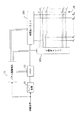
図5は、本発明による駆動装置を含んだプラズマディスプレイ装置の全体構成を示す図である。
かかる図5において、A/D変換器11は、供給されてきたアナログの映像信号をサンプリングして1画素毎のNビットの画素データに変換しこれをメモリ13に供給する。パネル駆動制御回路12は、かかる映像信号中に含まれる水平同期信号及び垂直同期信号を検出し、この検出タイミングに基づいて以下に説明するが如き各種信号を生成し、これらをメモリ13、行電極ドライバ100、及び列電極ドライバ200の各々に供給する。
【0018】
メモリ13は、パネル駆動制御回路12から供給されてくる書込信号に応じて上記画素データを順次書き込む。更に、メモリ13は、上記パネル駆動制御回路12から供給されてくる読出信号に応じて、上述の如く書き込まれた画素データをPDP(プラズマディスプレイパネル)20の1行分毎に読み出し、これを列電極ドライバ200に供給する。
【0019】
PDP20には、X及びYの1対にて1画面の各行(第1行〜第n行)に対応した行電極対を為す行電極Y1〜Yn及び行電極X1〜Xnが形成されている。更に、これら行電極対に直交し、かつ図示せぬ誘電体層及び放電空間を挟んで、1画面の各列(第1列〜第m列)に対応した列電極を為す列電極D1〜Dmが形成されている。この際、1対の行電極対(X、Y)と1つの列電極Dとの交差部に1つの放電セルが形成される。
【0020】
列電極ドライバ200は、上記メモリ13から供給されてくる1行分の画素データ各々に対応した画素データパルスDP1〜mを発生し、これらを上記パネル駆動制御回路12から供給される画素データパルス印加タイミング信号に応じて、図6に示されるように上記PDP20の列電極D1〜Dm各々に印加する。
行電極ドライバ100は、上記パネル駆動制御回路12から供給されてくる各種タイミング信号に応じて、上記図6に示されるが如きリセットパルスRPX及び維持パルスIPXを含んだ行電極X駆動信号を生成し、これを上記PDP20の行電極X1〜Xn各々に同時に印加する。又、行電極ドライバ100は、上記パネル駆動制御回路12から供給されてくる各種タイミング信号に応じて、上記図6に示されるが如き負電圧のリセットパルスRPY、正電圧のプライミングパルスPP、負電圧の走査パルスSP、正電圧の維持パルスIPY及び負電圧の消去パルスEP各々を含んだ行電極Y駆動信号を生成し、これを上記PDP20の行電極Y1〜Yn各々に印加する。
【0021】
図7は、上記各種駆動パルスの内からリセットパルスRPY及び維持パルスIPY各々を発生すべく為された本発明の駆動装置に基づくパルス駆動回路の構成を示す図である。尚、この図7に示される構成は、上記行電極ドライバ100内に設けられているものである。
図7において、維持パルス発生回路120におけるpチャネル型のMOS(Metal Oxide Semiconductor)トランジスタQ1は、上記パネル駆動制御回路12から供給されたゲート信号GT1の論理レベルが”1”である場合にはオフ状態となる。一方、このゲート信号GT1の論理レベルが”0”である場合には、上記MOSトランジスタQ1はオン状態となって上記直流電源B1の正側端子電位をライン200上に印加する。尚、この直流電源B1の負側端子は接地されている。更に、かかる維持パルス発生回路120には、その一端が接地されているコンデンサC1が設けられている。nチャネル型のMOSトランジスタQ2は、上記パネル駆動制御回路12から供給されたゲート信号GT2の論理レベルが”0”である場合にはオフ状態となる。一方、かかるゲート信号GT2の論理レベルが”1”である場合には、MOSトランジスタQ2はオン状態となって上記ライン200上の電位をダイオードD1及びコイルL1を介して上記コンデンサC1の他端に印加してこれを充電する。nチャネル型のMOSトランジスタQ3は、上記パネル駆動制御回路12から供給されたゲート信号GT3の論理レベルが”0”である場合にはオフ状態となる。一方、かかるゲート信号GT3の論理レベルが”1”である場合には、MOSトランジスタQ3はオン状態となって上記コンデンサC1の他端から放電された電位をダイオードD2及びコイルL2を介して上記ライン200上に印加する。pチャネル型のMOSトランジスタQ4は、上記パネル駆動制御回路12から供給されたゲート信号GT4の論理レベルが”1”である場合にはオフ状態となる一方、かかるゲート信号GT4の論理レベルが”0”である場合にはオン状態となって上記ライン200上の電位を接地電位に引き込む。
【0022】
リセットパルス発生回路130におけるnチャネル型のMOSトランジスタQ5は、上記パネル駆動制御回路12から供給されたゲート信号GT5の論理レベルが”0”である場合にはオフ状態となる。又、かかるMOSトランジスタQ5は、ゲート信号GT5の論理レベルが”1”である場合にはオン状態となって直流電源B2の負側端子の電位を抵抗R1を介してライン300上に印加する。尚、この直流電源B2の正側端子は接地されている。
【0023】
スイッチング素子としてのpチャネル型のMOSトランジスタQ7は、上記パネル駆動制御回路12から供給されたゲート信号GT7の論理レベルが”0”である場合にはオン状態となって上記ライン200及びライン300間の接続を行う。この際、かかるライン200上に発生した行電極駆動信号は上記ライン300を介してPDP20の各行電極Y1〜Ynに印加される。一方、かかるゲート信号GT7の論理レベルが”1”である場合には、MOSトランジスタQ7はオフ状態となり、上記ライン200及びライン300間の接続を遮断する。この際、上記ライン300上に発生した行電極駆動信号のみがPDP20の各行電極Y1〜Ynに印加される。
【0024】
図8は、上記ゲート信号GT1〜GT5及びGT7各々のタイミング、及びこれらゲート信号GTに応じてライン300上に生成される行電極駆動信号の波形を示す図である。
図8は、上記図6に示されるが如きリセットパルスRPy及び維持パルスIPy各々を発生させる際の上記ゲート信号GT1〜GT5及びGT7各々の供給タイミングを示す図である。
【0025】
図8に示されるように、先ず、論理レベル”1”のゲート信号GT5に応じて図7に示されるMOSトランジスタQ5がオン状態となる。これにより、直流電源B2の負側端子に発生した負の電位が抵抗R1を介してライン300上に印加されて、図8に示されるが如き負電圧のリセットパルスRPyがPDP20の行電極Yに印加される。この際、かかる抵抗R1の作用により、上記リセットパルスRPyのフロントエッジ部の波形はなだらかになる。又、この間、図7に示されるMOSトランジスタQ7には、論理レベル”1”のゲート信号GT7が供給されているので、MOSトランジスタQ7はオフ状態にある。よって、少なくとも上記リセットパルスRPyが発生している期間中は、ライン200及びライン300間は遮断された状態にある。
【0026】
次に、図8に示されるように、ゲート信号GT3の論理レベルが”0”〜”1”〜”0”、ゲート信号GT3の論理レベルが”1”〜”0”〜”1”、更にゲート信号GT2の論理レベルが”0”〜”1”〜”0”へと順次切り替わることにより、図8に示されるが如き正電圧の維持パルスIPyが発生する。つまり、先ず、論理レベル”1”のゲート信号GT3に応じて、MOSトランジスタQ3がオン状態となり、コンデンサC1に蓄積されていた電荷に応じた電流がMOSトランジスタQ3、ダイオードD2、及びコイルL2を介してライン200上に流れ込む。この際、図8に示されるようにMOSトランジスタQ7には論理レベル”0”のゲート信号GT7が供給されているので、MOSトランジスタQ7はオン状態にあり、ライン200及び300間が接続される。これにより、ライン300上の行電極駆動信号のレベルは、図8に示されるように徐々に上昇して行く。次に、論理レベル”1”のゲート信号GT1に応じて、MOSトランジスタQ1がオン状態となる。これにより、直流電源B1の正側端子の正電位がライン200及びMOSトランジスタQ7を介してライン300上に印加されて、図8に示されるが如き正電圧を有する維持パルスIPyが発生する。次に、論理レベル”1”のゲート信号GT2に応じてMOSトランジスタQ2がオン状態となる。これにより、PDP20に帯電されていた電荷に応じた電流がMOSトランジスタQ2、ダイオードD1、及びコイルL1を介してコンデンサC1に流れ込む。かかるコンデンサC1の充電動作により、上記維持パルスIPyのレベルは、図8に示されるように徐々に下降して行く。
【0027】
以上の如く、図7に示されるパルス駆動回路においては、少なくとも維持パルスを行電極に印加する期間中はオン状態となるMOSトランジスタQ7を維持パルス発生回路120及びリセットパルス発生回路130間に設ける構成としたのである。
かかる構成によれば、直流電源B1の正側端子と直流電源B2の負側端子との間、更に、直流電源B1の正側端子と略同一の電位を発生するコンデンサC1と直流電源B2の負側端子との間各々に直列に接続されるMOSトランジスタの数が、MOSトランジスタQ7の分だけ1段増えることになる。
【0028】
よって、図3に示されるが如き従来の構成に比してMOSトランジスタ1段あたりの耐圧を低くすることが出来るのである。
又、図7に示されるMOSトランジスタQ7は等価的には、図9に示されるように、ゲート信号GT7に応じてライン200及びライン300間の接続/遮断を為すスイッチSW7、及びライン300からライン200に向けて順方向に形成された寄生ダイオードD17から構成されている。
【0029】
この際、かかる寄生ダイオードD17が、MOSトランジスタQ4の寄生ダイオードを介して接地電位から維持パルス発生回路120の直流電源B2の負側端子へと逆流する電流を防止することになる。
つまり、かかる役目を為すべく図3における構成において採用されていた逆流防止用のダイオードD3は、図7に示される構成においては不要となるのである。
【0030】
尚、上記実施例においては、耐圧向上を計るべく、少なくとも維持パルスを発生する期間中はオン状態となるMOSトランジスタQ7を維持パルス発生回路120の出力ラインとしてのライン200に設ける構成としているが、各パルス発生回路の出力ラインに夫々、耐圧向上を計る為のMOSトランジスタを設ける構成としても良い。
【0031】
図10は、かかる点に鑑みて為されたパルス駆動回路の構成を示す図である。尚、図10に示される維持パルス発生回路120及びMOSトランジスタQ7は、上述した如き図7に示されるものと同一であるのでその説明は省略する。
図10において、リセットパルス発生回路140におけるnチャネル型のMOSトランジスタQ5は、上記パネル駆動制御回路12から供給されたゲート信号GT5の論理レベルが”0”である場合にはオフ状態となる。又、かかるMOSトランジスタQ5は、ゲート信号GT5の論理レベルが”1”である場合にはオン状態となって直流電源B2の負側端子の電位を抵抗R1を介してライン400上に印加する。尚、この直流電源B2の正側端子は接地されている。更に、かかるリセットパルス発生回路140におけるnチャネル型のMOSトランジスタQ8は、上記パネル駆動制御回路12から供給されたゲート信号GT8の論理レベルが”0”である場合にはオフ状態となる。又、かかるMOSトランジスタQ8は、ゲート信号GT8の論理レベルが”1”である場合にはオン状態となって上記ライン400上の電位を抵抗R2を介して接地電位に引き込む。
【0032】
スイッチング素子としてのnチャネル型のMOSトランジスタQ9は、上記パネル駆動制御回路12から供給されたゲート信号GT9の論理レベルが”1”である場合にはオン状態となって上記ライン400及びライン300間の接続を行う。この際、かかるライン400上に発生した行電極駆動信号は上記ライン300を介してPDP20の各行電極Y1〜Ynに印加される。一方、かかるゲート信号GT9の論理レベルが”0”である場合には、MOSトランジスタQ9はオフ状態となり、上記ライン400及びライン300間の接続を遮断する。
【0033】
図11は、上記図10に示される構成にてリセットパルスRPy及び維持パルスIPy各々を発生させる為のゲート信号GT1〜GT5、及びゲート信号GT7〜GT9各々の供給タイミングを示す図である。
図11に示されるように、先ず、論理レベル”1”のゲート信号GT5に応じて、図10に示されるリセットパルス発生回路140におけるMOSトランジスタQ5がオン状態となる。これにより、直流電源B2の負側端子に発生した負の電位がMOSトランジスタQ5及び抵抗R1を介してライン400上に印加される。この間、図10に示されるMOSトランジスタQ9には論理レベル”1”のゲート信号GT9が供給されているので、MOSトランジスタQ9はオン状態にある。よって、上記400上に印加された電位はかかるMOSトランジスタQ9を介してライン300に印加され、図11に示されるが如き負電圧のリセットパルスRPyがPDP20の行電極Yに印加されることになる。ここで、図11に示されるが如くゲート信号GT5の論理レベルが”1”から”0”、ゲート信号GT8の論理レベルが”0”から”1”へと夫々切り替わると、MOSトランジスタQ5はオフ、MOSトランジスタQ8はオン状態に切り替わる。MOSトランジスタQ8がオン状態に切り替わることにより、ライン300上に発生した図11に示されるが如き負電圧のリセットパルスRPyは徐々に接地電位に引き込まれて行く。
【0034】
尚、かかるリセットパルスRPyがライン400、MOSトランジスタQ9及びライン300を介してPDP20の行電極Yに印加されている期間中、MOSトランジスタQ7には論理レベル”1”のゲート信号GT7が供給されている。よって、この間、維持パルス発生回路120の出力ラインとしてのライン200、及びライン300間は遮断されている。
【0035】
次に、図11に示されるように、ゲート信号GT3の論理レベルが”0”〜”1”〜”0”、ゲート信号GT3の論理レベルが”1”〜”0”〜”1”、更にゲート信号GT2の論理レベルが”0”〜”1”〜”0”へと順次切り替わることにより、図11に示されるが如き正電圧の維持パルスIPyが発生する。つまり、先ず、論理レベル”1”のゲート信号GT3に応じて、MOSトランジスタQ3がオン状態となり、コンデンサC1に蓄積されていた電荷に応じた電流がMOSトランジスタQ3、ダイオードD2、及びコイルL2を介してライン200上に流れ込む。この際、図11に示されるようにMOSトランジスタQ7には論理レベル”0”のゲート信号GT7が供給されているので、MOSトランジスタQ7はオン状態にあり、ライン200及び300間が接続される。これにより、ライン300上の行電極駆動信号のレベルは、図11に示されるように徐々に上昇して行く。次に、論理レベル”1”のゲート信号GT1に応じて、MOSトランジスタQ1がオン状態となる。これにより、直流電源B1の正側端子の正電位がライン200及びMOSトランジスタQ7を介してライン300上に印加されて、図11に示されるが如き正電圧を有する維持パルスIPyが発生する。次に、論理レベル”1”のゲート信号GT2に応じてMOSトランジスタQ2がオン状態となる。これにより、PDP20に帯電されていた電荷に応じた電流がMOSトランジスタQ2、ダイオードD1、及びコイルL1を介してコンデンサC1に流れ込む。かかるコンデンサC1の充電動作により、上記維持パルスIPyのレベルは、図11に示されるように徐々に下降して行く。尚、かかる維持パルスIPyがライン200、MOSトランジスタQ7及びライン300を介してPDP20の行電極Yに印加されている期間中、MOSトランジスタQ9には論理レベル”1”のゲート信号GT9が供給されている。よって、この間、リセットパルス発生回路140の出力ラインとしてのライン400、及びライン300間は遮断されているのである。
【0036】
かかる図10に示されるパルス駆動回路においては、各パルス発生回路(120、140)の出力ライン各々に、少なくとも各パルス発生回路が駆動パルスを発生する期間中はオン状態となるMOSトランジスタ(Q7、Q9)を設ける構成としている。
よって、かかる構成によれば、各パルス発生回路間に直列に接続されるMOSトランジスタの段数が更に1段(MOSトランジスタQ9の分)だけ増えるので、
各MOSトランジスタの耐圧を、図7に示される構成に比してより低いものに設定することが出来るようになるのである。
【図面の簡単な説明】
【図1】プラズマディスプレイ装置の概略構成を示す図である。
【図2】図1の駆動装置による行電極駆動信号のタイミングを示す図である。
【図3】リセットパルスRPY及び維持パルスIPYを発生する従来のパルス駆動回路の構成を示す図である。
【図4】従来のパルス駆動回路によってリセットパルスRPy及び維持パルスIPy各々を発生させる際の各ゲート信号のタイミングを示す図である。
【図5】本発明による駆動装置を含んだプラズマディスプレイ装置の全体構成を示す図である。
【図6】図5の駆動装置による行電極駆動信号のタイミングを示す図である。
【図7】本発明の駆動装置に基づくパルス駆動回路の構成を示す図である。
【図8】図7に示されるパルス駆動回路によってリセットパルスRPy及び維持パルスIPy各々を発生させる際の各ゲート信号のタイミングを示す図である。
【図9】MOSトランジスタQ7を等価回路にて示してある本発明に基づくパルス駆動回路の構成を示す図である。
【図10】本発明の駆動装置に基づくパルス駆動回路の他の構成例を示す図である。
【図11】図10に示されるパルス駆動回路によってリセットパルスRPy及び維持パルスIPy各々を発生させる際の各ゲート信号のタイミングを示す図である。
【符号の簡単な説明】
20 PDP
100 行電極ドライバ
120 維持パルス発生回路
130、140 リセットパルス発生回路
Q7、Q9 MOSトランジスタ[0001]
TECHNICAL FIELD OF THE INVENTION
The present invention relates to a driving device for a plasma display panel.
[0002]
[Prior art]
2. Description of the Related Art As a flat panel display device, an AC (AC discharge) type plasma display panel (hereinafter, referred to as PDP) is known.
FIG. 1 is a diagram showing a schematic configuration of a plasma display device including a driving device for driving such an AC type PDP.
[0003]
In FIG. 1, the
[0004]
In FIG. 2, the
[0005]
Next, the
[0006]
By the application of the priming pulse PP, the charged particles obtained by the simultaneous reset operation and reduced with the passage of time are re-formed in the discharge space of the
Next, the
[0007]
Such a sustain pulse IP X And IP Y Are alternately applied, the discharge cells in which the wall charges remain remain repeat the discharge light emission and maintain the light emission state.
Next, the
[0008]
FIG. 3 shows the reset pulse RP among the various drive pulses. Y And sustain pulse IP Y FIG. 3 is a diagram showing a configuration of a pulse drive circuit that generates a pulse.
In FIG. 3, the p-channel type MOS (Metal Oxide Semiconductor) transistor Q1 in the sustain
[0009]
The n-channel type MOS transistor Q5 in the reset
[0010]
The diodes D1 to D4 are provided to prevent backflow.
FIG. 4 is a diagram showing the supply timing of each of the gate signals GT1 to GT6 when generating each of the reset pulse RPy and the sustain pulse IPy as shown in FIG.
As shown in FIG. 4, first, the MOS transistor Q5 is turned on according to the gate signal GT5 of the logic level "1". As a result, a negative potential generated at the negative terminal of the DC power supply B2 is applied to the
[0011]
Next, as shown in FIG. 4, the logic levels of the gate signal GT3 are "0" to "1" to "0", the logic levels of the gate signal GT3 are "1" to "0" to "1", and By sequentially switching the logic level of the gate signal GT2 from “0” to “1” to “0”, a sustain pulse IPy of a positive voltage shown in FIG. 4 is generated. That is, first, in response to the gate signal GT3 of the logic level "1", the MOS transistor Q3 is turned on, and a current corresponding to the charge stored in the capacitor C1 is passed through the MOS transistor Q3, the diode D2, and the coil L2. To flow on
[0012]
As described above, each of the reset
Here, in the configuration shown in FIG. 3, MOS transistors Q1 and Q5 are connected in series between the positive terminal of DC power supply B1 and the negative terminal of DC power supply B2. Further, MOS transistors Q2 (Q3) and Q5 are connected in series between a capacitor C1 that generates substantially the same potential as the positive terminal of the DC power supply B1 and a negative terminal of the DC power supply B2. Become.
[0013]
Therefore, as the MOS transistors Q1 to Q3 and Q4 shown in FIG. 3, high breakdown voltage transistors that can withstand the potential difference between the positive terminal potential of the DC power supply B1 and the negative terminal potential of the DC power supply B2 must be used. There was a problem that did not become.
[0014]
[Problems to be solved by the invention]
SUMMARY OF THE INVENTION The present invention has been made to solve the above-described problem, and is intended to drive a plasma display panel capable of applying a plurality of driving pulses having different polarities to the same row electrode of a PDP by using a transistor having a relatively low withstand voltage. It is intended to provide a device.
[0015]
[Means for Solving the Problems]
According to a first aspect of the present invention, there is provided a method of driving a plasma display panel, comprising: column electrode driving means for applying a pixel data pulse corresponding to pixel data to a plurality of column electrodes arranged in a vertical direction of the plasma display panel; Driving a plasma display panel including row electrode driving means for applying a first pulse of a predetermined polarity and a second pulse of a polarity different from the predetermined polarity to a plurality of row electrodes arranged in a horizontal direction intersecting the electrodes, respectively. The apparatus, wherein the row electrode driving means comprises: When on Generate the first pulse and Drive Apply to line p-type First MOS transistor When, When on Generating the second pulse and applying it to the row electrode n-type Second MOS transistor When, A third p-type MOS transistor for connecting the drive line to the row electrode in an on state; and a third MOS transistor for setting the first MOS transistor to an on state when the first MOS transistor is set to an on state; A control circuit that sets the third MOS transistor to an off state when setting the second MOS transistor to an on state while setting the second MOS transistor to an off state And having the following.
[0016]
The driving method of the plasma display panel according to the second aspect of the present invention includes: column electrode driving means for applying a pixel data pulse corresponding to pixel data to a plurality of column electrodes arranged in a vertical direction of the plasma display panel; A plasma display panel comprising: row electrode driving means for respectively applying a first pulse of a predetermined polarity and a second pulse of a polarity different from the predetermined polarity to a plurality of row electrodes arranged in a horizontal direction crossing the column electrodes. Wherein the row electrode driving means generates the first pulse and applies the first pulse to the first line in an on state. p-type A first MOS transistor; Oh Connection between the first line and the row electrode in the on state p-type A second MOS transistor, and generating the second pulse in an ON state and applying the second pulse to a second line n-type Connecting a third MOS transistor to the second line and the row electrode when in an on state; n-type When setting the fourth MOS transistor and the first MOS transistor to the on state, the second MOS transistor is set to the on state and the fourth MOS transistor is set to the off state, while the third MOS transistor is set to the on state. And a control circuit for setting the second MOS transistor to an off state and setting the fourth MOS transistor to an on state.
[0017]
BEST MODE FOR CARRYING OUT THE INVENTION
Hereinafter, embodiments of the present invention will be described with reference to the drawings.
FIG. 5 is a diagram showing an overall configuration of a plasma display device including a driving device according to the present invention.
In FIG. 5, the A / D converter 11 samples the supplied analog video signal, converts it into N-bit pixel data for each pixel, and supplies this to the
[0018]
The
[0019]
The
[0020]
The
The
[0021]
FIG. 7 shows a reset pulse RP from among the various drive pulses. Y And sustain pulse IP Y FIG. 3 is a diagram showing a configuration of a pulse drive circuit based on the drive device of the present invention, which is adapted to generate each of them. The configuration shown in FIG. 7 is provided in the
7, the p-channel MOS (metal oxide semiconductor) transistor Q1 in the sustain
[0022]
The n-channel MOS transistor Q5 in the reset
[0023]
When the logic level of the gate signal GT7 supplied from the panel
[0024]
FIG. 8 is a diagram showing the timing of each of the gate signals GT1 to GT5 and GT7, and the waveform of the row electrode drive signal generated on the
FIG. 8 is a diagram showing the supply timing of each of the gate signals GT1 to GT5 and GT7 when generating the reset pulse RPy and the sustain pulse IPy as shown in FIG.
[0025]
As shown in FIG. 8, first, the MOS transistor Q5 shown in FIG. 7 is turned on according to the gate signal GT5 of the logic level "1". As a result, a negative potential generated at the negative terminal of the DC power supply B2 is applied to the
[0026]
Next, as shown in FIG. 8, the logic levels of the gate signal GT3 are "0" to "1" to "0", the logic levels of the gate signal GT3 are "1" to "0" to "1", and By sequentially switching the logic level of the gate signal GT2 from "0" to "1" to "0", a sustain pulse IPy of a positive voltage as shown in FIG. 8 is generated. That is, first, in response to the gate signal GT3 of the logic level "1", the MOS transistor Q3 is turned on, and a current corresponding to the charge stored in the capacitor C1 is passed through the MOS transistor Q3, the diode D2, and the coil L2. Flows onto the
[0027]
As described above, in the pulse driving circuit shown in FIG. 7, MOS transistor Q7 which is turned on at least during the period in which the sustain pulse is applied to the row electrode is provided between sustain
According to such a configuration, between the positive terminal of the DC power supply B1 and the negative terminal of the DC power supply B2, further, the capacitor C1 that generates substantially the same potential as the positive terminal of the DC power supply B1 and the negative voltage of the DC power supply B2. The number of MOS transistors connected in series with the side terminal is increased by one stage by the amount of the MOS transistor Q7.
[0028]
Therefore, the breakdown voltage per MOS transistor stage can be reduced as compared with the conventional configuration as shown in FIG.
The MOS transistor Q7 shown in FIG. 7 is equivalently, as shown in FIG. 9, a switch SW7 for connecting / disconnecting the
[0029]
At this time, the parasitic diode D17 prevents a current flowing backward from the ground potential to the negative terminal of the DC power supply B2 of the sustain
That is, the backflow preventing diode D3 employed in the configuration of FIG. 3 to fulfill such a role is not required in the configuration shown in FIG.
[0030]
In the above embodiment, the MOS transistor Q7 which is turned on at least during the period of generating the sustain pulse is provided on the
[0031]
FIG. 10 is a diagram showing a configuration of a pulse drive circuit made in view of such a point. The sustain
10, the n-channel MOS transistor Q5 in the reset
[0032]
When the logic level of the gate signal GT9 supplied from the panel
[0033]
FIG. 11 is a diagram showing supply timings of gate signals GT1 to GT5 and gate signals GT7 to GT9 for generating the reset pulse RPy and the sustain pulse IPy in the configuration shown in FIG.
As shown in FIG. 11, first, MOS transistor Q5 in reset
[0034]
During the period in which the reset pulse RPy is applied to the row electrode Y of the
[0035]
Next, as shown in FIG. 11, the logic levels of the gate signal GT3 are "0" to "1" to "0", the logic levels of the gate signal GT3 are "1" to "0" to "1", and When the logic level of the gate signal GT2 is sequentially switched from "0" to "1" to "0", a sustain pulse IPy having a positive voltage as shown in FIG. 11 is generated. That is, first, in response to the gate signal GT3 of the logic level "1", the MOS transistor Q3 is turned on, and a current corresponding to the charge stored in the capacitor C1 is passed through the MOS transistor Q3, the diode D2, and the coil L2. Flows onto the
[0036]
In the pulse drive circuit shown in FIG. 10, each of the output lines of the pulse generation circuits (120, 140) has a MOS transistor (Q 7, Q 7) which is turned on at least during a period when each pulse generation circuit generates a drive pulse. Q9) is provided.
Therefore, according to this configuration, the number of MOS transistors connected in series between the pulse generation circuits is further increased by one step (for the MOS transistor Q9).
The withstand voltage of each MOS transistor can be set lower than that of the configuration shown in FIG.
[Brief description of the drawings]
FIG. 1 is a diagram showing a schematic configuration of a plasma display device.
FIG. 2 is a diagram showing the timing of a row electrode drive signal by the drive device of FIG. 1;
FIG. 3 shows a reset pulse RP Y And sustain pulse IP Y FIG. 3 is a diagram showing a configuration of a conventional pulse drive circuit that generates a signal.
FIG. 4 is a diagram showing the timing of each gate signal when a reset pulse RPy and a sustain pulse IPy are generated by a conventional pulse driving circuit.
FIG. 5 is a diagram showing an overall configuration of a plasma display device including a driving device according to the present invention.
6 is a diagram showing the timing of a row electrode drive signal by the drive device of FIG. 5;
FIG. 7 is a diagram showing a configuration of a pulse drive circuit based on the drive device of the present invention.
8 is a diagram showing the timing of each gate signal when each of a reset pulse RPy and a sustain pulse IPy is generated by the pulse drive circuit shown in FIG. 7;
FIG. 9 is a diagram showing a configuration of a pulse drive circuit according to the present invention in which a MOS transistor Q7 is shown by an equivalent circuit.
FIG. 10 is a diagram showing another configuration example of the pulse drive circuit based on the drive device of the present invention.
11 is a diagram showing the timing of each gate signal when the pulse drive circuit shown in FIG. 10 generates a reset pulse RPy and a sustain pulse IPy.
[Brief description of reference numerals]
20 PDP
100 row electrode driver
120 Sustain pulse generation circuit
130, 140 reset pulse generation circuit
Q7, Q9 MOS transistor
Claims (4)
前記行電極駆動手段は、
オン状態時に前記第1パルスを発生してこれを駆動ラインに印加するp型の第1MOSトランジスタと、
オン状態時に前記第2パルスを発生してこれを前記行電極に印加するn型の第2MOSトランジスタと、
オン状態時に前記駆動ラインと前記行電極とを接続するp型の第3MOSトランジスタと、
前記第1MOSトランジスタをオン状態に設定する場合には前記第3MOSトランジスタをオン状態に設定すると共に前記第2MOSトランジスタをオフ状態に設定する一方、前記第2MOSトランジスタをオン状態に設定する場合には前記第3MOSトランジスタをオフ状態に設定する制御回路と、を有することを特徴とするプラズマディスプレイパネルの駆動装置。Column electrode driving means for applying a pixel data pulse corresponding to pixel data to a plurality of column electrodes arranged in a vertical direction of the plasma display panel; and a plurality of row electrodes arranged in a horizontal direction intersecting the column electrodes. A row electrode drive unit for applying a first pulse of a polarity and a second pulse of a polarity different from the predetermined polarity, respectively.
The row electrode driving means,
A first p-type MOS transistor for generating the first pulse in an on state and applying the first pulse to a drive line;
An n-type second MOS transistor that generates the second pulse in an on state and applies the second pulse to the row electrode;
A third p-type MOS transistor connecting the drive line and the row electrode in an on state;
When the first MOS transistor is set to the on state, the third MOS transistor is set to the on state and the second MOS transistor is set to the off state, while when the second MOS transistor is set to the on state, the third MOS transistor is set to the on state. And a control circuit for setting the third MOS transistor to an off state.
前記行電極駆動手段は、
オン状態時に前記第1パルスを発生してこれを第1ラインに印加するp型の第1MOSトランジスタと、
オン状態時に前記第1ライン及び前記行電極間を接続するp型の第2MOSトランジスタと、
オン状態時に前記第2パルスを発生してこれを第2ラインに印加するn型の第3MOSトランジスタと、
オン状態時に前記第2ライン及び前記行電極間を接続するn型の第4MOSトランジスタと、
前記第1MOSトランジスタをオン状態に設定する場合には前記第2MOSトランジスタをオン状態に設定すると共に前記第4MOSトランジスタをオフ状態に設定する一方、前記第3MOSトランジスタをオン状態に設定する場合には前記第2MOSトランジスタをオフ状態に設定すると共に前記第4MOSトランジスタをオン状態に設定する制御回路と、を有することを特徴とするプラズマディスプレイパネルの駆動装置。Column electrode driving means for applying a pixel data pulse corresponding to pixel data to a plurality of column electrodes arranged in a vertical direction of the plasma display panel; and a plurality of row electrodes arranged in a horizontal direction intersecting the column electrodes. A row electrode drive unit for applying a first pulse of a polarity and a second pulse of a polarity different from the predetermined polarity, respectively.
The row electrode driving means,
A first p-type MOS transistor for generating the first pulse in an on state and applying the first pulse to a first line;
A second p-type MOS transistor that connects the first line and the row electrode during an on state;
An n-type third MOS transistor that generates the second pulse in an on state and applies the second pulse to a second line;
An n-type fourth MOS transistor that connects between the second line and the row electrode in an on state;
When the first MOS transistor is set to the on state, the second MOS transistor is set to the on state and the fourth MOS transistor is set to the off state, while when the third MOS transistor is set to the on state, the second MOS transistor is set to the on state. A control circuit for setting a second MOS transistor to an off state and setting the fourth MOS transistor to an on state.
Priority Applications (4)
| Application Number | Priority Date | Filing Date | Title |
|---|---|---|---|
| JP23413897A JP3582964B2 (en) | 1997-08-29 | 1997-08-29 | Driving device for plasma display panel |
| US09/110,383 US6211865B1 (en) | 1997-08-29 | 1998-07-07 | Driving apparatus of plasma display panel |
| EP98305726A EP0899709B1 (en) | 1997-08-29 | 1998-07-17 | Row electrode driving apparatus of plasma display panel |
| DE69827092T DE69827092T2 (en) | 1997-08-29 | 1998-07-17 | Row driver circuit for a plasma display panel |
Applications Claiming Priority (1)
| Application Number | Priority Date | Filing Date | Title |
|---|---|---|---|
| JP23413897A JP3582964B2 (en) | 1997-08-29 | 1997-08-29 | Driving device for plasma display panel |
Related Child Applications (1)
| Application Number | Title | Priority Date | Filing Date |
|---|---|---|---|
| JP2004162770A Division JP3684367B2 (en) | 2004-06-01 | 2004-06-01 | Driving device for plasma display panel |
Publications (2)
| Publication Number | Publication Date |
|---|---|
| JPH1173156A JPH1173156A (en) | 1999-03-16 |
| JP3582964B2 true JP3582964B2 (en) | 2004-10-27 |
Family
ID=16966243
Family Applications (1)
| Application Number | Title | Priority Date | Filing Date |
|---|---|---|---|
| JP23413897A Expired - Fee Related JP3582964B2 (en) | 1997-08-29 | 1997-08-29 | Driving device for plasma display panel |
Country Status (4)
| Country | Link |
|---|---|
| US (1) | US6211865B1 (en) |
| EP (1) | EP0899709B1 (en) |
| JP (1) | JP3582964B2 (en) |
| DE (1) | DE69827092T2 (en) |
Families Citing this family (18)
| Publication number | Priority date | Publication date | Assignee | Title |
|---|---|---|---|---|
| JP4210805B2 (en) * | 1998-06-05 | 2009-01-21 | 株式会社日立プラズマパテントライセンシング | Driving method of gas discharge device |
| JP3424587B2 (en) * | 1998-06-18 | 2003-07-07 | 富士通株式会社 | Driving method of plasma display panel |
| JP3734629B2 (en) * | 1998-10-15 | 2006-01-11 | インターナショナル・ビジネス・マシーンズ・コーポレーション | Display device |
| JP3466098B2 (en) | 1998-11-20 | 2003-11-10 | 富士通株式会社 | Driving method of gas discharge panel |
| JP3262093B2 (en) * | 1999-01-12 | 2002-03-04 | 日本電気株式会社 | Sustain pulse driving method and driving circuit for plasma display panel |
| KR100346376B1 (en) * | 1999-04-15 | 2002-08-01 | 삼성에스디아이 주식회사 | Apparatus for driving plasma display panel |
| JP4124305B2 (en) * | 1999-04-21 | 2008-07-23 | 株式会社日立プラズマパテントライセンシング | Driving method and driving apparatus for plasma display |
| JP3201603B1 (en) * | 1999-06-30 | 2001-08-27 | 富士通株式会社 | Driving device, driving method, and driving circuit for plasma display panel |
| JP3741416B2 (en) * | 2000-04-11 | 2006-02-01 | パイオニア株式会社 | Driving method of display panel |
| JP4902068B2 (en) * | 2001-08-08 | 2012-03-21 | 日立プラズマディスプレイ株式会社 | Driving method of plasma display device |
| CN1689061A (en) * | 2002-10-02 | 2005-10-26 | 富士通日立等离子显示器股份有限公司 | Drive circuit and drive method |
| JP2004271672A (en) * | 2003-03-06 | 2004-09-30 | Pioneer Electronic Corp | Driving device for display panel |
| KR100578827B1 (en) | 2003-10-23 | 2006-05-11 | 삼성에스디아이 주식회사 | Plasma Display Panel and Driving Device thereof |
| JP2005181890A (en) * | 2003-12-22 | 2005-07-07 | Fujitsu Hitachi Plasma Display Ltd | Drive circuit and plasma display device |
| KR100544139B1 (en) | 2004-03-10 | 2006-01-23 | 삼성에스디아이 주식회사 | Display panel driver |
| KR100588019B1 (en) | 2004-12-31 | 2006-06-12 | 엘지전자 주식회사 | Energy recovery device and method of plasma display panel |
| KR101108475B1 (en) * | 2005-11-14 | 2012-01-31 | 엘지전자 주식회사 | Plasma display device |
| KR100795794B1 (en) | 2006-03-16 | 2008-01-21 | 삼성에스디아이 주식회사 | Discharge display device for stably driving scan electrode lines |
Family Cites Families (5)
| Publication number | Priority date | Publication date | Assignee | Title |
|---|---|---|---|---|
| JP2772753B2 (en) * | 1993-12-10 | 1998-07-09 | 富士通株式会社 | Plasma display panel, driving method and driving circuit thereof |
| JP3364066B2 (en) | 1995-10-02 | 2003-01-08 | 富士通株式会社 | AC-type plasma display device and its driving circuit |
| JP3241577B2 (en) * | 1995-11-24 | 2001-12-25 | 日本電気株式会社 | Display panel drive circuit |
| JP3672669B2 (en) * | 1996-05-31 | 2005-07-20 | 富士通株式会社 | Driving device for flat display device |
| JP3348610B2 (en) * | 1996-11-12 | 2002-11-20 | 富士通株式会社 | Method and apparatus for driving plasma display panel |
-
1997
- 1997-08-29 JP JP23413897A patent/JP3582964B2/en not_active Expired - Fee Related
-
1998
- 1998-07-07 US US09/110,383 patent/US6211865B1/en not_active Expired - Fee Related
- 1998-07-17 DE DE69827092T patent/DE69827092T2/en not_active Expired - Fee Related
- 1998-07-17 EP EP98305726A patent/EP0899709B1/en not_active Expired - Lifetime
Also Published As
| Publication number | Publication date |
|---|---|
| US6211865B1 (en) | 2001-04-03 |
| DE69827092T2 (en) | 2005-09-08 |
| JPH1173156A (en) | 1999-03-16 |
| EP0899709A3 (en) | 1999-12-01 |
| DE69827092D1 (en) | 2004-11-25 |
| EP0899709B1 (en) | 2004-10-20 |
| EP0899709A2 (en) | 1999-03-03 |
Similar Documents
| Publication | Publication Date | Title |
|---|---|---|
| JP3582964B2 (en) | Driving device for plasma display panel | |
| US7545345B2 (en) | Plasma display panel and driving method thereof | |
| JP3556097B2 (en) | Plasma display panel driving method | |
| JP3526179B2 (en) | Plasma display device | |
| JPH1011019A (en) | Driving circuit for plasma panel that can use power effectively | |
| US6281635B1 (en) | Separate voltage driving method and apparatus for plasma display panel | |
| JP3568098B2 (en) | Display panel drive | |
| JP3642693B2 (en) | Plasma display panel device | |
| US7136032B2 (en) | Plasma display apparatus | |
| JPH11133914A5 (en) | ||
| JPH1185093A (en) | Display panel drive assembly | |
| JP3628195B2 (en) | Plasma display panel device | |
| JPH05265397A (en) | Driver for alternating current driving type plasma display pane and its control method | |
| JP2002358044A (en) | Plasma display device | |
| JP3269451B2 (en) | Display device drive circuit | |
| KR100425487B1 (en) | Apparatus Of Driving Plasma Display Panel | |
| US4140944A (en) | Method and apparatus for open drain addressing of a gas discharge display/memory panel | |
| US7345662B2 (en) | Apparatus for driving capacitive light emitting elements | |
| CN100412925C (en) | Plasma display device and driving method thereof | |
| US8077119B2 (en) | Display panel drive apparatus having a noise reducing driver | |
| JP3684367B2 (en) | Driving device for plasma display panel | |
| US20060267865A1 (en) | Power supply device and plasma display device including power supply device | |
| JP2005338842A (en) | Plasma display apparatus | |
| JP3475946B2 (en) | Display device, its driving circuit and its driving method | |
| CN101211532B (en) | Plasma display device and driving method thereof |
Legal Events
| Date | Code | Title | Description |
|---|---|---|---|
| A521 | Request for written amendment filed |
Free format text: JAPANESE INTERMEDIATE CODE: A523 Effective date: 20040123 |
|
| A02 | Decision of refusal |
Free format text: JAPANESE INTERMEDIATE CODE: A02 Effective date: 20040412 |
|
| A521 | Request for written amendment filed |
Free format text: JAPANESE INTERMEDIATE CODE: A523 Effective date: 20040601 |
|
| A911 | Transfer to examiner for re-examination before appeal (zenchi) |
Free format text: JAPANESE INTERMEDIATE CODE: A911 Effective date: 20040621 |
|
| TRDD | Decision of grant or rejection written | ||
| A01 | Written decision to grant a patent or to grant a registration (utility model) |
Free format text: JAPANESE INTERMEDIATE CODE: A01 Effective date: 20040713 |
|
| A61 | First payment of annual fees (during grant procedure) |
Free format text: JAPANESE INTERMEDIATE CODE: A61 Effective date: 20040727 |
|
| R150 | Certificate of patent or registration of utility model |
Free format text: JAPANESE INTERMEDIATE CODE: R150 |
|
| FPAY | Renewal fee payment (event date is renewal date of database) |
Free format text: PAYMENT UNTIL: 20080806 Year of fee payment: 4 |
|
| FPAY | Renewal fee payment (event date is renewal date of database) |
Free format text: PAYMENT UNTIL: 20090806 Year of fee payment: 5 |
|
| FPAY | Renewal fee payment (event date is renewal date of database) |
Free format text: PAYMENT UNTIL: 20090806 Year of fee payment: 5 |
|
| S111 | Request for change of ownership or part of ownership |
Free format text: JAPANESE INTERMEDIATE CODE: R313113 |
|
| FPAY | Renewal fee payment (event date is renewal date of database) |
Free format text: PAYMENT UNTIL: 20090806 Year of fee payment: 5 |
|
| R350 | Written notification of registration of transfer |
Free format text: JAPANESE INTERMEDIATE CODE: R350 |
|
| FPAY | Renewal fee payment (event date is renewal date of database) |
Free format text: PAYMENT UNTIL: 20090806 Year of fee payment: 5 |
|
| FPAY | Renewal fee payment (event date is renewal date of database) |
Free format text: PAYMENT UNTIL: 20100806 Year of fee payment: 6 |
|
| FPAY | Renewal fee payment (event date is renewal date of database) |
Free format text: PAYMENT UNTIL: 20100806 Year of fee payment: 6 |
|
| FPAY | Renewal fee payment (event date is renewal date of database) |
Free format text: PAYMENT UNTIL: 20110806 Year of fee payment: 7 |
|
| LAPS | Cancellation because of no payment of annual fees |