JP3651925B2 - Manufacturing method of multilayer capacitor substrate - Google Patents
Manufacturing method of multilayer capacitor substrate Download PDFInfo
- Publication number
- JP3651925B2 JP3651925B2 JP09017494A JP9017494A JP3651925B2 JP 3651925 B2 JP3651925 B2 JP 3651925B2 JP 09017494 A JP09017494 A JP 09017494A JP 9017494 A JP9017494 A JP 9017494A JP 3651925 B2 JP3651925 B2 JP 3651925B2
- Authority
- JP
- Japan
- Prior art keywords
- conductor
- ceramic
- hole
- layers
- insulating film
- Prior art date
- Legal status (The legal status is an assumption and is not a legal conclusion. Google has not performed a legal analysis and makes no representation as to the accuracy of the status listed.)
- Expired - Fee Related
Links
Images


Landscapes
- Ceramic Capacitors (AREA)
- Fixed Capacitors And Capacitor Manufacturing Machines (AREA)
Description
【0001】
【産業上の利用分野】
本発明は、第1の電極層と第2の電極層とで誘電体セラミック層を挟んで成る積層コンデンサ基板の製造方法に関するものである。
【0002】
【従来の技術】
従来、積層チップコンデンサは、チップ形状となる領域に、内部電極層となる導体膜を形成したセラミックとなる誘電体セラミックグリーンシートを複数積層して、チップ領域に対応して切断した後、焼成処理を行い、積層体の対向する両端面に端子電極を形成していた。尚、内部電極層は、積層体の一方端面にその端辺が露出するように一方端面側よりに形成した第1の内部電極層と積層体の他方端面にその端辺が露出するように他方端面側よりに形成した第2の内部電極層とからなり、夫々がセラミック層を介して交互に積層配置されている。
【0003】
通常、積層チップコンデンサは、内部電極層と端子電極との接続が内部電極層の厚み(例えば2〜3μm)によって行われているため、この接続部分での接続抵抗が大きくなってしまう。特にこのような積層チップコンデンサを高速で動作するスイッチング回路などに用いると、内部電極と端子電極との接続部分で、インダクタンス成分が大きくなってしまい(例えば、0.8nH)、高速動作に追従しないものであった。
【0004】
そこで、インダクタンス成分を小さくするための構造として、図4の一部透視した平面図のように、セラミック層40と第1の内部電極層42a又は第2の内部電極層42bとが交互に積層するとともに、前記セラミック層40に、第1の内部電極層42aどうしを接続する第1のビアホール導体43a及び第2の内部電極層42bどうしを接続する第2のビアホール導体43bを形成して成る積層チップコンデンサが提案されている。そして、この積層チップコンデンサの主面に、第1及び第2のビアホール導体43a、43bと接続する島状の端子電極44a、44bを形成し、この端子電極44a、44bで外部の回路と接続していた。尚、この構造において、ビアホール43a、43bの径を例えば250μm程度にすると、インダクタンス成分が0.1nH程度まで低下させることができ、高速で動作するスイッチング回路などに用いるとことが可能となる。
【0005】
【発明が解決しようとする課題】
しかしながら、図4に示す積層チップコンデンサを製造するにあたり、セラミック層40となる誘電体グリーンシートには、例えば直径250μmのビアホール導体43a、43bとなるスルーホールを形成しなくてはならず、しかもこのスルーホール内に導電性ペーストを安定的に充填・保持させなくてはならない。
【0006】
しかし、セラミック層40となる誘電体グリーンシートの厚みは、積層数の増加に伴い部品の高さが増加しないように極力薄く(20〜30μm)している。また、このように薄いグリーンシートに形成した例えば直径250μmのスルーホール内に導電性ペーストを充填・保持することは非常に困難なものとなってしまう。一般に、生産性を考慮した場合、直径120μm程度である。
【0007】
また、インダクタンス値が低い積層チップコンデンサは、例えばスイッチング回路を成す回路と直接接続する必要があり、積層チップコンデンサの単体をプペリント配線基板上に搭載することは、インダクタンス値の低いコンデンサとしての作用が充分に奏することが困難である。
【0008】
本発明は、上述の問題点に鑑みて案出されたものであり、その目的は、ビアホール導体の直径に係わらず、簡単にインダクタンス値が低い積層コンデンサ基板を製造する方法を提供することである。
【0009】
また、別の目的は、低インダクタンスの積層コンデンサ基板の作用を充分に奏するために他の回路と直接接続することが可能な積層コンデンサ基板を製造する方法を提供することである。
【0010】
【課題を解決するための手段】
本発明によれば、第1の絶縁体セラミック層と第2の絶縁体セラミック層の間に複数の誘電体セラミック層を有し、該誘電体セラミック層を挟んだ第1の電極層と第2の電極層を交互に多数積層するとともに、該第1の電極層どうし及び第2の電極層どうしを前記複数の誘電体セラミック層に形成した第1及び第2のビアホール導体を介して接続してなる容量部と、該容量部と接続し、且つ前記複数の誘電体セラミック層を挟んだ複数の内部配線と、該複数の内部配線を接続する前記複数の誘電体セラミック層及び第2の絶縁体セラミック層に形成した第3のビアホール導体と、前記第2の絶縁体セラミック層上に形成した表面配線と、該表面配線に接続した電子部品とからなる回路部とを有する積層コンデンサ基板の製造方法であって、
前記積層コンデンサ基板の形成方法が
支持基板上に、光硬化可能なモノマーを含有するセラミックスリップ材を塗布して前記第1の絶縁体セラミック層となる絶縁膜を形成する工程と、
該第1の絶縁体セラミック層となる絶縁膜の表面に導電性ペーストを印刷して前記第1又は第2の電極層となる導電膜を形成するとともに、前記内部配線となる導電膜を形成する工程とを順次行った後、
(1)光硬化可能なモノマーを含有するセラミックスリップ材を塗布して前記誘電体セラミック層となる絶縁膜を形成する工程と
(2)前記誘電体セラミック層となる絶縁膜を選択的に露光・現像処理して、第3のビアホール導体となる位置に、第3の貫通孔を形成するとともに、第1及び第2のビアホール導体となる位置に、第1及び第2の貫通孔を形成する工程、
(3)前記誘電体セラミック層となる絶縁膜の各貫通孔に導電性ペーストを充填して前記第1乃至第3のビアホール導体となる導体とを形成する工程と、
(4)前記誘電体セラミック層となる絶縁膜の表面に導電性ペーストを、一部が前記第1または第2の貫通孔に充填した導体と接続するように印刷して前記第1又は第2の電極層となる導体膜を形成するとともに、前記第3の貫通孔に充填した導体と接続するように印刷して前記内部配線となる導体膜を形成する工程、
の上述の(1)乃至(4)の各工程を順次繰り返した後、
光硬化可能なモノマーを含有するセラミックスリップ材を塗布して前記第2の絶縁体セラミック層となる絶縁膜を形成する工程と、
該第2の絶縁体セラミック層となる絶縁膜を選択的に露光・現像処理して、第3のビアホール導体となる位置に第3の貫通孔を形成する工程と、
該第3の貫通孔に導電性ペーストを充填して第3のビアホール導体となる導体を形成する工程とを順次行った後、
前記支持基板を分離して、絶縁膜、導体及び導体膜が一体化された積層体を形成する工程と、
該積層体を焼成処理して、前記第1及び第2の絶縁体セラミック層、前記誘電体セラミック層、前記第1乃至第3のビアホール導体、前記第1及び第2の電極層及び内部配線を形成する工程と、
前記第2の絶縁体セラミック層の表面に、一部が第3のビアホール導体と接続するように前記表面配線を形成する工程と、
前記表面配線に前記電子部品を接続する工程と
を有することを特徴とする積層コンデンサ基板の製造方法である。
【0011】
尚、貫通孔は、その絶縁膜を貫通するものであるが、その貫通孔の下開口部は、絶縁膜を形成する前に、既に形成された導体膜や導体によって閉塞され、全体としては「凹部」形状となるので、特に従来のグリーンシートを用いる製造方法のスルーホールと区別するため、本発明の製造方法では「貫通凹部」と表現する。
【0012】
【作用】
本発明では、誘電体セラミック層となる絶縁膜が光硬化可能なモノマーを含有するセラミックスリップ材を塗布し、乾燥して形成されるため、セラミック層の膜厚の制御が極めて容易となる。
【0013】
また、セラミック層となる絶縁膜に形成される第1及び第2のビアホール導体となる貫通凹部が、絶縁膜の選択的な露光・現像処理により形成されるため、任意の形状・寸法、例えば250μmで、精度の高い貫通凹部を簡単に作成できる。
【0014】
また、第1及び第2のビアホール導体となる導体が、上述の貫通凹部に充填して形成するため、安定的に導体を形成することができ、従来のようなグリーンシートに形成した貫通孔に充填した導電性ペーストが充填抜けすることが一切ない。
【0015】
また、第1又は第2の電極層を形成するにあたり、形成面となる絶縁膜がスリップ材の塗布・乾燥によって形成されるため、常に形成面を平坦な面となることができるため、第1又は第2の電極層を安定的に形成することができる。
【0016】
従って、上述の(1)〜(4)の工程を順次繰り返して行うが、ビアホール導体の位置決めが、実際には、精度の高い露光・現像処理で規定されるため、従来のグリーンシートを積層した際の位置ずれによるビアホール導体間の導通不良が発生せず、ます、第1又は第2の電極層が比較的大きなビアホール導体によって接続され、外部に導出できるため、低インダクタンスの積層コンデンサ基板となる。
【0017】
また、上述の積層コンデンサ基板を形成するにあたり、このコンデンサと接続する外部回路を積層コンデンサ基板に簡単に形成することができる。即ち、第1又は第2の電極層を形成する際にこの容量成分と接続する外部の回路を構成する所定配線パターンを、同時に第1及び第2のビアホールを形成する際にこの配線パターン間を接続するビアーホール導体も同時に形成することができる。
【0018】
従って、低インダクタンスの積層コンデンサの作用を充分に奏することができる回路一体型の積層コンデンサ基板とすることが可能となる。
【0019】
【実施例】
以下、本発明を図面に基づいて説明する。
【0020】
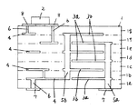
図1は、本発明に係る積層コンデンサ基板10の断面図である。尚、図において、容量成分を発生するコンデンサ部と該コンデンサ部と接続する回路部とを並設した例で説明する。
【0021】
図1において、1は積層セラミック基板であり、2は電子部品である。
【0022】
積層セラミック基板1には、コンデンサ部Xと多層回路部Yとが並設されておいる。また、積層セラミック基板1は、絶縁体セラミック層1a、誘電体セラミック層1b〜1f、絶縁体セラミック層1g(総称してセラミック層という)と、セラミック層1a〜1gの各層間には、前記容量部Xを構成する第1又は第2の電極層3a、3bが配置され、また、回路部Yを構成する内部配線4が配置されている。また、セラミック層1a〜1gには、前記容量部Xを構成する第1及び第2のビアホール導体5a、5bが形成され、また、また、回路部Yを構成するビアホール導体6が形成されている。
【0023】
また、積層セラミック基板1の主面には、コンデンサ部Xの端子電極7を含む回路部Yの表面配線(端子電極を含む)8が形成されている。図には示していないが、さらに、必要に応じて、厚膜抵抗体膜が形成されており、さらに、絶縁保護膜が電子部品2、端子電極7などを露出するように形成されている。
【0024】
ここで、積層セラミック基板1の表裏両主面となるセラミック層1a、1gをアルミナなどの絶縁体セラミック層で形成している。本来であれば、セラミック層1a〜1gを誘電体セラミック層とすべきであるが、例えば、積層セラミック基板1の主面に厚膜抵抗体膜を形成した場合、誘電体材料の一部(例えばチタニア成分、鉛成分など)が厚膜抵抗体膜に拡散して抵抗特性が不安定になりやすい。このため、厚膜抵抗体膜の抵抗特性を安定化するために絶縁体セラミック層を積層セラミック基板1の表裏両主面となるセラミック層1a、1gに用いている。また、基板の強度を考慮した場合にも有利となる。
【0025】
絶縁体セラミック層1a、1gは、比較的低い温度で焼成可能にするガラス−セラミック材料からなる。具体的なセラミック材料としては、クリストバライト、石英、コランダム(αアルミナ)、ムライト、コージライトなどが例示できる。また、ガラス材料として複数の金属酸化物を含むガラスフリットであり、焼成処理することによってコージェライト、ムライト、アノーサイト、セルジアン、スピネル、ガーナイト、ウイレマイト、ドロマイト、ペタライトやその置換誘導体の結晶を少なくとも1種類を析出するものであればよい。
【0026】
また、誘電体セラミック層1b〜1fは、セラミック材料としては、誘電率が高いBaTiO3 やPb4 Fe2 Nb2 O12などの誘電体セラミック材料が例示できる。これらセラミック層1a〜1gの厚みは例えば10〜100μm程度である。
【0027】
第1及び第2の電極層3a、3b、内部配線4、第1及び第2のビアホール導体5a、5b、ビアホール導体6は、Ag系(Ag単体、Ag−PdなどのAg合金)、Cu系(Cu単体、Cu合金)など導体からなり、第1及び第2の電極層3a、3b、内部配線4の厚みは8〜15μm程度である。尚、第1及び第2のビアホール導体5a、5b、ビアホール導体6の直径は任意な値とすることができるが、例えば第1及び第2のビアホール導体5a、5bの直径は250μm、ビアホール導体6の直径は、80μmである。
【0028】
端子電極7や表面配線8は、Ag系(Ag単体、Ag−PdなどのAg合金)、Cu系(Cu単体、Cu合金)など導体からなる。
【0029】
銅系の端子電極7、表面配線8は、マイグレーションなどが発生しないため高密度化にとっては重要な導体材料である。尚、銅系導体の場合には、焼きつけの条件が還元性雰囲気または中性雰囲気で行う必要があるが、積層セラミック基板1の焼成時に同時に焼きつけ処理するために、銀系導体を用いても構わない。
【0030】
電子部品2は、ICベアチップ、チップ抵抗器、チップコンデンサなどのチップ部品の他に、既に容器に収納されたIC、トランジスタ、発振部品などが挙げられる。尚、基板全体の高さを低くするために、基板表面に、電子部品2を収納するキャビティーを形成して、キビティー内に電子部品2を収納・配置してもよい。
【0031】
以上の構成では、例えば誘電体セラミック層1dを挟んで互いに対向する第1の電極層3aと第2の電極層3bとの間で所定容量成分が発生し、また誘電体セラミック層1eを挟んで互いに対向する第1の電極層3aと第2の電極層3bとの間で容量成分が発生する。そして、複数の第1の電極層3aは第1のビアホール導体5aによって共通的に接続され、複数の第2の電極層3bを第2のビアホール導体5bによって共通的に接続され、この容量部Xで発生した容量を端子電極7と第2ビアホール導体5bの一端と多層回路部Yとの接続部分との間で所定容量成分が導出することができる。
【0032】
この時、各電極3a、3bは直径が250μmと非常に大きい第1のビアホール導体5a、第2のビアホール導体体5bに接続され、この第1のビアホール導体5a、第2のビアホール導体体5bを介して所定容量が得られることになるため、各第1の電極層3aと第1のビアホール導体5aと接続の抵抗が、また、第2の電極層3bと第2のビアホール導体5bとの接続の抵抗が非常に小さくなり、また、端子電極7や多層回路部Yとの接続部分での接触抵抗が低下して、インダクタン値が非常に小さくなる。
【0033】
次に、積層セラミック基板1の製造方法を図2の工程の流れ図、図3(a)〜図3(f)の主要工程における断面図に基づいて説明する。
【0034】
まず、図2に示すように、予め、支持基板15を用意し、また、セラミック層1a〜1gとなるセラミックスリップ材を用意し、さらに電極層3a、3b、内部導体4、ビアホール導体5a、5b、6となる導電性ペーストを用意しておく。
【0035】
支持基板15は、例えば耐熱性樹脂、ガラス、セラミックなどなどが例示できる。
【0036】
セラミックスリップ材は、図1においては2種類のスリップ材が必要であり、例えば、焼成した後絶縁体セラミック層1a、1gとなる絶縁膜10a、10gを形成するためのスリップ材は、セラミック粉末、ガラス材料、光硬化可能なモノマー、バインダー、溶剤を均質混練して形成する。
【0037】
セラミック粉末は、クリストバライト、石英、コランダム(αアルミナ)、ムライト、コージライトなどの絶縁セラミック材料が例示できる。その平均粒径1.0〜6.0μm、好ましくは1.5〜4.0μmに粉砕したものを用いる。尚、セラミック材料は2種以上混合して用いられてもよい。特に、コランダムを用いた場合、コスト的に有利となる。
【0038】
ガラス材料として複数の金属酸化物を含むガラスフリットであり、焼成処理することによってコージェライト、ムライト、アノーサイト、セルジアン、スピネル、ガーナイト、ウイレマイト、ドロマイト、ペタライトやその置換誘導体の結晶を少なくとも1種類を析出するものであればよく、例えば、B2 O3 、SiO2 、Al2 O3 、ZnO、アルカリ土類酸化物を含むガラスフリットが挙げられる。この様なガラスフリットは、ガラス化範囲が広くまた屈伏点が600〜800℃付近にあるため、850〜1050℃程度の低温焼成に適し、内部導体3となる導体膜との焼結挙動が近似しているためである。尚、このガラスフリットの平均粒径は、1.0〜5.0μm、好ましくは1.5〜3.5μmである。
【0039】
上述のセラミック材料とガラス材料との構成比率は、850〜1050℃の比較的低温で焼成する場合には、セラミック材料が10〜60wt%、好ましくは30〜50wt%であり、ガラス材料が90〜40wt%、好ましくは70〜50wt%である。
【0040】
光硬化可能なモノマーは、比較的低温で且つ短時間の焼成工程で消失できるように熱分解性に優れたものであり、また、スリップ材の塗布・乾燥後の露光によって、光重合される必要があり、遊離ラジカルの形成、連鎖生長付加重合が可能で、2級もしくは3級炭素を有したモノマーが好ましく、例えば少なくとも1つの重合可能なエチレン系基を有するブチルアクリレート等のアルキルアクリレートおよびそれらに対応するアルキルメタクリレートが有効である。また、テトラエチレングリコールジアクリレート等のポリエチレングリコールジアクリレートおよびそれらに対応するメタクリレートなどが挙げられる。尚、光硬化可能なモノマーは、露光処理後の現像処理によって露光部分以外の部分が容易に除去できるように所定量添加される。例えば、固形成分(セラミック材料及びガラス材料) に対して5〜15wt%以下である。
【0041】
バインダーは、光硬化可能なモノマー同様に熱分解性の良好なものでなくてはならない。同時にスリップの粘性を決めるものである為、固形分との濡れ性も重視せねばならず、アクリル酸もしくはメタクリル酸系重合体のようなカルボキシル基、アルコール性水酸基を備えたエチレン性不飽和化合物が好ましい。添加量としては固形分に対して25wt%以下が好ましい。
【0042】
溶剤として、有機系溶剤、水系溶剤を用いることができる。尚、水系溶剤の場合、光硬化可能なモノマー及びバインダーは、水溶性である必要があり、モノマー及びバインダには、親水性の官能基、例えばカルボキシル基が付加されている。その付加量は酸価で表せば2〜300あり、好ましくは5〜100である。
【0043】
付加量が少ない場合は水への溶解性、固定成分の粉末の分散性が悪くなり、多い場合は熱分解性が悪くなるため、付加量は、水への溶解性、分散性、熱分解性を考慮して、上述の範囲で適宜付加される。
【0044】
何れの系のスリップ材においても光硬化可能なモノマー及びバインダは上述したように熱分解性の良好なものでなくてはならないが、具体的には600℃以下で熱分解が可能でなくてはならない。更に好ましくは500℃以下である。
【0045】
また、スリップ材には、増感剤、光開始系材料等を必要に応じて添加しても構わない。例えば、光開始系材料としては、ベンゾフェノン類、アシロインエステル類化合物などが挙げられる。
【0046】
また、焼成した後誘電体セラミック層1b〜1fとなる絶縁膜10b〜10fを形成するためのスリップ材は、誘電体セラミック粉末、光硬化可能なモノマー、バインダー、溶剤を均質混練して形成する。
【0047】
上述のセラミックスリップ材との相違点は、固形成分として、誘電体セラミック材料、例えば、BaTiO3 、Pb4 Fe2 Nb2 O12、TiO2 などの誘電体セラミック材料を用いた点である。
【0048】
焼成した後、電極層3a、3b、内部導体4、ビアホール導体5a、5b、6となる導体膜、導体を形成する導電性ペーストは、Ag系(Ag単体、Ag−PdなどのAg合金)、Cu系(Cu単体、Cu合金)など導体材料粉末、例えば銀系粉末と、低融点ガラス成分と、有機バインダーと有機溶剤とを均質混練したものが用いられる。尚、上述の導電性ペースト中に、セラミックスリップ材に用いた光硬化モノマーを添加し、各導体膜を印刷し、乾燥した後、露光処理によって光硬化させても構わない。 これは、後述するように、導体膜上にセラミック層となる絶縁膜上の全面に塗布して、この絶縁膜に貫通凹部を形成するべく、露光、現像処理した時に、絶縁膜の貫通凹部の下部開口から露出する既に形成した導体膜もが除去されないようにするためである。尚、絶縁膜の現像処理に用いる現像液が、露光処理されていない絶縁膜のみを除去し、既に形成した導体や導体膜などを除去しないようにその成分や濃度を制御すれば、導電性ペーストに光硬化モノマーを用いる必要がなく、且つ導体、導体膜に対する露光処理を省略できる。
【0049】
上述のように、支持基板15、セラミック層1a〜1gとなるセラミックスリップ材、内部導体3となる導電性ペーストの準備を施した後、積層セラミック基板1となる積層体を形成する工程となる。
【0050】
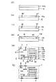
まず、図3(a)に示すように、(1)の工程として、支持基板15上に絶縁体セラミック層1aとなる絶縁膜10aを形成する。具体的には、セラミックスリップ材を40〜120μm程度になるように塗布、乾燥して形成する。
【0051】
スリップ材の塗布方法として、例えば、ドクターブレード法(ナイフコート法)、ロールコート法、印刷法などが挙げられる。特に塗布後の絶縁膜の表面が平坦化することが容易なドクターブレード法などが好適である。尚、塗布方法に応じて溶剤の添加量が調整され、所定粘度に調整される。
【0052】
乾燥方法としては、バッチ式乾燥炉、インライン式乾燥炉を用いて行われ、乾燥条件は、120℃以下が望ましい。また、急激な乾燥は、表面にクラックを発生される可能性があるため、急加熱を避けることが重要となる。
【0053】
次に、図3(b)に示すように、(2)の工程の前工程であるスリップ材を塗布・乾燥した絶縁膜10aを選択的な露光処理して、絶縁膜10aの所定位置、即ち、第1及び第2のビアホール導体5a、5bとなる位置に、貫通凹部50(実際には、支持基体15の存在のため凹部形状となる)となる溶化部50’を形成する。尚、この基板内に回路部を構成する図1の場合、この工程で同時に、ビアホール6となる位置に、貫通凹部60となる溶化部60’を形成する。
【0054】
具体的には、絶縁膜10a中に含まれる光硬化モノマーが、光重合されるネガ型であるため、貫通凹部50、60となる溶化部50’、60’のみが露光光が照射されないような所定パターンを有するフォトターゲットを、絶縁膜10a上に載置、又は近接配置して、低圧、高圧、超高圧の水銀灯系の露光光を照射する。尚、露光条件は、15〜20J/cm2 の露光光を約15〜30秒程度照射して行う。これにより、絶縁膜10aの第1及び第2のビアホール導体5a、5b、ビアホール導体6となる部分以外は、光硬化可能なモノマーの光重合反応を起し、光硬化されることになる。尚、露光装置は所謂写真製版技術に用いられる一般的なものでよい。
【0055】
そして、図3(c)に示すように、(2)の工程の後工程として、露光処理した絶縁膜10aを現像処理し、溶化部50’、60’を除去して、貫通凹部50、60を形成する。これにより、貫通凹部50、60の下部開口には、支持基板15の一部が露出することになる。
【0056】
具体的には、現像処理として、クロロセン、1,1,1−トリクロロエタン、アルカリ現像溶剤を例えばスプレー現像法やパドル現像法によって、溶化部40’に噴射したり、接触したりして、現像処理を行う。その後、必要に応じて洗浄及び乾燥を行なう。
【0057】
次に、図3(d)に示すように、(3)の工程として、現像処理して絶縁膜10aの貫通凹部50、60内に、第1、第2のビアホール導体5a、5bとなる導体51a、51b、ビアホール導体6となる導体61を導電性ペーストの充填によって形成する。
【0058】
続いて、(4)の工程として、絶縁膜10a上に、セラミック層1aとセラミック層1bとの間に配置される第1の電極層3aとなる導体膜31aを形成する。尚、この基板内に回路部を構成する図1の場合、この工程で同時に、内部配線4となる導体膜41を導電性ペーストの印刷によって形成する。
【0059】
上述の(3)のビアホール導体となる導体を形成する工程と(4)の電極層となる導体膜、内部配線となる導体膜を形成する工程を同一のスクリーン印刷で同時に行うこともできる。
【0060】
以上で、一連の(1)〜(4)の各工程が終了する。
【0061】
次に、セラミックスリップ材を誘電体セラミック層となるセラミックスリップ材に代えて、上述の(1)の工程を繰り返して、誘電体セラミック層1bとなる絶縁膜10bを形成し、続いて、(2)の工程を行って、絶縁膜10bに第1、第2のビアホール導体5aと貫通凹部50、ビアホール導体6と貫通凹部60を形成し、続いて、(3)(4)の工程を行って、貫通凹部50及び貫通凹部60に導電性ペーストを充填して導体51a、51b、61を形成するとともに、絶縁膜10b上に誘電体セラミック層1bと誘電体セラミック層1cとの間に配置される電極層3bとなる導体膜31b、内部配線4となる導体膜41を形成する。
【0062】
同様に、誘電体セラミック層1c〜誘電体セラミック層1fとなる絶縁膜10c〜10f、絶縁膜10c〜10fに形成される導体51a、51b、61、絶縁膜10c〜10f上に形成される導体膜31a、31b、41を形成する。
【0063】
最後に、また、スリップ材を代えて、(1)の工程を行って、最上層の絶縁体セラミック層1gとなる絶縁膜10gを形成し、続いて(2)の工程を行って、絶縁膜10g中にビアホール導体6となる貫通凹部60を形成し、(3)工程のみを行って、貫通凹部60内にビアホール導体6となる導体61を形成する。絶縁膜10gのビアホール導体6は基板の表面に露出するものであるため、その後現像処理されることがない場合は、光硬化を行う露光処理は省略される。
【0064】
次に、図3(e)に示すように、支持基板15を分離して、積層コンデンサ基板10の寸法で分割できるようにプレス成型によって分割溝を形成し、一体的な焼結を行う。
【0065】
焼結は、脱バインダ過程と焼成過程からなる。脱バインダ過程は、絶縁膜10a〜10g、第1の電極層3aとなる導体膜31a、第2の電極層3bとなる導体膜31b、内部配線4となる導体膜41、第1のビアホール導体5aとなる導体51a、第2のビアホール導体5bとなる導体51b、ビアホール導体6となる導体61に含まれる有機成分を焼失するためのものであり、焼結過程の例えば600℃以下の温度領域で行われる。
【0066】
また、焼成過程は、絶縁膜10a〜10gのガラス成分を充分に軟化させて、セラミック粉末の粒界に均一に分散させ、積層セラミック基板1に一定強度を与え、同時に、導体膜31a、31b、41、各ビアホール導体となる導体51a、51b、61の銀系粉末を粒成長させて、低抵抗化させるとともに、絶縁層1a〜1gと一体化させるものであり、酸化性雰囲気又は中性雰囲気でピーク温度850〜1050℃で行われる。
【0067】
これにより、絶縁膜10a〜10gはセラミック層1a〜1gとなり、導体膜導体膜31a、31b、41は夫々、第1の電極層3a、第2の電極層3b、内部配線4となり、導体51a、51b、61は第1のビアホール導体導体5a、第2のビアホール導体5b、ビアホール導体6となる。
【0068】
尚、支持基板15として、セラミック基体を用いる場合は、そのまま積層セラミック基板1の一部として用いることができる。この時、支持基板15上に内部配線を形成しておいてもよい。
【0069】
次に、図3(f)に示すように、基板の両主面に、銅系導電性ペーストで端子端子電極7、表面配線8となる各導体膜を印刷形成し、その後、乾燥・焼成を行う。
【0070】
ここで、銅系の端子電極7、表面配線8と銀系導体のビアホール導体6とが接合することになる。このため、銀と銅との共晶温度を考慮して、銅系の表面配線7として、低温(例えば780℃以下)焼成可能な銅系導電性ペーストをスクリーン印刷して、銅の酸化を防止するため、還元性雰囲気や中性雰囲気中で行うことが重要である。
【0071】
その後、必要に応じて、厚膜抵抗膜や保護膜などを焼きつけを行い、分割溝にそって個々の基板の大きさに分割を行い、積層セラミック基板1が達成される。
【0072】
さらに、電子部品2を、積層セラミック基板1の表面に半田接合する。
【0073】
以上のように、上述の製造方法によれば、複数の第1の電極層3aを共通的に接続する第1のビアホール導体5a、複数の第2の電極層3bを共通的に接続する第2のビアホール導体5bは、セラミック層1a〜1gとなる絶縁膜10a〜10gに露光・現像処理によって形成された貫通凹部50に導電性ペーストを充填して形成される。このため、従来、非常に困難とされていたグリーンシートのスルーホールへの導電性ペーストの充填保持が不要となりため、特に、250μm程度の径であっても安定したビアホール導体5a、5bを形成することができる。
【0074】
しかも、第1のビアホール導体5a、第2のビアホール導体5bを直径、形状・また異なるセラミック層に形成されたビアホール導体5a、5bとの接続位置も、上述の精度の高い露光処理によってのみ決まるため、直径、形状を任意とすることができ、ビアホール導体5a、5bの接続位置ずれなどのが一切発生せず、ビアホール導体での接続抵抗が低く、且つ信頼性の高い、即ち、インダクタンス値の非常に低いコンデンサを簡単に形成することが可能となる。
【0075】
また、各絶縁膜10a〜10gの形成が、スリップ材の塗布によって行われるため、その膜厚の制御が容易であり、セラミック層1a〜1gの誘電率に応じたもっとも最適な膜厚とすることができる。
【0076】
また、この絶縁膜10a〜10gを形成した時の表面は、下部に配置された電極層3a、3bや内部配線4のパターン形状、積層数の関わらず、常に均一な平坦面となる。このため、この絶縁膜10a〜10eの表面に電極層3a、3bとなる導体膜31a、31bや内部配線4となる導体膜41、表面配線8などを形成するにあたり、確実に行えることになる。
【0077】
また、インダクタンス値の低い容量部Xと同一の基板内に、この容量部Xの形成工程と同時に、容量部Xと接続する回路部Yを形成することができるため、特に高速動作の回路と一体化することにより、インダクタンス値の低い容量部Xの特性を充分に奏することができる。
【0078】
尚、回路部Xにおいても、ビアホール導体6の直径、形状は任意に設定できるため、回路の電源ライン、アースラインなど大電流の流れるビアホール導体6の低抵抗化が容易に行えることになる。
【0079】
尚、上述の実施例において、第1の電極層3aと第2の電極層3b、内部配線4、第1、第2のビアホール導体5a、5b、ビアホール導体6の導体材料と、基板表面の表面配線8、端子電極7の導体材料とが異種の導体材料で形成されているが、少なくとも同一条件で焼成できる導体材料を用いることにより、端子電極7、表面配線8の焼きつけ工程を、積層セラミック基板1の焼成工程前に行い、絶縁膜10a〜10gと全ての導体とを同時に焼成することもできる。
【0080】
また、図1に示す積層コンデンサ基板10においては、基板の裏面側主面には端子電極7や表面配線8を形成しているため、(1)の工程である最下部のセラミック層1aとなる絶縁膜10aの形成工程を行った後に、(2)の工程であるビアホール導体となる貫通凹部50、60を形成するための露光・現像処理工程をおこなっているが、基板の裏面側主面には端子電極7や表面配線8を形成しない場合は、絶縁膜10aを形成した後、(2)の工程を省略して、(3)の工程である導体膜の形成工程を行っても構わない。
【0081】
さらに、セラミック層の積層数は7層構造であるが、容量値に応じて、積層数を任意に設定することができ、また、容量部Xが1つだけではなしに、複数発生するようにしても構わない。
【0082】
実施例では、積層コンデンサ基板10内に容量部Xと回路部Yとを並設しているが、1つ又は複数の容量部Xのみで積層コンデンサ基板10を構成、即ち、積層コンデンサとしても構成しても構わない。この時、セラミック層として全て誘電体セラミック層のみで構成し、その積層セラミック基板1の主面には、第1及び第2のビアホール導体5a、5bと接続する島状の端子電極を形成する。
【0083】
【発明の効果】
以上のように本発明によれば、セラミック層となる絶縁膜を光硬化モノマーを含有するスリップ材を用いて、順次塗布によって形成し、ビアホール導体となる貫通孔を絶縁膜の選択的な露光・現像処理によって形成し、ビアホール導体となる導体、電極層となる導体膜を導電性ペーストの印刷などで形成している。 従って、特にビアホール導体の直径を任意に設定することができるため、インダクタンス値が低く、且つ接続信頼性が高い積層コンデンサ基板が非常に簡単に形成できる。
【0084】
また、積層コンデンサ基板内にこのコンデンサと接続する回路を、コンデンサの形成工程と同時に形成することができるため、積層コンデンサ基板内に回路部を並設することにより、インダクタンス値が低い、即ち高速動作する回路に対応することができるというコンデンサの特性を充分に引き出すことができる。
【図面の簡単な説明】
【図1】本発明に係る積層コンデンサ基板の断面図である。
【図2】本発明の積層コンデンサ基板の製造を説明するための工程図である。
【図3】(a)〜(f)は本発明の積層コンデンサ基板の製造の主要工程における断面図である。
【図4】従来の低インダクタン型積層コンデンサの概略平面図である。
【符号の説明】
10・・・・・積層コンデンサ基板
1・・・・・・・積層セラミック基板
1a〜1g・・・セラミック層
10a〜10g・・・絶縁膜
2・・・・・・・電子部品
3a・・・・・・第1の電極層
3b・・・・・・第2の電極層
4・・・・・・・内部配線
5a・・・・・・第1のビアホール導体
5b・・・・・・第2のビアホール導体
6・・・・・・・ビアホール導体
7・・・・・・・端子電極
8・・・・・・・表面配線
31a・・・・・・第1の電極層となる導体膜
31b・・・・・・第2の電極層となる導体膜
41・・・・・・・内部配線となる導体膜
51a・・・・・・第1のビアホール導体となる導体
51b・・・・・・第2のビアホール導体となる導体
61・・・・・・ビアホール導体となる導体[0001]
[Industrial application fields]
The present invention relates to a method for manufacturing a multilayer capacitor substrate in which a dielectric ceramic layer is sandwiched between a first electrode layer and a second electrode layer.
[0002]
[Prior art]
Conventionally, a multilayer chip capacitor is formed by laminating a plurality of dielectric ceramic green sheets as ceramics in which a conductor film serving as an internal electrode layer is formed in a chip-shaped region, and cutting the chip according to the chip region, followed by a firing process. The terminal electrode was formed in the both end surfaces which a laminated body opposes. The internal electrode layer includes a first internal electrode layer formed from one end surface side so that the end side is exposed on one end face of the laminate, and the other end face is exposed on the other end face of the laminate. It consists of a second internal electrode layer formed from the end face side, and these layers are alternately stacked via ceramic layers.
[0003]
Usually, in the multilayer chip capacitor, the connection between the internal electrode layer and the terminal electrode is made depending on the thickness of the internal electrode layer (for example, 2 to 3 μm), so that the connection resistance at this connection portion increases. In particular, when such a multilayer chip capacitor is used for a switching circuit that operates at a high speed, an inductance component increases at the connection portion between the internal electrode and the terminal electrode (for example, 0.8 nH), and does not follow the high-speed operation. It was a thing.
[0004]
Therefore, as a structure for reducing the inductance component, the
[0005]
[Problems to be solved by the invention]
However, when the multilayer chip capacitor shown in FIG. 4 is manufactured, the dielectric green sheet to be the
[0006]
However, the thickness of the dielectric green sheet to be the
[0007]
In addition, a multilayer chip capacitor having a low inductance value needs to be directly connected to, for example, a circuit forming a switching circuit, and mounting a single multilayer chip capacitor on a pepper wiring board has an effect as a capacitor having a low inductance value. It is difficult to play well.
[0008]
The present invention has been devised in view of the above-described problems, and an object thereof is to provide a method for easily manufacturing a multilayer capacitor substrate having a low inductance value regardless of the diameter of the via-hole conductor. .
[0009]
Another object is to provide a method of manufacturing a multilayer capacitor substrate that can be directly connected to other circuits in order to sufficiently exhibit the action of the low-inductance multilayer capacitor substrate.
[0010]
[Means for Solving the Problems]
According to the present invention, a plurality of dielectric ceramic layers are provided between the first insulator ceramic layer and the second insulator ceramic layer, and the first electrode layer and the second electrode sandwiching the dielectric ceramic layer are provided. The electrode layers are alternately stacked, and the first electrode layer and the second electrode layer are connected to each other through first and second via-hole conductors formed on the plurality of dielectric ceramic layers. A capacitor portion, a plurality of internal wirings connected to the capacitor portion and sandwiching the plurality of dielectric ceramic layers, and the plurality of dielectric ceramic layers and the second insulator connecting the plurality of internal wires A method for manufacturing a multilayer capacitor substrate, comprising: a third via-hole conductor formed in a ceramic layer; a surface wiring formed on the second insulator ceramic layer; and a circuit portion comprising an electronic component connected to the surface wiring. Because
A method for forming the multilayer capacitor substrate is as follows.
Applying a ceramic slip material containing a photocurable monomer on a support substrate to form an insulating film to be the first insulating ceramic layer;
A conductive paste is printed on the surface of the insulating film to be the first insulator ceramic layer to form the conductive film to be the first or second electrode layer, and the conductive film to be the internal wiring is formed. After sequentially carrying out the process
(1) A step of applying a ceramic slip material containing a photocurable monomer to form an insulating film to be the dielectric ceramic layer;
(2) The insulating film to be the dielectric ceramic layer is selectively exposed and developed to form a third through hole at a position to be the third via hole conductor, and the first and second via holes. Forming first and second through holes at positions to be conductors;
(3) filling each through hole of the insulating film to be the dielectric ceramic layer with a conductive paste to form a conductor to be the first to third via-hole conductors;
(4) A conductive paste is printed on the surface of the insulating film to be the dielectric ceramic layer so that a part of the conductive paste is connected to the conductor filled in the first or second through hole, and the first or second is printed. Forming a conductor film to be an electrode layer of the first and forming a conductor film to be the internal wiring by printing so as to be connected to the conductor filled in the third through-hole,
After sequentially repeating the above steps (1) to (4),
Applying a ceramic slip material containing a photocurable monomer to form an insulating film to be the second insulating ceramic layer;
A step of selectively exposing and developing the insulating film to be the second insulator ceramic layer to form a third through hole at a position to be the third via hole conductor;
After sequentially performing the step of filling the third through hole with a conductive paste and forming a conductor to be a third via-hole conductor,
Separating the support substrate to form a laminate in which the insulating film, the conductor, and the conductor film are integrated; and
The laminated body is fired to form the first and second insulator ceramic layers, the dielectric ceramic layer, the first to third via hole conductors, the first and second electrode layers, and the internal wiring. Forming, and
Forming the surface wiring on the surface of the second insulator ceramic layer so that a part thereof is connected to the third via-hole conductor;
Connecting the electronic component to the surface wiring; and
A method for manufacturing a multilayer capacitor substrate, comprising:
[0011]
Although the through hole penetrates the insulating film, the lower opening of the through hole is closed by the already formed conductor film or conductor before the insulating film is formed. Since it has a “concave” shape, it is expressed as a “penetrating recess” in the manufacturing method of the present invention in order to distinguish it from a through hole of a manufacturing method using a conventional green sheet.
[0012]
[Action]
In the present invention, since the insulating film to be the dielectric ceramic layer is formed by applying a ceramic slip material containing a photocurable monomer and drying it, the thickness of the ceramic layer can be controlled very easily.
[0013]
Further, since the through recesses to be the first and second via hole conductors formed in the insulating film to be the ceramic layer are formed by selective exposure / development processing of the insulating film, any shape and size, for example, 250 μm Thus, a highly accurate through recess can be easily created.
[0014]
In addition, since the conductors serving as the first and second via-hole conductors are formed by filling the above-described through recesses, the conductors can be stably formed, and the through holes formed in the conventional green sheet can be formed. The filled conductive paste is never filled out.
[0015]
In forming the first or second electrode layer, since the insulating film to be a formation surface is formed by applying and drying a slip material, the formation surface can always be a flat surface. Alternatively, the second electrode layer can be formed stably.
[0016]
Therefore, the above steps (1) to (4) are sequentially repeated, but since the positioning of the via-hole conductor is actually defined by highly accurate exposure / development processing, conventional green sheets are laminated. The first and second electrode layers are connected by a relatively large via-hole conductor and can be led out to the outside, so that a low-inductance multilayer capacitor substrate is obtained. .
[0017]
In forming the above-described multilayer capacitor substrate, an external circuit connected to the capacitor can be easily formed on the multilayer capacitor substrate. That is, when the first or second electrode layer is formed, a predetermined wiring pattern constituting an external circuit connected to the capacitance component is formed, and when the first and second via holes are simultaneously formed, the wiring pattern is formed between the wiring patterns. A via-hole conductor to be connected can be formed at the same time.
[0018]
Therefore, it is possible to provide a circuit-integrated multilayer capacitor substrate that can sufficiently exhibit the effect of a low-inductance multilayer capacitor.
[0019]
【Example】
The present invention will be described below with reference to the drawings.
[0020]
FIG. 1 is a cross-sectional view of a multilayer capacitor substrate 10 according to the present invention. In the figure, an example in which a capacitor unit that generates a capacitance component and a circuit unit connected to the capacitor unit are arranged in parallel will be described.
[0021]
In FIG. 1, 1 is a multilayer ceramic substrate, and 2 is an electronic component.
[0022]
The multilayer
[0023]
Further, on the main surface of the multilayer
[0024]
Here, the ceramic layers 1a and 1g which are the front and back main surfaces of the multilayer
[0025]
The insulator ceramic layers 1a and 1g are made of a glass-ceramic material that enables firing at a relatively low temperature. Specific examples of the ceramic material include cristobalite, quartz, corundum (α alumina), mullite, and cordierite. Further, it is a glass frit containing a plurality of metal oxides as a glass material, and at least one crystal of cordierite, mullite, anorthite, serdian, spinel, garnite, willemite, dolomite, petalite and substituted derivatives thereof is obtained by firing treatment. Any material that precipitates the type may be used.
[0026]
The dielectric
[0027]
The first and second electrode layers 3a and 3b, the
[0028]
The
[0029]
The copper-based
[0030]
Examples of the
[0031]
In the above configuration, for example, a predetermined capacitance component is generated between the first electrode layer 3a and the
[0032]
At this time, the
[0033]
Next, a method for manufacturing the multilayer
[0034]
First, as shown in FIG. 2, a
[0035]
Examples of the
[0036]
The ceramic slip material requires two types of slip materials in FIG. 1. For example, the slip material for forming the insulating
[0037]
Examples of the ceramic powder include insulating ceramic materials such as cristobalite, quartz, corundum (α alumina), mullite, and cordierite. The average particle diameter is 1.0 to 6.0 μm, preferably 1.5 to 4.0 μm. Two or more ceramic materials may be mixed and used. In particular, use of corundum is advantageous in terms of cost.
[0038]
It is a glass frit containing a plurality of metal oxides as a glass material, and at least one kind of crystals of cordierite, mullite, anorthite, serdian, spinel, garnite, willemite, dolomite, petalite and substituted derivatives thereof are obtained by firing treatment. Any material that precipitates, such as B 2 O Three , SiO 2 , Al 2 O Three , ZnO, and a glass frit containing an alkaline earth oxide. Since such a glass frit has a wide vitrification range and a yield point in the vicinity of 600 to 800 ° C., it is suitable for low-temperature firing at about 850 to 1050 ° C. and approximates the sintering behavior with the conductor film serving as the inner conductor 3. It is because it is doing. In addition, the average particle diameter of this glass frit is 1.0-5.0 micrometers, Preferably it is 1.5-3.5 micrometers.
[0039]
When the ceramic material and the glass material are sintered at a relatively low temperature of 850 to 1050 ° C., the ceramic material is 10 to 60 wt%, preferably 30 to 50 wt%, and the glass material is 90 to 90%. It is 40 wt%, preferably 70-50 wt%.
[0040]
The photo-curable monomer is excellent in thermal decomposability so that it can be disappeared at a relatively low temperature and in a short baking process, and it must be photopolymerized by exposure after application and drying of the slip material. A monomer having secondary or tertiary carbon is preferable, and free radical formation and chain growth addition polymerization are possible. For example, alkyl acrylate such as butyl acrylate having at least one polymerizable ethylene group and Corresponding alkyl methacrylates are effective. In addition, polyethylene glycol diacrylates such as tetraethylene glycol diacrylate and methacrylates corresponding to them can be used. The photocurable monomer is added in a predetermined amount so that a portion other than the exposed portion can be easily removed by the development processing after the exposure processing. For example, it is 5-15 wt% or less with respect to a solid component (ceramic material and glass material).
[0041]
The binder must be as thermally decomposable as the photocurable monomer. At the same time, because it determines the viscosity of the slip, we must also focus on the wettability with the solid content. Ethylenically unsaturated compounds with carboxyl groups and alcoholic hydroxyl groups such as acrylic acid or methacrylic acid polymers are used. preferable. As addition amount, 25 wt% or less is preferable with respect to solid content.
[0042]
As the solvent, an organic solvent or an aqueous solvent can be used. In the case of an aqueous solvent, the photocurable monomer and binder must be water-soluble, and a hydrophilic functional group such as a carboxyl group is added to the monomer and binder. The addition amount is 2 to 300, preferably 5 to 100 in terms of acid value.
[0043]
If the added amount is small, the solubility in water and the dispersibility of the fixed component powder will be poor, and if it is large, the thermal decomposability will be poor. Therefore, the added amount is soluble in water, dispersible, and thermally decomposable. Is added as appropriate within the above-mentioned range.
[0044]
In any system of slip material, the photocurable monomer and binder must have good thermal decomposability as described above. Specifically, thermal decomposition must be possible at 600 ° C. or lower. Don't be. More preferably, it is 500 degrees C or less.
[0045]
Moreover, you may add a sensitizer, a photoinitiating system material, etc. to a slip material as needed. For example, examples of the photoinitiating material include benzophenones and acyloin ester compounds.
[0046]
The slip material for forming the insulating films 10b to 10f to be the dielectric
[0047]
The difference from the above ceramic slip material is that as a solid component, a dielectric ceramic material, for example, BaTiO. Three , Pb Four Fe 2 Nb 2 O 12 TiO 2 This is a point using a dielectric ceramic material such as.
[0048]
After firing, the conductive layers that form the
[0049]
As described above, after preparing the
[0050]
First, as shown in FIG. 3A, as a step (1), an insulating
[0051]
Examples of the slip material coating method include a doctor blade method (knife coating method), a roll coating method, and a printing method. In particular, a doctor blade method or the like that can easily flatten the surface of the insulating film after application is suitable. In addition, the addition amount of a solvent is adjusted according to a coating method, and is adjusted to predetermined viscosity.
[0052]
As a drying method, a batch type drying furnace or an in-line type drying furnace is used, and the drying condition is desirably 120 ° C. or lower. Moreover, since rapid drying may cause cracks on the surface, it is important to avoid rapid heating.
[0053]
Next, as shown in FIG. 3B, the insulating
[0054]
Specifically, since the photocurable monomer contained in the insulating
[0055]
Then, as shown in FIG. 3C, as a subsequent step of the step (2), the exposed insulating
[0056]
Specifically, as the development processing, chlorocene, 1,1,1-trichloroethane, and an alkali developing solvent are sprayed or contacted to the solubilized
[0057]
Next, as shown in FIG. 3 (d), in the step (3), a conductor that becomes the first and second via-hole conductors 5a and 5b in the through
[0058]
Subsequently, as a step (4), a conductor film 31a to be the first electrode layer 3a disposed between the ceramic layer 1a and the
[0059]
The step (3) of forming a conductor to be a via-hole conductor and the step (4) of forming a conductor film to be an electrode layer and a conductor film to be an internal wiring can be simultaneously performed by the same screen printing.
[0060]
With the above, a series of steps (1) to (4) are completed.
[0061]
Next, the ceramic slip material is replaced with a ceramic slip material to be a dielectric ceramic layer, and the above-described step (1) is repeated to form the insulating film 10b to be the dielectric
[0062]
Similarly, insulating films 10c to 10f to be the dielectric ceramic layers 1c to 1f,
[0063]
Finally, instead of the slip material, the step (1) is performed to form the insulating film 10g to be the uppermost insulator ceramic layer 1g, and then the step (2) is performed to obtain the insulating film. A through
[0064]
Next, as shown in FIG. 3 (e), the
[0065]
Sintering consists of a binder removal process and a firing process. The binder removal process includes the insulating
[0066]
In the firing process, the glass components of the insulating
[0067]
Thereby, the insulating
[0068]
When a ceramic substrate is used as the
[0069]
Next, as shown in FIG. 3 (f), the conductor films to be the terminal
[0070]
Here, the copper-based
[0071]
Thereafter, if necessary, a thick film resistance film, a protective film, or the like is baked and divided into individual substrate sizes along the dividing grooves, whereby the multilayer
[0072]
Further, the
[0073]
As described above, according to the manufacturing method described above, the first via-hole conductor 5a that commonly connects the plurality of first electrode layers 3a and the second that commonly connects the plurality of
[0074]
Moreover, since the first via hole conductor 5a and the second via hole conductor 5b have diameters, shapes, and positions where the via hole conductors 5a and 5b formed in different ceramic layers are determined only by the high-precision exposure process described above. The diameter and shape can be set arbitrarily, there is no displacement of the via hole conductors 5a and 5b, the connection resistance at the via hole conductor is low, and the reliability is high, that is, the inductance value is extremely high. It is possible to easily form a low capacitor.
[0075]
In addition, since the insulating
[0076]
Further, the surface when the insulating
[0077]
In addition, since the circuit part Y connected to the capacitor part X can be formed simultaneously with the process of forming the capacitor part X in the same substrate as the capacitor part X having a low inductance value, it is particularly integrated with a circuit operating at high speed. As a result, the characteristics of the capacitance part X having a low inductance value can be sufficiently achieved.
[0078]
Also in the circuit portion X, the diameter and shape of the via-
[0079]
In the above-described embodiment, the first electrode layer 3a and the
[0080]
Further, in the multilayer capacitor substrate 10 shown in FIG. 1, since the
[0081]
Furthermore, although the number of laminated ceramic layers is a seven-layer structure, the number of laminated layers can be arbitrarily set according to the capacitance value, and more than one capacitor portion X is generated, and a plurality of ceramic layers are generated. It doesn't matter.
[0082]
In the embodiment, the capacitance part X and the circuit part Y are arranged in parallel in the multilayer capacitor substrate 10, but the multilayer capacitor substrate 10 is configured by only one or a plurality of capacitance parts X, that is, also configured as a multilayer capacitor. It doesn't matter. At this time, the ceramic layers are all composed only of dielectric ceramic layers, and island-like terminal electrodes connected to the first and second via-hole conductors 5a and 5b are formed on the main surface of the multilayer
[0083]
【The invention's effect】
As described above, according to the present invention, the insulating film to be the ceramic layer is formed by sequential application using the slip material containing the photocuring monomer, and the through hole to be the via-hole conductor is selectively exposed to the insulating film. Formed by development processing, a conductor to be a via-hole conductor and a conductor film to be an electrode layer are formed by printing a conductive paste or the like. Therefore, in particular, since the diameter of the via-hole conductor can be arbitrarily set, a multilayer capacitor substrate having a low inductance value and high connection reliability can be formed very easily.
[0084]
In addition, since the circuit connected to this capacitor can be formed in the multilayer capacitor substrate at the same time as the capacitor formation process, the inductance is low, that is, high-speed operation by arranging the circuit part in the multilayer capacitor substrate. Therefore, it is possible to sufficiently bring out the characteristics of the capacitor that can correspond to the circuit to be operated.
[Brief description of the drawings]
FIG. 1 is a cross-sectional view of a multilayer capacitor substrate according to the present invention.
FIG. 2 is a process diagram for explaining the production of the multilayer capacitor substrate of the present invention.
FIGS. 3A to 3F are cross-sectional views in the main steps of manufacturing the multilayer capacitor substrate of the present invention. FIGS.
FIG. 4 is a schematic plan view of a conventional low-inductance multilayer capacitor.
[Explanation of symbols]
10 ... Multilayer capacitor board
1 ..... Multilayer ceramic substrate
1a to 1g ... ceramic layer
10a-10g ... insulating film
2 .... Electronic parts
3a .... First electrode layer
3b .... Second electrode layer
4 .... Internal wiring
5a... First via hole conductor
5b .... Second via hole conductor
6 .... via hole conductor
7 ・ ・ ・ ・ ・ ・ ・ ・ ・ ・ ・ Terminal electrode
8 .... surface wiring
31a... Conductor film serving as first electrode layer
31b... Conductor film to be second electrode layer
41... Conductor film for internal wiring
51a... Conductor serving as first via-hole conductor
51b... Conductor serving as second via hole conductor
61... Conductor to be a via-hole conductor
Claims (1)
前記積層コンデンサ基板の形成方法が
支持基板上に、光硬化可能なモノマーを含有するセラミックスリップ材を塗布して前記第1の絶縁体セラミック層となる絶縁膜を形成する工程と、
該第1の絶縁体セラミック層となる絶縁膜の表面に導電性ペーストを印刷して前記第1又は第2の電極層となる導電膜を形成するとともに、前記内部配線となる導電膜を形成する工程とを順次行った後、
(1)光硬化可能なモノマーを含有するセラミックスリップ材を塗布して前記誘電体セラミック層となる絶縁膜を形成する工程と
(2)前記誘電体セラミック層となる絶縁膜を選択的に露光・現像処理して、第3のビアホール導体となる位置に、第3の貫通孔を形成するとともに、第1及び第2のビアホール導体となる位置に、第1及び第2の貫通孔を形成する工程、
(3)前記誘電体セラミック層となる絶縁膜の各貫通孔に導電性ペーストを充填して前記第1乃至第3のビアホール導体となる導体とを形成する工程と、
(4)前記誘電体セラミック層となる絶縁膜の表面に導電性ペーストを、一部が前記第1または第2の貫通孔に充填した導体と接続するように印刷して前記第1又は第2の電極層となる導体膜を形成するとともに、前記第3の貫通孔に充填した導体と接続するように印刷して前記内部配線となる導体膜を形成する工程、
の上述の(1)乃至(4)の各工程を順次繰り返した後、
光硬化可能なモノマーを含有するセラミックスリップ材を塗布して前記第2の絶縁体セラミック層となる絶縁膜を形成する工程と、
該第2の絶縁体セラミック層となる絶縁膜を選択的に露光・現像処理して、第3のビアホール導体となる位置に第3の貫通孔を形成する工程と、
該第3の貫通孔に導電性ペーストを充填して第3のビアホール導体となる導体を形成する工程とを順次行った後、
前記支持基板を分離して、絶縁膜、導体及び導体膜が一体化された積層体を形成する工程と、
該積層体を焼成処理して、前記第1及び第2の絶縁体セラミック層、前記誘電体セラミック層、前記第1乃至第3のビアホール導体、前記第1及び第2の電極層及び内部配線を形成する工程と、
前記第2の絶縁体セラミック層の表面に、一部が第3のビアホール導体と接続するように前記表面配線を形成する工程と、
前記表面配線に前記電子部品を接続する工程と
を有することを特徴とする積層コンデンサ基板の製造方法。 First insulator having a ceramic layer and a second insulating ceramic layer a plurality of dielectric ceramic layers between, alternating with the first electrode layer and the second electrode layer I interposed do the dielectric ceramic layers A capacitor portion formed by stacking a plurality of the first electrode layers and the second electrode layers through the first and second via hole conductors formed on the plurality of dielectric ceramic layers; connected to said capacitor portion, and a plurality of internal wirings sandwiching the plurality of dielectric ceramic layers were formed on the plurality of dielectric ceramic layers and second insulating ceramic layers for connecting the internal wiring of the plurality of A method of manufacturing a multilayer capacitor substrate having a third via-hole conductor, a surface wiring formed on the second insulator ceramic layer, and a circuit portion comprising an electronic component connected to the surface wiring ,
The method for forming the multilayer capacitor substrate includes a step of applying a ceramic slip material containing a photocurable monomer on a support substrate to form an insulating film to be the first insulator ceramic layer ;
A conductive paste is printed on the surface of the insulating film to be the first insulator ceramic layer to form the conductive film to be the first or second electrode layer, and the conductive film to be the internal wiring is formed. After sequentially performing the process,
(1) process and (2) by applying a ceramic slip material to form an insulating film serving as the dielectric ceramic layer containing a photocurable monomer selectively exposed and the dielectric ceramic layer to become an insulating film A step of developing to form a third through hole at a position to be a third via hole conductor and to form a first and second through hole at a position to be the first and second via hole conductors. ,
(3) forming the said the dielectric ceramic layers and the first to be filled with a conductive paste through holes in the insulating film serving as a third via hole conductors conductors,
(4) the dielectric ceramic layers and comprising an electrically conductive paste on the surface of the insulating film, a part of the first or printing to the first or second to connect the filled conductor to the second through hole step with, forming the third conductive film print and serving as the internal wiring so as to be connected to the filled conductor in the through hole of forming a conductive film serving as the electrode layer,
After sequentially repeating the above steps (1) to (4),
Applying a ceramic slip material containing a photocurable monomer to form an insulating film to be the second insulating ceramic layer ;
Forming said second insulating ceramic layer to become an insulating film selectively exposed and developed to the third through hole at a position to be the third via hole conductor,
Were successively subjected to a step of forming a third via hole conductor to become a conductor by filling a conductive paste into the third through hole,
Separating said supporting substrate, a step of insulating films, conductive and conductive film to form a laminate which is integrated with,
The laminate is fired to form the first and second insulator ceramic layers, the dielectric ceramic layer, the first to third via hole conductors, the first and second electrode layers, and the internal wiring. Forming, and
Forming the surface wiring on the surface of the second insulator ceramic layer so that a part thereof is connected to a third via-hole conductor;
Connecting the electronic component to the surface wiring; and
A method of manufacturing a multilayer capacitor substrate, comprising:
Priority Applications (1)
| Application Number | Priority Date | Filing Date | Title |
|---|---|---|---|
| JP09017494A JP3651925B2 (en) | 1994-04-27 | 1994-04-27 | Manufacturing method of multilayer capacitor substrate |
Applications Claiming Priority (1)
| Application Number | Priority Date | Filing Date | Title |
|---|---|---|---|
| JP09017494A JP3651925B2 (en) | 1994-04-27 | 1994-04-27 | Manufacturing method of multilayer capacitor substrate |
Publications (2)
| Publication Number | Publication Date |
|---|---|
| JPH07297077A JPH07297077A (en) | 1995-11-10 |
| JP3651925B2 true JP3651925B2 (en) | 2005-05-25 |
Family
ID=13991130
Family Applications (1)
| Application Number | Title | Priority Date | Filing Date |
|---|---|---|---|
| JP09017494A Expired - Fee Related JP3651925B2 (en) | 1994-04-27 | 1994-04-27 | Manufacturing method of multilayer capacitor substrate |
Country Status (1)
| Country | Link |
|---|---|
| JP (1) | JP3651925B2 (en) |
Families Citing this family (6)
| Publication number | Priority date | Publication date | Assignee | Title |
|---|---|---|---|---|
| JP2000068149A (en) * | 1998-08-25 | 2000-03-03 | Murata Mfg Co Ltd | Laminated electronic component and manufacture therefor |
| JP2001185442A (en) | 1999-12-27 | 2001-07-06 | Murata Mfg Co Ltd | Connection structure and wiring board for multilayer capacitors and decoupling capacitors |
| WO2001080256A1 (en) * | 2000-04-14 | 2001-10-25 | Matsushita Electric Industrial Co., Ltd. | Laminated body, capacitor, electronic part, and method and device for manufacturing the laminated body, capacitor, and electronic part |
| JP4688460B2 (en) * | 2004-09-27 | 2011-05-25 | 京セラ株式会社 | Glass ceramic multilayer wiring board with built-in capacitor |
| JP4166235B2 (en) | 2005-07-29 | 2008-10-15 | Tdk株式会社 | Multilayer capacitor |
| US8717773B2 (en) * | 2011-03-04 | 2014-05-06 | General Electric Company | Multi-plate board embedded capacitor and methods for fabricating the same |
-
1994
- 1994-04-27 JP JP09017494A patent/JP3651925B2/en not_active Expired - Fee Related
Also Published As
| Publication number | Publication date |
|---|---|
| JPH07297077A (en) | 1995-11-10 |
Similar Documents
| Publication | Publication Date | Title |
|---|---|---|
| JP3527766B2 (en) | Manufacturing method of laminated circuit board and laminated circuit board | |
| JP3651925B2 (en) | Manufacturing method of multilayer capacitor substrate | |
| JP3580688B2 (en) | Manufacturing method of multilayer ceramic circuit board | |
| JP3677301B2 (en) | Ceramic circuit board and method for manufacturing ceramic circuit board | |
| JP3231987B2 (en) | Method for manufacturing multilayer ceramic circuit board | |
| JPH1070364A (en) | Ceramic substrate, method of manufacturing the same, and divided circuit board | |
| JPH07176444A (en) | Method for manufacturing laminated inductor component | |
| JP3236769B2 (en) | Ceramic substrate, method of manufacturing the same, and divided circuit board | |
| JP3231918B2 (en) | Manufacturing method of multilayer ceramic circuit board | |
| JPH0818236A (en) | Method for manufacturing laminated ceramic circuit board | |
| JP2004128522A (en) | Manufacturing method of multilayer inductor component | |
| JPH10275979A (en) | Ceramic board and split circuit board | |
| JPH08213755A (en) | Capacitor built-in monolithic ceramic circuit board and manufacturing method thereof | |
| JP2000165048A (en) | Laminated circuit board and method of manufacturing the same | |
| JPH07326517A (en) | Multilayer inductor board | |
| JP3559310B2 (en) | Manufacturing method of multilayer ceramic circuit board | |
| JP3297532B2 (en) | Multilayer capacitor substrate | |
| JP3495203B2 (en) | Circuit board manufacturing method | |
| JPH0742165U (en) | Laminated circuit board | |
| JP3389383B2 (en) | High frequency composite circuit block and method of manufacturing the same | |
| JP2006005379A (en) | Built-in capacitor type multilayer ceramic circuit board | |
| JP2004006922A (en) | Manufacturing method of multilayer inductor substrate | |
| JP3500244B2 (en) | Manufacturing method of ceramic substrate | |
| JPH0715143A (en) | Method for manufacturing multilayer ceramic circuit board | |
| JP3563580B2 (en) | High frequency composite circuit board and method of manufacturing the same |
Legal Events
| Date | Code | Title | Description |
|---|---|---|---|
| A521 | Written amendment |
Free format text: JAPANESE INTERMEDIATE CODE: A523 Effective date: 20050120 |
|
| A61 | First payment of annual fees (during grant procedure) |
Free format text: JAPANESE INTERMEDIATE CODE: A61 Effective date: 20050222 |
|
| R150 | Certificate of patent or registration of utility model |
Free format text: JAPANESE INTERMEDIATE CODE: R150 |
|
| LAPS | Cancellation because of no payment of annual fees |