JP3668031B2 - Method for manufacturing nitride-based semiconductor light-emitting device - Google Patents
Method for manufacturing nitride-based semiconductor light-emitting device Download PDFInfo
- Publication number
- JP3668031B2 JP3668031B2 JP2218199A JP2218199A JP3668031B2 JP 3668031 B2 JP3668031 B2 JP 3668031B2 JP 2218199 A JP2218199 A JP 2218199A JP 2218199 A JP2218199 A JP 2218199A JP 3668031 B2 JP3668031 B2 JP 3668031B2
- Authority
- JP
- Japan
- Prior art keywords
- layer
- nitride
- substrate
- buffer layer
- semiconductor light
- Prior art date
- Legal status (The legal status is an assumption and is not a legal conclusion. Google has not performed a legal analysis and makes no representation as to the accuracy of the status listed.)
- Expired - Lifetime
Links
- 239000004065 semiconductor Substances 0.000 title claims description 33
- 150000004767 nitrides Chemical class 0.000 title claims description 25
- 238000004519 manufacturing process Methods 0.000 title claims description 13
- 238000000034 method Methods 0.000 title claims description 9
- 230000007547 defect Effects 0.000 claims description 35
- 239000000758 substrate Substances 0.000 claims description 32
- JMASRVWKEDWRBT-UHFFFAOYSA-N Gallium nitride Chemical compound [Ga]#N JMASRVWKEDWRBT-UHFFFAOYSA-N 0.000 claims description 7
- 238000005253 cladding Methods 0.000 description 9
- 230000000694 effects Effects 0.000 description 6
- 230000007423 decrease Effects 0.000 description 4
- HEMHJVSKTPXQMS-UHFFFAOYSA-M Sodium hydroxide Chemical compound [OH-].[Na+] HEMHJVSKTPXQMS-UHFFFAOYSA-M 0.000 description 3
- 230000004888 barrier function Effects 0.000 description 3
- 238000010586 diagram Methods 0.000 description 3
- 238000002488 metal-organic chemical vapour deposition Methods 0.000 description 3
- 229910052594 sapphire Inorganic materials 0.000 description 3
- 239000010980 sapphire Substances 0.000 description 3
- 229910002704 AlGaN Inorganic materials 0.000 description 2
- 229910052733 gallium Inorganic materials 0.000 description 2
- 230000002411 adverse Effects 0.000 description 1
- 229910052782 aluminium Inorganic materials 0.000 description 1
- 229910052785 arsenic Inorganic materials 0.000 description 1
- 238000009835 boiling Methods 0.000 description 1
- 229910052796 boron Inorganic materials 0.000 description 1
- 238000005530 etching Methods 0.000 description 1
- 229910021478 group 5 element Inorganic materials 0.000 description 1
- 229910052738 indium Inorganic materials 0.000 description 1
- 239000000463 material Substances 0.000 description 1
- 238000005259 measurement Methods 0.000 description 1
- 230000002265 prevention Effects 0.000 description 1
- 230000001681 protective effect Effects 0.000 description 1
Images



Landscapes
- Semiconductor Lasers (AREA)
- Led Devices (AREA)
Description
【0001】
【発明の属する技術分野】
本発明はGaN等の窒化物系の半導体材料よりなる半導体レーザ、発光ダイオード等の窒化物系半導体発光素子の製造方法に関する。
【0002】
【従来の技術】
従来、この種の窒化物系の半導体発光素子では、基板としてサファイア基板が用いられている。しかしながら、サファイア基板は、その形成される窒化物系の半導体層との格子不整合率が大きいため、サファイア基板上に500〜600℃の低温で第1のバッファ層を形成した後、900〜1200℃の高温で第2のバッファ層を成長させ、その上に発光層等の窒化物系半導体層を形成する必要があった。
【0003】
このため、最近、GaN基板上に直接900〜1200℃の高温でバッファ層を形成し、その上にクラッド層、活性層等の発光層を形成する方法が、研究され提案されている。
【0004】
しかしながら、単にGaN基板上に高温でバッファ層を形成しただけでは、その上の形成される発光層の結晶性は満足できるものではなく、発光素子を長時間使用した場合、発光特性が劣化するという問題がある。
【0005】
【発明が解決しようとする課題】
本発明は上記従来例の欠点に鑑み為されたものであり、GaN基板上に形成される窒化物系発光層の結晶性が良く、長時間使用した場合においても、発光特性が劣化するのを抑えた窒化物系半導体発光素子の製造方法を提供することを目的とするものである。
【0007】
【課題を解決するための手段】
本発明の窒化物系半導体発光素子の製造方法は、C面に対して0.03°以上、10°以下の角度で傾斜しているGaN基板の上面に、窒化物半導体からなる厚みが0.5μm以上のバッファ層を900℃以上、1200℃以下の温度で成長させ、該バッファ層上に窒化物半導体からなる発光層を成長させ、該発光層上にp−コンタクト層を形成することにより、該p−コンタクト層表面の格子欠陥密度を1.0×10 6 /cm 2 以下とすると共に、表面の格子欠陥密度が1.0×10 6 /cm 2 以下とされた前記p−コンタクト層上にp−電極を形成することを特徴とする。
【0008】
これにより製造された半導体発光素子では、基板の上面に形成される半導体発光素子の上面に形成されるp−コンタクト層表面の格子欠陥密度を1.0×10 6 /cm 2 以下とするので、寿命が長くなる。
【0009】
特に、前記基板の上面の傾斜角度が、0.03°以上、10°以下であれば、上述の格子欠陥の減少が明らかに現われ、しかも傾斜させたために生じるステップ状の段差による悪影響が抑えれる。
【0010】
更に、前記基板の上面の傾斜角度が、0.05°以上であれば、上述の格子欠陥の減少が顕著に現れる。
【0012】
前記バッファ層の厚みが、0.5μm以上であれば、上述の格子欠陥の減少が一層顕著に現れる。
【0013】
特に、前記バッファ層の厚みが、1μm以上であれば、上述の格子欠陥の減少がより一層顕著に現れる。
【0014】
この場合、前記基板の上面の傾斜角度が、0.5°以下であれば、上述の格子欠陥の減少は十分に得られる。
【0015】
また、前記バッファ層のキャリア濃度が、1×10²⁰/cm3以下であれば、上述の格子欠陥の減少が一層顕著に現れる。
【0016】
特に、前記バッファ層のキャリア濃度が、1×10¹⁸/cm3以下であれば、上述の格子欠陥の減少がより一層顕著に現れる。
【0017】
この場合、前記基板の上面の傾斜角度が、1°以下であれば、上述の格子欠陥の減少は十分に得られる。
【0021】
【発明の実施の形態】
以下、図面を参照しつつ本発明の実施の形態について詳細に説明する。
【0022】
先ず、図1に示すように、n−GaNからなる基板1のC面から所定角度θ傾斜した面上に、MOCVD法によりSiドープのn−GaNからなるバッファ層2を形成した。尚、この時の成長温度は1050℃である。
その上にSiドープのn−Al0.1Ga0.9Nからなる厚さ0.8μmのn−クラッド層3、多重量子井戸構造の活性層4、Mgドープのp−Al0.1Ga0.9Nからなる厚さ0.8μmのp−クラッド層5、Mgドープのp−GaNからなる厚さ0.1μmのp−コンタクト層6をMOCVD法により順に形成し、更に、GaN基板1の下面にはn−電極7を形成し、p−コンタクト層6上にp−電極8を形成することにより発光ダイオードを作成した。
【0023】
バッファ層2は厚さ1μm、Siドープのキャリア濃度が5×1018cm-3である。
【0024】
また、活性層4は、GaNからなる厚さ0.1μmの一対の光ガイド層の間に、In0.02Ga0.98Nからなる厚さ60Åの障壁層と、In0.10Ga0.90Nからなる厚さ30Åの井戸層とが交互に形成された多重量子井戸構造である。尚、障壁層の層数は4層、井戸層の層数は3層であり、両側の層は障壁層である。
【0025】
尚、基板1の上面を所定角度だけ傾斜させる方法としては、例えば、予め基板上面をC面に形成した後、ラッピング装置等を用いてC面に対して斜め方向に研磨を施す方法が採用可能である。また、基板ウエハを切断形成する際に、基板上面をC面に対して傾斜させることも考えられる。
【0026】
図2は、図1に示した構成の発光ダイオードにおいて、傾斜角度θを変化させた場合におけるp−コンタクト層6表面の格子欠陥密度と、寿命との関係を示す図である。
【0027】
尚、バッファ層6表面の格子欠陥密度は、発光ダイオードをNaOHまたはKOHの溶液中に入れて400℃で煮沸した後、電子走査線顕微鏡で1cm2当たりの欠陥の個数を数えることにより求めた。また、寿命は、その各試料を70℃の環境下で30mAの電流を流して連続動作させた場合において、発光強度が初期値より10%低下した時間である。
【0028】
この図2より判るように、GaNからなる基板の上面をC面から傾斜させ、その傾斜した上面上に形成された発光素子は、C面上に形成した発光素子(傾斜角度θ=0°)に比べ、p−コンタクト層6表面における格子欠陥密度は低下し、寿命が長くなる。尚、p−コンタクト層6表面における格子欠陥密度の低下は、基板1上に形成されるバッファ層2、n−クラッド層3、活性層4、p−クラッド層5の結晶性が良化したためであることは明らかである。
【0029】
特に、傾斜角度が0.03°以上になると、p−コンタクト層6表面の格子欠陥密度は急激に低下し、1.0×10⁶/cm2以下となり、これに伴い寿命も大幅に長くなることが判る。
【0030】
尚、基板1のC面から傾斜した面上に窒化物層を成長させる場合、成長層の表面にステップ状の段差が生じ、このステップ状の段差は傾斜角度θが大きくなる程、顕著に現れる。そして、例えば、半導体レーザを製造する場合、活性層に段差が生じ、共振器内の損失が大きくなる等の問題が生じる。このため、傾斜角度θは10°以下にしておくことが好ましい。
【0031】
図3は、バッファ層2の厚みを0.1μm、0.5μm、1μm、5μm、10μmと変えた場合における、傾斜角度θとp−コンタクト層6表面の格子欠陥密度を前述と同様に測定して、その結果を示した図である。
【0032】
この図3から判るように、バッファ層2は、0.1μm〜10μmの何れの厚みにおいても、基板上面がC面から傾斜すると、表面の格子欠陥密度は低下する。特に、バッファ層2の厚みが0.5μm以上になると、格子欠陥密度の低下は大きく、その効果は傾斜角度θが0.03°以上で急激に現れる。更に、傾斜角度θが0.05°以上になると、バッファ層2の厚みに応じて格子欠陥密度が十分に低い値となる。
【0033】
また、バッファ層2の厚みが1μm以上になると、上述した効果は一層顕著に現れる。また、バッファ層2の厚みが1μm以上の場合、特に、傾斜角度θが0.5°まで大きくなると、格子欠陥密度が1×10⁵/cm2程度に十分に小さくなり、傾斜角度θがそれ以上に大きくなっても、格子欠陥密度の更なる低下は表われなかった。
【0034】
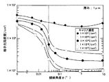
図4は、バッファ層2のSiドープのキャリア濃度を1×10²¹/cm3、1×1020/cm3、1×1019/cm3、1×1018/cm3、1×1017/cm3と変えた場合における、傾斜角度θとp−コンタクト層6表面の格子欠陥密度を前述と同様に測定して、その結果を示した図である。
【0035】
この図4から判るように、バッファ層2のキャリア濃度が1×10¹⁷/cm3〜1×1021/cm3の何れの場合においても、基板上面がC面から傾斜すると、p−コンタクト層6表面の格子欠陥密度は低下する。特に、バッファ層2のキャリア濃度が1×1020/cm3以下になると、格子欠陥密度の低下は大きく、その効果は傾斜角度θが0.03°以上で急激に現れる。更に、傾斜角度θが0.05°以上になると、バッファ層2のキャリア濃度に応じて格子欠陥密度が十分に低い値となる。
【0036】
また、バッファ層2のキャリア濃度が1×10¹⁸/cm3以下になると、上述した効果は一層顕著に現れる。特に、バッファ層2のキャリア濃度が1×1018/cm3以下の場合、傾斜角度θが1°まで大きくなると、格子欠陥密度が1×105/cm2程度に十分に小さくなり、傾斜角度θがそれ以上に大きくなっても、格子欠陥密度の更なる低下は表われなかった。
【0037】
本発明は、例えば、図5に示すようなリッジ導波型の半導体レーザ素子に用いることが可能である。
【0038】
図5において、11はGaNよりなる基板であり、基板11上にn−GaNからなるバッファ層12が形成され、その上にはn−InGaNからなるクラック防止層13、n−AlGaNからなる厚さ第1クラッド層14、アンドープのi−InGaNからなる多重量子井戸構造の活性層15、p−AlGaNからなる第2クラッド層16、p−GaNからなるp−コンタクト層17をMOCVD法により順に形成されている。第2クラッド層16の所定の深さまで除去されてストライプ状のリッジ部18が形成されている。基板11の下面にはn−電極19が、p−コンタクト層17の上面にはp−電極20が形成されている。また、リッジ部18の側面から第2クラッド層16のエッチング除去された上面に亘って保護膜21が形成されている。
【0039】
この構成の半導体レーザにおいて、上述の図2〜図4の結果に基づいて、基板1の上面をC面から所定角度θ傾斜させ、バッファ層12の厚み及びキャリア濃度を設定することにより、格子欠陥を減少させ、寿命を長くすることが出来る。
【0040】
尚、上述の図2〜図4は、基板1の上面の傾斜方向を<11−20>方向とした場合であるが、例えば<10−10>方向、<10−10>方向と<11−20>方向との間の方向等、他の方向に傾斜させた場合においても、略同様の結果が得られた。
【0041】
また、本発明は、セルフアライン構造等の他の半導体レーザは勿論のこと、半導体レーザ以外の他の半導体発光素子にも適用可能である。
【0042】
また、基板上に形成される窒化物系半導体層としても、上述した以外のものでも良く、III属元素として、Ga、或いはGaにAl、In、Bの少なくと1つを含んでいれば良い。またV族元素としてN以外にPやAs等を少量含んでいても良い。
【0043】
【発明の効果】
本発明に依れば、GaN基板の上に形成される窒化物系半導体層の結晶性が良く、長寿命化に適した窒化物系半導体発光素子を製造できる窒化物系半導体発光素子の製造方法を提供し得る。
【図面の簡単な説明】
【図1】本発明を用いた発光ダイオードの構成を示す断面図である。
【図2】発光ダイオードのコンタクト層表面の格子欠陥密度及び寿命と基板上面の傾斜角度との関係を示す図である。
【図3】発光ダイオードのバッファ層の厚みによるコンタクト層表面の格子欠陥密度及と、基板上面の傾斜角度との関係を示す図である。
【図4】発光ダイオードのバッファ層のキャリア濃度によるコンタクト層表面の格子欠陥密度及と、基板上面の傾斜角度との関係を示す図である。
【図5】本発明を用いたリッジ導波型半導体レーザ素子の構成を示す断面図である。
【符号の説明】
1、11 基板
2、12 バッファ層
3、14 n−クラッド層
4、15 活性層
5、16 pクラッド層[0001]
BACKGROUND OF THE INVENTION
The present invention relates to a method of manufacturing a nitride semiconductor light emitting device such as a semiconductor laser or a light emitting diode made of a nitride semiconductor material such as GaN.
[0002]
[Prior art]
Conventionally, in this type of nitride-based semiconductor light emitting device, a sapphire substrate is used as the substrate. However, since the sapphire substrate has a large lattice mismatch with the nitride-based semiconductor layer to be formed, the first buffer layer is formed on the sapphire substrate at a low temperature of 500 to 600 ° C., and then 900 to 1200. It was necessary to grow the second buffer layer at a high temperature of 0 ° C. and to form a nitride-based semiconductor layer such as a light emitting layer thereon.
[0003]
For this reason, recently, a method of forming a buffer layer directly on a GaN substrate at a high temperature of 900 to 1200 ° C. and forming a light emitting layer such as a cladding layer and an active layer thereon has been studied and proposed.
[0004]
However, simply forming a buffer layer on a GaN substrate at a high temperature does not satisfy the crystallinity of the light emitting layer formed thereon, and the light emitting characteristics deteriorate when the light emitting element is used for a long time. There's a problem.
[0005]
[Problems to be solved by the invention]
The present invention has been made in view of the drawbacks of the above-described conventional examples. The crystallinity of the nitride-based light emitting layer formed on the GaN substrate is good, and the light emission characteristics deteriorate even when used for a long time. It is an object of the present invention to provide a method for manufacturing a suppressed nitride-based semiconductor light-emitting device.
[0007]
[Means for Solving the Problems]
In the method for manufacturing a nitride-based semiconductor light-emitting device of the present invention, the thickness of the nitride semiconductor formed on the upper surface of the GaN substrate inclined at an angle of 0.03 ° or more and 10 ° or less with respect to the C-plane is 0.00. By growing a buffer layer of 5 μm or more at a temperature of 900 ° C. or more and 1200 ° C. or less, growing a light emitting layer made of a nitride semiconductor on the buffer layer, and forming a p-contact layer on the light emitting layer, On the p-contact layer, the lattice defect density on the surface of the p-contact layer is 1.0 × 10 6 / cm 2 or less and the lattice defect density on the surface is 1.0 × 10 6 / cm 2 or less. And p-electrodes are formed .
[0008]
In the semiconductor light emitting device manufactured in this way, the lattice defect density on the surface of the p-contact layer formed on the top surface of the semiconductor light emitting device formed on the top surface of the substrate is 1.0 × 10 6 / cm 2 or less. Long life.
[0009]
In particular, if the inclination angle of the upper surface of the substrate is 0.03 ° or more and 10 ° or less, the above-described reduction of the lattice defects appears clearly, and adverse effects due to the step-like step caused by the inclination are suppressed. .
[0010]
Furthermore, if the inclination angle of the upper surface of the substrate is 0.05 ° or more, the above-described reduction of lattice defects appears remarkably.
[0012]
If the thickness of the buffer layer is 0.5 μm or more, the above-described reduction of lattice defects appears more remarkably.
[0013]
Particularly, when the thickness of the buffer layer is 1 μm or more, the above-described reduction of lattice defects appears more remarkably.
[0014]
In this case, if the inclination angle of the upper surface of the substrate is 0.5 ° or less, the above-described reduction of lattice defects can be sufficiently obtained.
[0015]
Further, when the carrier concentration of the buffer layer is 1 × 10 20 / cm 3 or less, the above-mentioned reduction of lattice defects appears more remarkably.
[0016]
In particular, when the carrier concentration of the buffer layer is 1 × 10 18 / cm 3 or less, the above-described reduction of lattice defects appears more remarkably.
[0017]
In this case, if the inclination angle of the upper surface of the substrate is 1 ° or less, the above-described reduction of lattice defects can be sufficiently obtained.
[0021]
DETAILED DESCRIPTION OF THE INVENTION
Hereinafter, embodiments of the present invention will be described in detail with reference to the drawings.
[0022]
First, as shown in FIG. 1, a
A 0.8 μm thick n-cladding layer 3 made of Si-doped n-Al 0.1 Ga 0.9 N, an
[0023]
The
[0024]
The
[0025]
In addition, as a method for inclining the upper surface of the
[0026]
FIG. 2 is a diagram showing the relationship between the lattice defect density on the surface of the p-contact layer 6 and the lifetime when the tilt angle θ is changed in the light emitting diode having the configuration shown in FIG.
[0027]
The lattice defect density on the surface of the buffer layer 6 was determined by placing the light emitting diode in a NaOH or KOH solution and boiling at 400 ° C., and counting the number of defects per 1 cm 2 with an electron scanning line microscope. In addition, the lifetime is the time during which the emission intensity is reduced by 10% from the initial value when each sample is continuously operated by flowing a current of 30 mA in an environment of 70 ° C.
[0028]
As can be seen from FIG. 2, the upper surface of the substrate made of GaN is inclined from the C plane, and the light emitting element formed on the inclined upper surface is a light emitting element formed on the C plane (inclination angle θ = 0 °). In comparison with this, the lattice defect density on the surface of the p-contact layer 6 is lowered, and the lifetime is increased. The decrease in the lattice defect density on the surface of the p-contact layer 6 is due to the improved crystallinity of the
[0029]
In particular, when the tilt angle is 0.03 ° or more, the lattice defect density on the surface of the p-contact layer 6 is rapidly reduced to 1.0 × 10 6 / cm 2 or less, and the lifetime is significantly increased accordingly. I understand that.
[0030]
When a nitride layer is grown on a surface inclined from the C-plane of the
[0031]
FIG. 3 shows the measurement of the inclination angle θ and the lattice defect density on the surface of the p-contact layer 6 in the same manner as described above when the thickness of the
[0032]
As can be seen from FIG. 3, the
[0033]
Further, when the thickness of the
[0034]
FIG. 4 shows that the Si-doped carrier concentration of the
[0035]
As can be seen from FIG. 4, in any case where the carrier concentration of the
[0036]
Further, when the carrier concentration of the
[0037]
The present invention can be used, for example, in a ridge waveguide type semiconductor laser device as shown in FIG.
[0038]
In FIG. 5, 11 is a substrate made of GaN, a
[0039]
In the semiconductor laser having this configuration, lattice defects are obtained by inclining the upper surface of the
[0040]
2 to 4 described above are cases in which the inclination direction of the upper surface of the
[0041]
The present invention is applicable not only to other semiconductor lasers such as a self-aligned structure but also to other semiconductor light emitting elements other than the semiconductor laser.
[0042]
Further, the nitride-based semiconductor layer formed on the substrate may be other than those described above, and it is sufficient that Ga or Ga contains at least one of Al, In, and B as a group III element. . In addition to N, the group V element may contain a small amount of P, As, or the like.
[0043]
【The invention's effect】
INDUSTRIAL APPLICABILITY According to the present invention, a nitride-based semiconductor light- emitting device manufacturing method capable of manufacturing a nitride-based semiconductor light-emitting device having a good crystallinity of a nitride-based semiconductor layer formed on a GaN substrate and suitable for extending the lifetime Can provide.
[Brief description of the drawings]
FIG. 1 is a cross-sectional view showing a configuration of a light-emitting diode using the present invention.
FIG. 2 is a graph showing the relationship between the lattice defect density and lifetime on the contact layer surface of the light emitting diode and the tilt angle of the substrate upper surface.
FIG. 3 is a diagram showing the relationship between the lattice defect density on the surface of the contact layer and the inclination angle of the upper surface of the substrate depending on the thickness of the buffer layer of the light emitting diode.
FIG. 4 is a diagram showing the relationship between the lattice defect density on the surface of the contact layer due to the carrier concentration of the buffer layer of the light emitting diode and the inclination angle of the upper surface of the substrate.
FIG. 5 is a cross-sectional view showing a configuration of a ridge waveguide type semiconductor laser device using the present invention.
[Explanation of symbols]
1, 11
Claims (7)
Priority Applications (1)
| Application Number | Priority Date | Filing Date | Title |
|---|---|---|---|
| JP2218199A JP3668031B2 (en) | 1999-01-29 | 1999-01-29 | Method for manufacturing nitride-based semiconductor light-emitting device |
Applications Claiming Priority (1)
| Application Number | Priority Date | Filing Date | Title |
|---|---|---|---|
| JP2218199A JP3668031B2 (en) | 1999-01-29 | 1999-01-29 | Method for manufacturing nitride-based semiconductor light-emitting device |
Publications (2)
| Publication Number | Publication Date |
|---|---|
| JP2000223743A JP2000223743A (en) | 2000-08-11 |
| JP3668031B2 true JP3668031B2 (en) | 2005-07-06 |
Family
ID=12075636
Family Applications (1)
| Application Number | Title | Priority Date | Filing Date |
|---|---|---|---|
| JP2218199A Expired - Lifetime JP3668031B2 (en) | 1999-01-29 | 1999-01-29 | Method for manufacturing nitride-based semiconductor light-emitting device |
Country Status (1)
| Country | Link |
|---|---|
| JP (1) | JP3668031B2 (en) |
Cited By (1)
| Publication number | Priority date | Publication date | Assignee | Title |
|---|---|---|---|---|
| WO2023287874A1 (en) * | 2021-07-13 | 2023-01-19 | The Regents Of The University Of California | Fabrication method for small size light emitting diodes on high-quality epitaxial crystal layers |
Families Citing this family (45)
| Publication number | Priority date | Publication date | Assignee | Title |
|---|---|---|---|---|
| JP2000252591A (en) * | 1999-02-26 | 2000-09-14 | Sanyo Electric Co Ltd | Nitride system semiconductor element and its manufacturing method |
| JP3929008B2 (en) | 2000-01-14 | 2007-06-13 | シャープ株式会社 | Nitride-based compound semiconductor light-emitting device and method for manufacturing the same |
| US6596079B1 (en) | 2000-03-13 | 2003-07-22 | Advanced Technology Materials, Inc. | III-V nitride substrate boule and method of making and using the same |
| JP3696182B2 (en) * | 2001-06-06 | 2005-09-14 | 松下電器産業株式会社 | Semiconductor laser element |
| US7462882B2 (en) | 2003-04-24 | 2008-12-09 | Sharp Kabushiki Kaisha | Nitride semiconductor light-emitting device, method of fabricating it, and semiconductor optical apparatus |
| JP3841092B2 (en) | 2003-08-26 | 2006-11-01 | 住友電気工業株式会社 | Light emitting device |
| US7118813B2 (en) * | 2003-11-14 | 2006-10-10 | Cree, Inc. | Vicinal gallium nitride substrate for high quality homoepitaxy |
| JP2005191530A (en) | 2003-12-03 | 2005-07-14 | Sumitomo Electric Ind Ltd | Light emitting device |
| ATE418806T1 (en) | 2004-04-02 | 2009-01-15 | Nichia Corp | NITRIDE SEMICONDUCTOR LASER DEVICE |
| JP2005340765A (en) * | 2004-04-30 | 2005-12-08 | Sumitomo Electric Ind Ltd | Semiconductor light emitting device |
| CN100413102C (en) * | 2004-04-30 | 2008-08-20 | 住友电气工业株式会社 | semiconductor light emitting device |
| JP4581490B2 (en) * | 2004-05-31 | 2010-11-17 | 日立電線株式会社 | III-V group nitride semiconductor free-standing substrate manufacturing method and III-V group nitride semiconductor manufacturing method |
| JP4691911B2 (en) * | 2004-06-11 | 2011-06-01 | 日立電線株式会社 | III-V nitride semiconductor free-standing substrate manufacturing method |
| US7339255B2 (en) * | 2004-08-24 | 2008-03-04 | Kabushiki Kaisha Toshiba | Semiconductor device having bidirectionally inclined toward <1-100> and <11-20> relative to {0001} crystal planes |
| JP4693547B2 (en) * | 2004-08-24 | 2011-06-01 | 株式会社東芝 | Semiconductor substrate, semiconductor element, and semiconductor light emitting element |
| JP3816942B2 (en) | 2004-10-27 | 2006-08-30 | 三菱電機株式会社 | Manufacturing method of semiconductor device |
| US8368183B2 (en) | 2004-11-02 | 2013-02-05 | Sharp Kabushiki Kaisha | Nitride semiconductor device |
| JP4772314B2 (en) * | 2004-11-02 | 2011-09-14 | シャープ株式会社 | Nitride semiconductor device |
| JP4997744B2 (en) * | 2004-12-24 | 2012-08-08 | 日亜化学工業株式会社 | Nitride semiconductor device and manufacturing method thereof |
| JP2006210795A (en) * | 2005-01-31 | 2006-08-10 | Sanyo Electric Co Ltd | Compound semiconductor light emitting device |
| EP1873880A4 (en) * | 2005-03-31 | 2010-10-27 | Sanyo Electric Co | METHOD FOR MANUFACTURING GALLIUM NITRIDE COMPOUND SEMICONDUCTOR LASER ELEMENT AND COMPOUND-BASED SEMICONDUCTOR LASER ELEMENT BASED ON GALLIUM NITRIDE |
| KR100707187B1 (en) * | 2005-04-21 | 2007-04-13 | 삼성전자주식회사 | Gallium Nitride Compound Semiconductor Device |
| DE102005021099A1 (en) | 2005-05-06 | 2006-12-07 | Universität Ulm | GaN layers |
| JP5023318B2 (en) | 2005-05-19 | 2012-09-12 | 国立大学法人三重大学 | 3-5 nitride semiconductor multilayer substrate, 3-5 nitride semiconductor free-standing substrate manufacturing method, and semiconductor device |
| JP4857616B2 (en) * | 2005-06-17 | 2012-01-18 | ソニー株式会社 | Method for forming GaN-based compound semiconductor layer and method for manufacturing GaN-based semiconductor light-emitting device |
| WO2007008394A1 (en) * | 2005-07-11 | 2007-01-18 | Cree, Inc. | Laser diode orientation on mis-cut substrates |
| JP2007081182A (en) * | 2005-09-15 | 2007-03-29 | Matsushita Electric Ind Co Ltd | Semiconductor light emitting device |
| US7863623B2 (en) | 2005-09-15 | 2011-01-04 | Panasonic Corporation | Semiconductor light emitting device |
| JP2007081183A (en) * | 2005-09-15 | 2007-03-29 | Matsushita Electric Ind Co Ltd | Semiconductor light emitting device |
| JP2007081181A (en) * | 2005-09-15 | 2007-03-29 | Matsushita Electric Ind Co Ltd | Semiconductor light emitting device |
| US8691674B2 (en) | 2005-09-29 | 2014-04-08 | Sumitomo Chemical Company, Limited | Method for producing group 3-5 nitride semiconductor and method for producing light-emitting device |
| JP2007119325A (en) * | 2005-10-31 | 2007-05-17 | Sumitomo Electric Ind Ltd | Group III nitride crystal and growth method thereof |
| JP2006229253A (en) * | 2006-05-19 | 2006-08-31 | Sharp Corp | Nitride-based compound semiconductor light emission and method for manufacturing the same |
| US7755103B2 (en) | 2006-08-03 | 2010-07-13 | Sumitomo Electric Industries, Ltd. | Nitride gallium semiconductor substrate and nitride semiconductor epitaxial substrate |
| JP5032171B2 (en) * | 2007-03-26 | 2012-09-26 | 株式会社東芝 | Semiconductor light emitting device, method for manufacturing the same, and light emitting device |
| WO2009021201A1 (en) * | 2007-08-08 | 2009-02-12 | The Regents Of The University Of California | Planar nonpolar m-plane group iii-nitride films grown on miscut substrates |
| JP2009051686A (en) * | 2007-08-24 | 2009-03-12 | Sumitomo Electric Ind Ltd | Group III nitride crystal growth method |
| JP2009057247A (en) * | 2007-08-31 | 2009-03-19 | Sumitomo Electric Ind Ltd | Group III nitride crystal growth method and group III nitride crystal substrate |
| JP4924498B2 (en) * | 2008-03-18 | 2012-04-25 | 住友電気工業株式会社 | Nitride-based semiconductor light-emitting device, epitaxial wafer, and method for manufacturing nitride-based semiconductor light-emitting device |
| JP2009117875A (en) * | 2009-02-23 | 2009-05-28 | Sharp Corp | Manufacturing method of nitride semiconductor light emitting device |
| US9236530B2 (en) | 2011-04-01 | 2016-01-12 | Soraa, Inc. | Miscut bulk substrates |
| US9646827B1 (en) | 2011-08-23 | 2017-05-09 | Soraa, Inc. | Method for smoothing surface of a substrate containing gallium and nitrogen |
| JP2011254113A (en) * | 2011-09-16 | 2011-12-15 | Sumitomo Electric Ind Ltd | Method of manufacturing gallium nitride-based semiconductor laser |
| TW201511327A (en) | 2013-09-06 | 2015-03-16 | Ind Tech Res Inst | Light-emitting diode |
| WO2022181322A1 (en) * | 2021-02-25 | 2022-09-01 | 日本碍子株式会社 | Group-iii element nitride semiconductor substrate |
-
1999
- 1999-01-29 JP JP2218199A patent/JP3668031B2/en not_active Expired - Lifetime
Cited By (1)
| Publication number | Priority date | Publication date | Assignee | Title |
|---|---|---|---|---|
| WO2023287874A1 (en) * | 2021-07-13 | 2023-01-19 | The Regents Of The University Of California | Fabrication method for small size light emitting diodes on high-quality epitaxial crystal layers |
Also Published As
| Publication number | Publication date |
|---|---|
| JP2000223743A (en) | 2000-08-11 |
Similar Documents
| Publication | Publication Date | Title |
|---|---|---|
| JP3668031B2 (en) | Method for manufacturing nitride-based semiconductor light-emitting device | |
| JP3594826B2 (en) | Nitride semiconductor light emitting device and method of manufacturing the same | |
| US7053420B2 (en) | GaN group semiconductor light-emitting element with concave and convex structures on the substrate and a production method thereof | |
| US7083996B2 (en) | Nitride semiconductor device and manufacturing method thereof | |
| JP4169821B2 (en) | Light emitting diode | |
| EP1496584B1 (en) | Nitride semiconductor laser device and method of manufacturing the nitride semiconductor laser device | |
| JP2002016312A (en) | Nitride based semiconductor device and method of manufacturing | |
| JP2002016000A (en) | Nitride semiconductor element and nitride semiconductor substrate | |
| JP5076656B2 (en) | Nitride semiconductor laser device | |
| JP2002270971A (en) | Nitride semiconductor device | |
| JP4991025B2 (en) | Nitride semiconductor laser device | |
| JP4423969B2 (en) | Nitride semiconductor multilayer substrate and nitride semiconductor device and nitride semiconductor laser device using the same | |
| JP2008028375A (en) | Nitride semiconductor laser device | |
| JP2002280609A (en) | Ultraviolet light emitting element | |
| JP5532082B2 (en) | Nitride semiconductor laser device | |
| JP4104234B2 (en) | Semiconductor light emitting device and manufacturing method thereof | |
| JP4045792B2 (en) | Nitride semiconductor laser device | |
| JP2005101536A (en) | Nitride semiconductor laser device | |
| JP2003142769A (en) | Nitride semiconductor laser device | |
| JP3800146B2 (en) | Method of manufacturing nitride semiconductor device | |
| JP3439161B2 (en) | Nitride light emitting device | |
| JPH11274556A (en) | Semiconductor light emitting device and method of manufacturing the same | |
| JP5023567B2 (en) | Nitride semiconductor laser device | |
| WO2002069466A1 (en) | Iii group nitride semiconductor element and iii group nitride semiconductor substrate | |
| JP4868888B2 (en) | Method for manufacturing optical semiconductor element |
Legal Events
| Date | Code | Title | Description |
|---|---|---|---|
| A02 | Decision of refusal |
Free format text: JAPANESE INTERMEDIATE CODE: A02 Effective date: 20040921 |
|
| A521 | Request for written amendment filed |
Free format text: JAPANESE INTERMEDIATE CODE: A523 Effective date: 20041118 |
|
| A521 | Request for written amendment filed |
Free format text: JAPANESE INTERMEDIATE CODE: A523 Effective date: 20041228 |
|
| A911 | Transfer to examiner for re-examination before appeal (zenchi) |
Free format text: JAPANESE INTERMEDIATE CODE: A911 Effective date: 20050106 |
|
| TRDD | Decision of grant or rejection written | ||
| A01 | Written decision to grant a patent or to grant a registration (utility model) |
Free format text: JAPANESE INTERMEDIATE CODE: A01 Effective date: 20050315 |
|
| A61 | First payment of annual fees (during grant procedure) |
Free format text: JAPANESE INTERMEDIATE CODE: A61 Effective date: 20050407 |
|
| FPAY | Renewal fee payment (event date is renewal date of database) |
Free format text: PAYMENT UNTIL: 20090415 Year of fee payment: 4 |
|
| FPAY | Renewal fee payment (event date is renewal date of database) |
Free format text: PAYMENT UNTIL: 20100415 Year of fee payment: 5 |
|
| FPAY | Renewal fee payment (event date is renewal date of database) |
Free format text: PAYMENT UNTIL: 20110415 Year of fee payment: 6 |
|
| FPAY | Renewal fee payment (event date is renewal date of database) |
Free format text: PAYMENT UNTIL: 20120415 Year of fee payment: 7 |
|
| FPAY | Renewal fee payment (event date is renewal date of database) |
Free format text: PAYMENT UNTIL: 20130415 Year of fee payment: 8 |
|
| FPAY | Renewal fee payment (event date is renewal date of database) |
Free format text: PAYMENT UNTIL: 20140415 Year of fee payment: 9 |
|
| EXPY | Cancellation because of completion of term |