JP3668246B2 - Field emission cold cathode and manufacturing method thereof - Google Patents
Field emission cold cathode and manufacturing method thereof Download PDFInfo
- Publication number
- JP3668246B2 JP3668246B2 JP2004123179A JP2004123179A JP3668246B2 JP 3668246 B2 JP3668246 B2 JP 3668246B2 JP 2004123179 A JP2004123179 A JP 2004123179A JP 2004123179 A JP2004123179 A JP 2004123179A JP 3668246 B2 JP3668246 B2 JP 3668246B2
- Authority
- JP
- Japan
- Prior art keywords
- layer
- emitter
- structural
- gate electrode
- electrodes
- Prior art date
- Legal status (The legal status is an assumption and is not a legal conclusion. Google has not performed a legal analysis and makes no representation as to the accuracy of the status listed.)
- Expired - Fee Related
Links
Images







Landscapes
- Cold Cathode And The Manufacture (AREA)
Description
本発明は、電界放出型冷陰極及びその製造方法に関する。 The present invention relates to a field emission cold cathode and a manufacturing method thereof.
近年、Si半導体加工技術を利用した電界放出型冷陰極の開発が、活発に行なわれている。 In recent years, field emission cold cathodes using Si semiconductor processing technology have been actively developed.
電界放出型冷陰極は、カソード電極上に形成された円錐状或いはピラミッド状のエミッタと、エミッタ電極層の先端部から電子を引き出すためのゲート電極とから形成される。 The field emission cold cathode is formed of a conical or pyramidal emitter formed on the cathode electrode and a gate electrode for extracting electrons from the tip of the emitter electrode layer.
電界放出型冷陰極の形成方法には、大別するとSpindt法と転写モールド法との二つある。Spindt法で形成した場合、円錐状のエミッタを囲むように形成された絶縁層上にゲート電極が形成される。また、転写モールド法で形成した場合、エミッタの側面上に形成された絶縁膜を介してゲート電極が形成される。 There are roughly two methods of forming a field emission type cold cathode: Spindt method and transfer mold method. When formed by the Spindt method, a gate electrode is formed on an insulating layer formed so as to surround a conical emitter. When formed by the transfer mold method, a gate electrode is formed through an insulating film formed on the side surface of the emitter.
円錐状のエミッタから電子を引き出すために、ゲート電極とエミッタの間に電圧差を与えると、形状不均一性等のために異常放電が発生したり、ゲート電極とエミッタとの間に電界誘起応力が働き、ゲート電極とエミッタとが電気的に接触して短絡し、エミッタから電子が放出されないことがあるという問題があった。 If a voltage difference is applied between the gate electrode and the emitter in order to extract electrons from the conical emitter, abnormal discharge may occur due to non-uniform shape, etc., or an electric field induced stress between the gate electrode and the emitter. There is a problem in that the gate electrode and the emitter are electrically contacted and short-circuited, and electrons may not be emitted from the emitter.
また、電界放出型冷陰極が行方向及び列方向に2次元配列された小型のFEA(Field Emission Array)を基板上にタイリングして形成する技術が報告されている。ところが、小型のFEAに形成されたゲート電極を電気的に接続することが困難であるという問題があった。 In addition, a technique for forming a small field emission array (FEA) in which field emission cold cathodes are two-dimensionally arranged in a row direction and a column direction by tiling on a substrate has been reported. However, there is a problem that it is difficult to electrically connect the gate electrodes formed on the small FEA.
隣接するゲート電極をワイヤーボンディングを用いて電気的に接続し、大面積のFEAを形成する技術が報告されている。だが、ワイヤーボンディングを用いると製造コストが高いという問題点があった。 A technique has been reported in which adjacent gate electrodes are electrically connected using wire bonding to form a large area FEA. However, when wire bonding is used, the manufacturing cost is high.
上述したように、従来の電界放出型冷陰極には、電界誘起応力によってゲート電極とエミッタとが接触し短絡し、エミッタから電子が放出されないことがあるという問題があった。 As described above, the conventional field emission cold cathode has a problem that the gate electrode and the emitter are brought into contact with each other due to electric field induced stress and short-circuited, and electrons are not emitted from the emitter.
また、従来、大面積のFEAを安価に製造することができないという問題点があった。 Further, conventionally, there has been a problem that a large area FEA cannot be manufactured at low cost.
本発明の目的は、ゲート電極とエミッタとの短絡を防止して、信頼性の向上を図り得ると共に、大面積のFEAを容易に、且つ安価に製造することが可能となる電界放出型冷陰極及びその製造方法を提供することにある。 An object of the present invention is to prevent a short circuit between a gate electrode and an emitter, improve reliability, and make it possible to easily and inexpensively manufacture a large area FEA. And a manufacturing method thereof.
[構成]
本発明は、上記目的を達成するために以下のように構成されている。
[Constitution]
The present invention is configured as follows to achieve the above object.
本発明の一例に係わる電界放出型冷陰極は、絶縁基板上に行方向に沿って複数本配列形成されたカソード電極と、これらのカソード電極の何れかに電気的に接続され,行方向及び列方向に2次元配置された複数個のエミッタ電極と、列方向に沿って複数本形成され、前記エミッタ電極から電子を引き出すゲート電極とを含む電界放出型冷陰極であって、前記エミッタ電極及びゲート電極は、構造基板上に密接して配列された複数の構造基体にそれぞれ形成され、列方向に隣接する構造基体に形成されたゲート電極は、膜状のゲート電極接続層によって電気的に接続され、隣接する構造基体の隙間に、該隙間の開口部を塞ぐ第1の分離絶縁体が形成されていることを特徴とする。 A field emission cold cathode according to an example of the present invention includes a plurality of cathode electrodes arrayed in the row direction on an insulating substrate, and electrically connected to any one of these cathode electrodes. A field emission type cold cathode comprising a plurality of emitter electrodes arranged two-dimensionally in the direction and a plurality of gate electrodes formed along the column direction and drawing electrons from the emitter electrodes, wherein the emitter electrode and the gate electrodes are respectively formed in a plurality of structural substrates that are closely arranged on the structure substrate, a gate electrode formed on the structure base adjacent in the column direction, are electrically connected by a film-like gate electrode connecting layer In the gap between adjacent structural bases, a first isolation insulator that closes the opening of the gap is formed .
上記電界放出型冷陰極の好ましい実施態様を以下に示す。 Preferred embodiments of the field emission cold cathode are shown below.
隣接する構造基体の接合部は、前記絶縁基板上に形成された第2の分離絶縁体上に形成されている。 Adjacent structural base joints are formed on a second isolation insulator formed on the insulating substrate.
本発明の一例に係わる電界放出型冷陰極の製造方法は、行方向及び列方向に2次元配列された複数個のエミッタ電極と、列方向に沿って配列形成され前記エミッタ電極から電子を引き出すゲート電極とが形成された構造基体を複数形成する工程と、それぞれの構造基体と絶縁基板上に行方向に沿って複数本形成されたカソード電極とを、前記エミッタ電極層が介在し、且つ隣接する構造基体が密着するように各構造基体を配列させて接着する工程と、配列された各構造体間の隙間の開口部を塞ぐ分離絶縁体を形成する工程と、列方向に隣接する構造基体のゲート電極を電気的に接続する膜状のゲート電極接続導電層を、前記構造基体及びゲート電極上に選択的に形成する工程とを含むことを特徴とする。 A method of manufacturing a field emission cold cathode according to an example of the present invention includes a plurality of emitter electrodes arranged two-dimensionally in a row direction and a column direction, and a gate that is formed along the column direction and draws electrons from the emitter electrode. A step of forming a plurality of structural bases on which electrodes are formed and a plurality of cathode electrodes formed in the row direction on the respective structural bases and insulating substrates are adjacent to each other with the emitter electrode layer interposed therebetween. Arranging and adhering the structural bases so that the structural bases are in close contact with each other, forming a separation insulator that closes the openings of the gaps between the arranged structural bodies, and the adjacent structural bases in the column direction And a step of selectively forming a film-like gate electrode connection conductive layer for electrically connecting the gate electrodes on the structural substrate and the gate electrode.
[作用]
本発明は、上記構成によって以下の作用・効果を有する。
[Action]
The present invention has the following operations and effects by the above configuration.
複数のエミッタが形成された複数の構造基体をタイルを貼るように、密着させて2次元配列し(タイリング)、ゲート電極又はカソード電極の形成を行うことによって、カソード電極又はゲート電極が寸断されて電気的接続が取れなくなるようなことはないので、大面積のFEAを容易に形成することができる。また、生産性の大幅な向上を図ることができる。 A plurality of structural substrates on which a plurality of emitters are formed are two-dimensionally arranged in a tactile manner so as to attach a tile (tiling), and the gate electrode or the cathode electrode is formed, whereby the cathode electrode or the gate electrode is cut off. Therefore, the FEA having a large area can be easily formed. In addition, the productivity can be greatly improved.
また、タイリングの際、先端が先鋭な凸部上に、絶縁層,エッチング停止層及びモールド基板が形成されているので、エミッタ先端部が保護され、各構造基体の取り扱いが容易である。 Further, since the insulating layer, the etching stopper layer, and the mold substrate are formed on the convex portion having a sharp tip at the time of tiling, the tip portion of the emitter is protected and each structural substrate can be easily handled.
基板上に複数の構造基体をタイリングし、ゲート電極、或いはカソード電極を形成することによって、電極を連続的に形成することが可能となり、隣接する構造基板の間で電極が切れることがなく、容易に大面積の電界放出型冷陰極を形成することができる。 By tiling a plurality of structural bases on a substrate and forming a gate electrode or a cathode electrode, it becomes possible to form electrodes continuously, and the electrodes do not break between adjacent structural substrates, A field emission type cold cathode having a large area can be easily formed.
本発明の実施の形態を以下に図面を参照して説明する。 Embodiments of the present invention will be described below with reference to the drawings.
[第1実施形態]
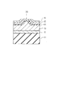
図1は、本発明の第1実施形態に係わる電界放出型冷陰極の構成を示す断面図である。
[First Embodiment]
FIG. 1 is a sectional view showing the structure of a field emission cold cathode according to the first embodiment of the present invention.
ガラス基板11上にITO電極層(カソード電極)12を介してエミッタ電極層13が形成されている。エミッタ電極層13の一部には、その平面に対してピラミッド状に突き出した凸部20が形成されている。エミッタ電極層13上にシリコン酸化膜14が形成されている。シリコン酸化膜14は、凸部20の先端部を除いて形成され、凸部20の先端が露出している。シリコン酸化膜14上に、シリコンにボロンがドープされた拡散層15(エッチング停止層)を介して、タングステン膜からなるゲート電極16が形成されている。
An
次に、図1に示した電解放出型冷陰極の製造工程を図2,3の斜視図を用いて説明する。 Next, the manufacturing process of the field emission cold cathode shown in FIG. 1 will be described with reference to the perspective views of FIGS.
先ず、図2(a)に示すように、p型の(001)シリコン単結晶基板(モールド基板)17の一方の表面に底部を尖らせた逆ピラミッド状の凹部18を形成する。シリコン単結晶基板に17に凹部18を形成する方法としては、シリコン単結晶基板の異方性エッチングを利用する方法がある。
First, as shown in FIG. 2A, an inverted pyramid-
すなわち、先ず、(100)結晶面方位のシリコン単結晶基板の表面に、厚さ0.1μmのシリコン酸化膜をドライ酸化法により形成し、更にレジストをスピンコート法により塗布する。次いで、レジストに例えば0.8μm□の開口部が得られるようにパターニングを行った後、レジストをマスクとしてNH4 F・HF混合溶液により、シリコン酸化膜を選択的にエッチングする。レジストを除去した後、シリコン酸化膜をマスクとして、30wt%のKOH水溶液を用いてシリコン単結晶基板に対して異方性エッチングを行うと、深さ0.56μmの逆ピラミッド状の凹部がシリコン単結晶基板に形成される。 That is, first, a silicon oxide film having a thickness of 0.1 μm is formed on the surface of a silicon single crystal substrate having a (100) crystal plane orientation by a dry oxidation method, and a resist is further applied by a spin coating method. Next, patterning is performed so that an opening of, for example, 0.8 μm □ is obtained in the resist, and then the silicon oxide film is selectively etched with an NH 4 F / HF mixed solution using the resist as a mask. After the resist is removed, anisotropic etching is performed on the silicon single crystal substrate using a 30 wt% aqueous KOH solution using the silicon oxide film as a mask, so that an inverted pyramid-shaped recess having a depth of 0.56 μm is formed on the silicon single crystal substrate. Formed on the crystal substrate.
次いで、シリコン単結晶基板17の表面に、熱拡散法を用いて3×1019cm-3以上の濃度になるようにボロンをドープし、エッチング停止層となる厚さ0.3μmの拡散層(剛体層)15を形成する。
Next, boron is doped on the surface of the silicon
次いで、図2(b)に示すように、拡散層15の表面に、ドライ酸化法を用いて厚さ0.2μm程度のシリコン酸化膜(絶縁層)14を形成する。なお、シリコン酸化膜14は、CVD法等によりシリコン酸化物を堆積することによっても形成することができる。
Next, as shown in FIG. 2B, a silicon oxide film (insulating layer) 14 having a thickness of about 0.2 μm is formed on the surface of the
熱酸化によって形成されたシリコン酸化膜は、緻密で厚さを制御することが容易であるので、熱酸化によってシリコン酸化膜を形成することが好ましい。シリコン酸化膜の膜厚を制御することによって、後に形成されるゲート電極とエミッタとの距離を精度良く調整することができる。 Since the silicon oxide film formed by thermal oxidation is dense and easy to control the thickness, it is preferable to form the silicon oxide film by thermal oxidation. By controlling the thickness of the silicon oxide film, the distance between the gate electrode and the emitter to be formed later can be adjusted with high accuracy.
また、熱酸化によってシリコン酸化膜14を形成した場合、シリコン酸化膜14の凹部18内部への成長作用によって、凹部18の底の先端部がシリコン酸化物を堆積によって形成した場合に比べて鋭くなり、後工程で形成されるエミッタの先がさらに鋭くなる。
Further, when the
次いで、図2(c)に示すように、シリコン酸化膜14上に、スパッタ法を用いてW膜を厚さ0.9μm堆積しエミッタ電極層13を形成する。なお、W以外にも、MoやTa等の材料をエミッタ電極層13として用いることが可能である。
Next, as shown in FIG. 2C, an
次いで、エミッタ電極層13上に、スパッタリング法を用いて、カソード電極となる厚さ1μm程度のITO電極層12を形成する。なお、エミッタ電極層13の材質によっては、ITO電極層12の形成を省くことができる。ITO電極層12を形成しなかった場合、エミッタ電極層13がカソード電極を兼ねることとなる。
Next, an
次いで、図2(d)に示すように、絶縁基板として、一方の面に厚さ0.4μmのAl層19が形成された厚さ1mmの石英ガラス基板11を用意し、ガラス基板11とITO電極層12とを接着する。この接着には、例えば、静電接着法を適用することが出来る。静電接着法は、冷陰極装置の軽量化や薄型化に寄与する。
Next, as shown in FIG. 2D, a 1 mm thick quartz glass substrate 11 having an
次いで、図2(e)に示すように、ガラス基板11の表面に形成されているAl層19を、HNO3 ・CH3 COOH・HFの混酸溶液を用いて選択的に除去した後、エチレンジアミン・ピロカテコール・ピラジンから成る水溶液(エチレンジアミン:75cc,ピロカテコール:12g,ピラジン:3mg,水:10cc)を用いてSi単結晶基板17を選択的にエッチング除去し、拡散層15を露出させる。この工程までで、エミッタ電極層13,シリコン酸化膜14及び拡散層15の一部が、拡散層15の平坦部に対してピラミッド状に突き出した凸部20が形成される。
Next, as shown in FIG. 2E, the
Si単結晶基板17をエッチングする際、厚さ0.3μmの拡散層15は、前述したエッチング溶液による浸食を終了させるエッチング停止層の役割を持つと同時に、先端が鋭く尖ったエミッタ電極層13の凸部20をエッチング溶液の侵食から保護する役目を果たす。従って、シリコン酸化膜14の膜厚が薄い場合でも、エミッタ電極層13をエッチング溶液の浸食から保護し、凸部20先端からの電界放出効率およびその均一性を大幅に向上させることができる。
When the Si
次いで、図3(f)に示すように、拡散層15上に、スパッタ法を用いてタングステン層を厚さ0.5μmとなるように堆積し、ゲート電極16を形成する。なお、駆動時の電流値にも依存するが、拡散層15のボロン濃度が、例えば1020〜1021cm-3と高く、抵抗率が10-4Ω・cmと低い場合には、拡散層15もゲート電極の役割を果たし、工程数及びコスト削減のみならず、ゲート−エミッタ間距離の近接化にも大きく寄与する。
Next, as shown in FIG. 3F, a tungsten layer is deposited on the
次いで、図3(g)に示すように、ゲート電極16上にスピンコート法を用いてフォトレジスト21を塗布し、ピラミッド状の凸部20先端部上に約0.9μm程度のフォトレジスト21が形成されているようにする。
Next, as shown in FIG. 3G, a
次いで、図3(h)に示すように、酸素プラズマによるドライエッチングによって、凸部20の先端部が0.7μmほど現れるように、レジスト層21の表面層をエッチング除去する。そして、反応性イオンエッチング法を用いて、凸部20の先端部のゲート電極16及び拡散層15をエッチングする。
Next, as shown in FIG. 3H, the surface layer of the resist
次いで、図3(i)に示すように、レジスト21を除去した後、NH4 F・HF混合溶液を用いて、シリコン酸化膜14を選択的に除去する。以上の工程までで、ゲート電極16に開口部が形成されるとともに、エミッタ電極層13の凸部20の先端部が露出し、ピラミッド状の冷陰極、すなわちエミッタが形成される。
Next, as shown in FIG. 3I, after the resist 21 is removed, the
なお、エミッタ電極層上にITO電極層を形成せずに、予め石英ガラス上に形成されたITO電極層とエミッタ電極層を接着して形成することも可能である。 It is also possible to form the ITO electrode layer formed on the quartz glass and the emitter electrode layer by bonding them without forming the ITO electrode layer on the emitter electrode layer.
本実施形態によれば、ゲート電極が剛体からなる拡散層から形成されていることによって、ゲート電極とエミッタ電極層の凸部とが短絡することがない。 According to this embodiment, since the gate electrode is formed of the diffusion layer made of a rigid body, the gate electrode and the convex portion of the emitter electrode layer are not short-circuited.
ゲート配線が、ゲート電極と拡散層の2層から形成され、その抵抗率が従来に比べて低くなっている。従って、大面積化した場合に信号遅延を抑制することができる。 The gate wiring is formed of two layers of a gate electrode and a diffusion layer, and its resistivity is lower than the conventional one. Therefore, signal delay can be suppressed when the area is increased.
[第2実施形態]
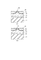
図4は、本発明の第2実施形態に係わる電界放出型冷陰極の構成を示す断面図である。図4において、図1と同一な部分には同一符号を付し、その説明を省略する。
[Second Embodiment]
FIG. 4 is a sectional view showing the structure of a field emission cold cathode according to the second embodiment of the present invention. 4, parts that are the same as those in FIG. 1 are given the same reference numerals, and explanation thereof is omitted.
本実施形態の特徴は、エミッタ電極層12のピラミッド状に形成された凸部20の先端付近まで、n型拡散層31が形成されており、拡散層31の表面がほぼ平坦になっていることである。
The feature of this embodiment is that the n-
本冷陰極は、第1実施形態の冷陰極に比べて拡散層31の膜厚が厚いうえ、さらにゲート配線の抵抗が減少し、大面積のFEAを形成しても信号遅延が起こりにくい。
In the present cold cathode, the
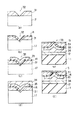
図5,6の工程断面図を用いて、図4に示した電界放出型冷陰極の製造工程を説明する。先ず、図5(a)に示すように、p型の(001)シリコン単結晶基板17の表面層に、熱拡散法或いはイオン注入法等を用いてn型拡散層31を形成する。
A manufacturing process of the field emission cold cathode shown in FIG. 4 will be described with reference to process cross-sectional views of FIGS. First, as shown in FIG. 5A, an n-
次いで、図5(b)に示すように、逆ピラミッド状の凹部32を、拡散層31及びシリコン基板17上に形成する。凹部32を形成する際、凹部32の開口部が拡散層31に形成され、凹部32の底の先端部がシリコン基板中17に形成されるようにする。シリコン基板17に凹部32を形成するには、第1実施形態において説明した方法を用いて形成することができる。
Next, as shown in FIG. 5B, an inverted pyramid-shaped
次いで、図5(c)に示すように、拡散層31及びシリコン基板17の表面に、ドライ酸化法を用いてシリコン酸化膜14を形成する。次いで、図7(d)に示すように、シリコン酸化膜14上にエミッタ電極層13及びカソード電極となるITO電極層12を順次積層する。エミッタ電極層13は、凹部内が埋め込まれるまで形成する。
Next, as shown in FIG. 5C, a
次いで、図5(e)に示すように、背面に厚さ0.4μmのAl層19が形成された厚さ1mmの石英ガラス基板11を用意し、ガラス基板11とシリコン単結晶基板17とをエミッタ電極層13が介するように接着する。この接着には、例えば、静電接着法を適用することが出来る。静電接着法は、冷陰極装置の軽量化や薄型化に寄与する。
Next, as shown in FIG. 5E, a quartz glass substrate 11 having a thickness of 1 mm with an
次いで、図5(f)に示すように、石英ガラス基板11背面のAl層19を除去した後、電気化学エッチング法を用いてシリコン単結晶基板17を選択的にエッチング除去し、拡散層31を露出させるとともに、拡散層31及びシリコン酸化膜14に覆われたエミッタ電極層13によるピラミッド形状の凸部33の先端部を露出させる。
Next, as shown in FIG. 5F, after the
電気化学エッチング法は、例えばKOH水溶液中で、n型拡散層31とp型のシリコン単結晶基板17との界面に生じているpn接合に対して逆電圧を印加してp型のシリコン単結晶基板を選択的にエッチングする方法である。
In the electrochemical etching method, for example, in a KOH aqueous solution, a p-type silicon single crystal is applied by applying a reverse voltage to a pn junction generated at the interface between the n-
次いで、図6(g)に示すように、拡散層31上に、電気メッキ法を用いて、ゲート電極16を形成する。電界メッキ法を用いてゲート電極16を形成すると、ゲート電極16は導電性を有する拡散層31の表面にのみ選択的に形成されるので、凸部33の先端部の絶縁性のシリコン酸化膜14上には形成されない。
Next, as shown in FIG. 6G, the
次いで、図6(h)に示すように、NH4 F・HF混合溶液を用いて、シリコン酸化膜14を選択的に除去する。この工程までで、ゲート電極16,拡散層31及びシリコン酸化膜14に開口部が形成されるとともに、エミッタ電極層13によるピラミッド状の凸部33の先端部が露出し、ピラミッド状の冷陰極、すなわちエミッタが形成される。
Next, as shown in FIG. 6H, the
なお、エミッタ電極層上にITO電極層を形成せずに、予め石英ガラス上に形成されたITO電極層とエミッタ電極層を接着して形成することも可能である。 It is also possible to form the ITO electrode layer formed on the quartz glass and the emitter electrode layer by bonding them without forming the ITO electrode layer on the emitter electrode layer.
[第3実施形態]
図7は、本発明の第3実施形態に係わる電界放出型冷陰極の構成を示す断面図である。なお、図1と同一な部分には同一符号を付し、その説明を省略する。
[Third Embodiment]
FIG. 7 is a sectional view showing the structure of a field emission cold cathode according to the third embodiment of the present invention. In addition, the same code | symbol is attached | subjected to the part same as FIG. 1, and the description is abbreviate | omitted.
本実施形態の特徴は、ITO電極層12とエミッタ電極層35との間に芯状抵抗層34が形成されていることである。エミッタ電極層35は、凸部33毎にそれぞれ分離されて形成されており、芯状抵抗層34によってITO電極層12と電気的に接続されている。
The feature of this embodiment is that a core-
製造時のバラツキでエミッタ電極層35の形状がそれぞれ異なる場合があるため、ゲート電極16との間隔が短いエミッタ電極層35から大量の電流が流れることによって、ゲート電極16とエミッタ電極層35との間に短絡が生じる可能性がある。しかし、芯状抵抗層34をエミッタ電極層35とITO電極層12との間に挿入することでITO電極層12からエミッタ電極層35に流れる電流を制限し、短絡を抑えることができる。
Since the shape of the
この図7に示した冷陰極の製造工程を図8の工程断面図を用いて説明する。図8(a),(b)は、第2実施形態の図5(a),(b)に示した工程と同様であるので、その説明を省略する。そして、図8(c)に示すように、シリコン酸化膜14上に電極材を堆積する。そして、凹部32を含む領域の電極材上にレジスト(不図示)を形成した後、レジストをマスクとしてRIE法を用いて電極材をエッチングしてエミッタ電極層35を形成し、レジストを除去する。
The manufacturing process of the cold cathode shown in FIG. 7 will be described with reference to the process cross-sectional view of FIG. 8A and 8B are the same as the steps shown in FIGS. 5A and 5B of the second embodiment, and a description thereof will be omitted. Then, an electrode material is deposited on the
次いで、図8(d)に示すように、シリコン酸化膜34及びエミッタ電極層35上に、芯状抵抗層34を堆積する。
Next, as shown in FIG. 8D, a
次いで、図8(e)に示すように、芯状抵抗層34上にITO電極層12を形成した後、第2実施形態と同様に、石英ガラス基板11とITO電極層12の接着,シリコン単結晶基板17の選択的除去及びゲート電極16の形成を順次行う。
Next, as shown in FIG. 8E, after the
そして、図8(f)に示すように、第2実施形態と同様に、拡散層31及びシリコン酸化膜14を選択的にエッチングすることによって、エミッタ電極層35が露出し、電界放出型冷陰極が完成する。
Then, as shown in FIG. 8 (f), as in the second embodiment, by selectively etching the
なお、芯状抵抗層上にITO電極層を形成せずに、予め石英ガラス上に形成されたITO電極層とエミッタ電極層を接着して形成することも可能である。 Instead of forming the ITO electrode layer on the core-like resistive layer, it is also possible to bond the ITO electrode layer formed on the quartz glass and the emitter electrode layer in advance.
[第4実施形態]
図9は、本発明の第4実施形態に係わるFEAの構成を示す断面図である。図9において、図7と同一な部分には同一符号を付し、その説明を省略する。
[Fourth Embodiment]
FIG. 9 is a cross-sectional view showing the configuration of the FEA according to the fourth embodiment of the present invention. 9, parts that are the same as those in FIG. 7 are given the same reference numerals, and explanation thereof is omitted.
本実施形態の特徴は、先端が先鋭な凸部を有するエミッタ電極層35が複数個配列形成された構造基体43a〜dが、石英ガラス基板41上に行方向に沿って形成されたカソード電極ライン42a,b上に、行方向及び列方向に密着して2次元配置されていることである。そして、構造基体43a〜d上に、ゲート電極44a,bが列方向に沿って配列形成されている。
A feature of this embodiment is that a
なお、図7は、構造基体43a〜dの接合部を拡大して図示した図であり、各構造基体43には、図示されている部分以外に多くのエミッタ電極層35が形成されている。また、カソード電極42とゲート電極44の交差部に一つの構造基体が配置されているように図示されているが、一つの構造基体にカソード電極42とゲート電極44の交差部が複数個形成されている。
FIG. 7 is an enlarged view of the joint portions of the
この冷陰極の製造工程を図10〜12の工程図を用いて説明する。 The manufacturing process of this cold cathode is demonstrated using process drawing of FIGS.
先ず、図10(a)に示すように、第3実施形態の図8(a)〜(d)に示した工程を用いて複数のエミッタ電極層35を形成した後、芯状抵抗層34の形成及びパターニングを行った構造基体43a〜dを用意する。また、表面にカソード電極42a,bが行方向に沿って形成された石英ガラス基板41を用意する。
First, as shown in FIG. 10A, after forming the plurality of emitter electrode layers 35 using the steps shown in FIGS. 8A to 8D of the third embodiment, the
次いで、図11(b)に示すように、構造基体43a〜dと石英ガラス基板41のカソード電極42a,bが形成されている面とを、エミッタ電極層35が介在するように接着する。つまり芯状抵抗層34とカソード電極42a,bとを接着する。
Next, as shown in FIG. 11B, the structure bases 43a to 43d and the surface on which the
次いで、図11(c)に示すように、第3実施形態と同様にシリコン単結晶基板11を選択的にエッチング除去し、拡散層35の凸部33を露出させる。
Next, as shown in FIG. 11C, the silicon single crystal substrate 11 is selectively removed by etching in the same manner as in the third embodiment, so that the
次いで、図12(d)に示すように、拡散層31上にスクリーン印刷方法を用いてゲート電極44a,bを列方向に沿って形成する。拡散層31の表面は、突起が一部にあるだけで、その表面は平坦であるため、容易にゲート電極44a,bをスクリーン印刷によって形成することができる。
Next, as shown in FIG. 12D,
このとき、隣接する構造基体43の間の隙間が大きいと、ゲート電極44が断切れを起こすおそれがある。そのため、隙間を埋め込むようにゲート電極44を形成すると、断切れを起こす事を防止することができる。また、隙間を埋め込むように形成した際、カソード電極42と絶縁されていれば、ゲート電極44がガラス基板上に形成されていても良い。また、ゲート電極44が形成される位置のガラス基板上に接続電極を形成しておき、ゲート電極が接続電極上に形成されるようにすると、更にゲート電極の電気的接続を確実にすることができる。
At this time, if the gap between adjacent
そして、図12(e)に示すように、ゲート電極44a,bをパターニングし、拡散層31を露出させた後、拡散層31及びシリコン酸化膜14を順次エッチングし、エミッタ電極層35の先端が先鋭な凸部を露出させる。以上説明した工程で本実施形態のFEAが形成される。
Then, as shown in FIG. 12E, after patterning the
本実施形態によれば、予め複数のエミッタが形成された構造基体を予めカソード電極が形成された石英ガラス基板上に配列した後、エミッタ上のシリコン単結晶基板を選択的に除去し、ゲート電極を形成することによって、ワイヤボンディングを用いることなく大面積のFEAを形成することができる。 According to this embodiment, after arranging the structure base on which the plurality of emitters are formed in advance on the quartz glass substrate on which the cathode electrode is formed in advance, the silicon single crystal substrate on the emitter is selectively removed, and the gate electrode By forming the FEA, a large area FEA can be formed without using wire bonding.
また、ゲート電極の形成に印刷法を用いることによって、簡易に列方向に沿ったゲート電極を形成することができる。 Further, by using a printing method for forming the gate electrode, it is possible to easily form the gate electrode along the column direction.
なお、構造基体43は、第1実施形態の図2(a)〜(c)に示した工程を経て形成された構造、又は第2実施形態の図5(a)〜(d)に示した工程を経て形成された構造を用いても良い。
In addition, the structure base |
[第5実施形態]
図13は、本発明の第5実施形態に係わるFEAの構成を示す断面図である。図13において、図9と同一な部分には同一符号を付し、その説明を省略する。
[Fifth Embodiment]
FIG. 13 is a cross-sectional view showing the configuration of the FEA according to the fifth embodiment of the present invention. In FIG. 13, the same parts as those in FIG.
本実施形態のFEAの特徴は、ゲート電極接続導電層51(51a,b)が、ゲート電極44(44a,b)上に形成されていることである。それぞれのゲート電極接続導電層51a,bは、隣接する構造基体43の接合部上に位置するゲート電極44上に選択的に形成されている。ゲート電極接続層51を形成することによって、隣接する構造基体43の間におけるゲート電極の電気的接続を確実に行うことができる。
The feature of the FEA of this embodiment is that the gate electrode connection conductive layer 51 (51a, b) is formed on the gate electrode 44 (44a, b). Each of the gate electrode connection conductive layers 51a and 51b is selectively formed on the gate electrode 44 located on the junction between adjacent
図13に示したFEAの製造工程を図14の工程図を用いて説明する。先ず、図14(a)に示すように、図10(a)〜図12(d)に示した工程を経て形成された構造に対して、隣接する構造基体43の接合部を含む領域のゲート電極44上に、スクリーン印刷法を用いてゲート電極接続導電層51a,bを形成する。なお、全面に電極材を堆積した後、パターニングしてゲート電極接続導電層51を形成することも可能である。
A manufacturing process of the FEA shown in FIG. 13 will be described with reference to the process diagram of FIG. First, as shown in FIG. 14A, the gate of the region including the joint portion of the
次いで、図14(b)に示すように、先の実施形態で説明した工程と同様に、ゲート電極44,拡散層31及びシリコン酸化膜14をエッチングすることによってエミッタ電極層35の凸部先端を露出させて、本実施形態のFEAが完成する。
Next, as shown in FIG. 14B, similarly to the process described in the previous embodiment, the gate electrode 44, the
なお、エミッタ電極層35の凸部先端を露出させた後、ゲート電極接続導電層を形成することも可能である。
It is also possible to form the gate electrode connection conductive layer after exposing the tip of the convex portion of the
[第6実施形態]
図15は、本発明の第6実施形態に係わるFEAの構成を示す断面図である。図15において、図9と同一な部分には同一符号を付し、その説明を省略する。
[Sixth Embodiment]
FIG. 15 is a cross-sectional view showing the configuration of the FEA according to the sixth embodiment of the present invention. In FIG. 15, the same parts as those of FIG.
本実施形態の特徴は、隣接する構造基体61a,bの隙間部62に、ガラス,SOG(Spin On Glass ),シリコン酸化物又はシリコン窒化物からなる絶縁層63が埋め込まれていることである。絶縁層63が隙間部62に埋め込まれていることによって、ゲート電極44a,bを堆積する際、構造基体の繋ぎ目の隙間部62において、ゲート電極44a,bがITO電極層44a上に形成されるのを防ぎ、ゲート電極44a,bとITO電極層42aとが短絡することを防ぐ。
The feature of this embodiment is that an insulating
図15に示したFEAの製造工程を図16,17の工程図を用いて説明する。 The manufacturing process of the FEA shown in FIG. 15 will be described with reference to the process diagrams of FIGS.
先ず、図16(a)に示した構造は、先に説明した図10(a)〜図11(c)に示した工程を経て形成されるものである。図示したように、構造基体61aと構造基体61bとの間に、隙間部62が生じている。
First, the structure shown in FIG. 16A is formed through the steps shown in FIGS. 10A to 11C described above. As illustrated, a
次いで、図16(b)に示すように、基板61a,b間の隙間部62を埋めるように、絶縁層63を形成する。
Next, as shown in FIG. 16B, an insulating
次いで、図17(c)に示すように、エッチバック法等を用いて、拡散層31上の絶縁層63を除去し、隙間部62に絶縁層63を埋め込み形成する。なお、隙間部62の全てを絶縁層63で埋め込む必要はなく、隙間部62の開口部を塞ぐように形成されていればよい。
Next, as shown in FIG. 17C, the insulating
次いで、図17(d)に示すように、第4実施形態と同様にゲート電極44a,bを形成した後、ゲート電極,拡散層31及びシリコン酸化膜14を選択的に除去することによってFEAが完成する。
Next, as shown in FIG. 17D, after the
なお、構造基体61は、第1実施形態の図2(a)〜(c)に示した工程を経て形成された構造、又は第2実施形態の図5(a)〜(d)に示した工程を経て形成された構造を用いても良い。 In addition, the structure base | substrate 61 was shown in the structure formed through the process shown to FIG. 2 (a)-(c) of 1st Embodiment, or FIG. 5 (a)-(d) of 2nd Embodiment. A structure formed through a process may be used.
[第7実施形態]
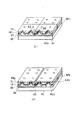
図18は、本発明の第7実施形態に係わるFEAの構成を示す斜視図である。図18において、図9と同一な部分には同一符号を付し、その説明を省略する。
[Seventh Embodiment]
FIG. 18 is a perspective view showing the configuration of the FEA according to the seventh embodiment of the present invention. In FIG. 18, the same parts as those in FIG. 9 are denoted by the same reference numerals, and the description thereof is omitted.
本実施形態のFEAの特徴は、隣接する構造基体43の接合部を含む領域の下に絶縁層71が形成されていることである。隣接する構造基体43の接合部の下に絶縁層が形成されていることによって、ゲート電極44とカソード電極42とが電気的に接続することを防止することができる。
A feature of the FEA of the present embodiment is that an insulating
図19,20の工程図を用いて、図18に示したFEAの製造工程を説明する。 The manufacturing process of the FEA shown in FIG. 18 will be described with reference to the process diagrams of FIGS.
先ず、図19(a)に示すように、図8(a)〜(d)に示した工程を経て形成された構造に対し、芯状抵抗層34がパターニングされた構造基体43a〜dを用意する。また、石英ガラス基板41上に、カソード電極ライン42a,b及び絶縁層71が形成された構造基板70を用意する。なお、絶縁層71は、後工程で構造基板70上に構造基体43をタイリングする際、隣接する基体43の接合部を含む領域に接する部位に形成されている。
First, as shown in FIG. 19A,
次いで、図20(b)に示すように、各構造基体43の抵抗層34が形成されている面と基板70のカソード電極42a,bが形成されている面とを接着する。このとき、絶縁層71上に、隣接する構造基体43の接合部が必ず存在するようにタイリングする。
Next, as shown in FIG. 20B, the surface of each
次いで、図20(c)に示すように、各シリコン単結晶基板17の除去、ゲート電極44a,bの形成、ゲート電極44,拡散層31及びシリコン酸化膜14のエッチングを順次行うことによって、本実施形態のFEAが完成する。
Next, as shown in FIG. 20C, the silicon
なお、構造基体43は、第1実施形態の図2(a)〜(c)に示した工程を経て形成された構造、又は第2実施形態の図5(a)〜(d)に示した工程を経て形成された構造を用いても良い。
In addition, the structure base |
[第8実施形態]
図21,22は、本発明の第8実施形態に係わる電界放出型冷陰極の製造工程を示す工程断面図である。
[Eighth Embodiment]
21 and 22 are process cross-sectional views illustrating the manufacturing process of the field emission cold cathode according to the eighth embodiment of the present invention.
先ず、図21(a)に示すように、支持基板81と、図8(a)〜(d)に示した工程を経て形成された構造に対し、芯状抵抗層34がパターニングされた構造基体82a〜dのシリコン基板17面とを仮接着する。
First, as shown in FIG. 21A, a structural substrate in which a core
次いで、図21(b)に示すように、芯状抵抗層34上にカソード電極83a,bをスクリーン印刷法を用いて行方向に沿って形成する。
Next, as shown in FIG. 21B,
次いで、図22(c)に示すように、カソード電極83a,bと石英ガラス基板84とを接着する。そして、支持基板81及びシリコン単結晶基板17を除去することによって、図11(c)に示した構造が形成される。後の工程は、図11(c)〜図12(e)に示した工程と同様の工程を行うことによって本実施形態のFEAが完成する。
Next, as shown in FIG. 22C, the
[第9実施形態]
図23は、本発明の第9実施形態に係わるFEAの構成を示す斜視図である。図23において、図9と同一な部分には同一符号を付し、その説明を省略する。
[Ninth Embodiment]
FIG. 23 is a perspective view showing the configuration of the FEA according to the ninth embodiment of the present invention. In FIG. 23, the same parts as those of FIG. 9 are denoted by the same reference numerals, and the description thereof is omitted.
本実施形態の特徴は、隣接する構造基体と接合部と接するカソード電極83の下部にカソード電極接続導電層92(92a,b)が形成されていることである。カソード電極接続導電層92を形成することによって、隣接する構造基体83間におけるカソード電極83の電気的接続を確実にすることができる。 A feature of this embodiment is that a cathode electrode connection conductive layer 92 (92a, 92b) is formed below the cathode electrode 83 in contact with the adjacent structural base and the joint. By forming the cathode electrode connection conductive layer 92, the electrical connection of the cathode electrode 83 between the adjacent structural bases 83 can be ensured.
図23に示したFEAの製造工程を図24の工程図を用いて説明する。 A manufacturing process of the FEA shown in FIG. 23 will be described with reference to the process diagram of FIG.
先ず、図21(a),(b)に示した工程を経て形成された構造を用意する。そして、表面にカソード電極接続電極層92a,bが形成されている石英ガラス基板91を用意する。石英ガラス基板91上のカソード電極接続導電層92は、隣接する構造基体の接合部とカソード電極83a,bとの交差部を含む領域に面するガラス基板91上に形成されている。
First, a structure formed through the steps shown in FIGS. 21A and 21B is prepared. Then, a
次いで、カソード電極接続導電層92とカソード電極83とを接着した後、支持基板81及びシリコン基板17を除去し、ゲート電極44の形成、拡散層31及びシリコン酸化膜14のエッチングを行うことによってFEAが完成する。
Next, after the cathode electrode connection conductive layer 92 and the cathode electrode 83 are bonded together, the
なお、本発明は、上記実施形態に限定されるものではない。例えば、上述したFEAを用いてFED(Field Emission Display)、或いは電子ビーム露光装置を形成することも可能である。 The present invention is not limited to the above embodiment. For example, an FED (Field Emission Display) or an electron beam exposure apparatus can be formed using the above-described FEA.
また、剛体層(エッチング停止層)は、シリコンに不純物がドープされた拡散層に限らず、ゲート電極より固く、電界誘起応力によって変位しないものであれば任意の材料を用いることができる。また、シリコン基板(モールド基板)上に剛体層を堆積して形成しても良い。 The rigid layer (etching stop layer) is not limited to a diffusion layer in which impurities are doped in silicon, and any material can be used as long as it is harder than the gate electrode and is not displaced by electric field induced stress. Further, a rigid layer may be deposited on a silicon substrate (mold substrate).
また、エミッタ電極層の材料としては、タングステンに限らず、仕事関数の低い種々の材料を用いることができる。 The material of the emitter electrode layer is not limited to tungsten, and various materials having a low work function can be used.
また、上記第4〜9実施形態に示した製造方法を適宜組み合わせてFEAを形成することも可能である。 Further, the FEA can be formed by appropriately combining the manufacturing methods shown in the fourth to ninth embodiments.
また、ゲート電極の形成に際し、蒸着法、或いはスパッタリング法等を用いることが可能である。 In forming the gate electrode, an evaporation method, a sputtering method, or the like can be used.
また、Spindt法等で形成された冷陰極が2次元配列され、且つゲート電極が列方向に沿って形成された複数の構造基体を密着配列した後、列方向に隣接する構造基体のゲート電極を膜状のゲート電極接続層で電気的に接続することも可能である。また、ゲート電極とカソード電極とが同一平面内に形成された平面型の冷陰極が形成された構造基体を同様にタイリングすることも可能である。 In addition, after the cold cathodes formed by the Spindt method or the like are two-dimensionally arranged and a plurality of structural bases in which the gate electrodes are formed in the column direction are closely arranged, the gate electrodes of the structural bases adjacent in the column direction are arranged. It is also possible to electrically connect with a film-like gate electrode connection layer. In addition, it is possible to similarly tile a structural substrate on which a planar cold cathode in which a gate electrode and a cathode electrode are formed in the same plane is formed.
ゲート電極接続層の形成の際、隣接する構造基体の接合部で上述した実施形態で説明したように断切れを起こす事がある。そのため、隙間を埋め込むようにゲート電極接続層を形成すると、断切れを起こす事を防止することができる。また、隙間を埋め込むように形成した際、カソード電極と絶縁されていれば、ゲート電極接続層が構造基板上に形成されていても良い。また、ゲート電極が形成される位置の構造基板上に接続電極を形成しておき、ゲート電極接続層が接続電極上に形成されるようにすると、更にゲート電極の電気的接続を確実にすることができる。 When the gate electrode connection layer is formed, breakage may occur at the junction between adjacent structural bases as described in the above-described embodiment. Therefore, when the gate electrode connection layer is formed so as to fill the gap, it is possible to prevent disconnection. Further, the gate electrode connection layer may be formed on the structure substrate as long as it is insulated from the cathode electrode when formed so as to fill the gap. Further, if the connection electrode is formed on the structure substrate at the position where the gate electrode is formed and the gate electrode connection layer is formed on the connection electrode, the electrical connection of the gate electrode is further ensured. Can do.
また、構造基体が配列形成された複数の構造基板を2次元配列して、更に大面積のFEAを形成することも可能である。この場合、構造基板にカソード電極に接続するスルーホールを設け、該スルーホールを用いて隣接する構造基板のカソード電極を電気的に接続することが可能である。 It is also possible to form a larger area FEA by two-dimensionally arranging a plurality of structural substrates on which structural bases are arranged. In this case, it is possible to provide a through hole connected to the cathode electrode in the structural substrate, and to electrically connect the cathode electrode of the adjacent structural substrate using the through hole.
その他、本発明は、その要旨を逸脱しない範囲で、種々変形して実施することが可能である。 In addition, the present invention can be variously modified and implemented without departing from the scope of the invention.
11…ガラス基板
12…ITO電極層(カソード電極)
13…エミッタ電極層
14…シリコン酸化膜
15…拡散層
16…ゲート電極
17…シリコン単結晶基板
18…凹部
19…Al層
20…凸部
21…レジスト
31…拡散層
32…凹部
33…凸部
34…芯状抵抗層
35…エミッタ電極層
41…石英ガラス基板
42a,b…カソード電極
43a〜d…構造基体
44a,b…ゲート電極
51a,b…ゲート電極接続導電層
61…構造基体
62…隙間部
63…絶縁層
71…絶縁分離層
81…支持基板
83a,b…カソード電極
91…石英ガラス基板
92a,b…カソード電極接続導電層
11 ...
DESCRIPTION OF
Claims (3)
前記エミッタ電極及びゲート電極は、構造基板上に密接して配列された複数の構造基体にそれぞれ形成され、
列方向に隣接する構造基体に形成されたゲート電極は、膜状のゲート電極接続層によって電気的に接続され、
隣接する構造基体の隙間に、該隙間の開口部を塞ぐ第1の分離絶縁体が形成されている
ことを特徴とする電界放出型冷陰極。 A plurality of cathode electrodes arrayed in the row direction on an insulating substrate; a plurality of emitter electrodes electrically connected to any one of these cathode electrodes and arranged two-dimensionally in the row direction and the column direction; A field emission type cold cathode comprising a plurality of gate electrodes formed along the column direction and including a gate electrode for extracting electrons from the emitter electrode;
The emitter electrode and the gate electrode are respectively formed on a plurality of structural bases arranged closely on a structural substrate,
The gate electrodes formed on the structural bases adjacent in the column direction are electrically connected by a film-like gate electrode connection layer ,
A field emission cold cathode characterized in that a first separation insulator for closing an opening of the gap is formed in a gap between adjacent structural substrates .
それぞれの構造基体と絶縁基板上に行方向に沿って複数本形成されたカソード電極とを、前記エミッタ電極層が介在し、且つ隣接する構造基体が密着するように各構造基体を配列させて接着する工程と、Each structural substrate and a plurality of cathode electrodes formed in the row direction on the insulating substrate are aligned and bonded so that the emitter electrode layer is interposed and adjacent structural substrates are in close contact with each other. And a process of
配列された各構造体間の隙間の開口部を塞ぐ分離絶縁体を形成する工程と、Forming a separation insulator that closes an opening of a gap between the arranged structures; and
列方向に隣接する構造基体のゲート電極を電気的に接続する膜状のゲート電極接続導電層を、前記構造基体及びゲート電極上に選択的に形成する工程とを含むことを特徴とする電界放出型冷陰極の製造方法。And a step of selectively forming a film-like gate electrode connection conductive layer electrically connecting the gate electrodes of the structural bases adjacent in the column direction on the structural base and the gate electrodes. Type cold cathode manufacturing method.
Priority Applications (1)
| Application Number | Priority Date | Filing Date | Title |
|---|---|---|---|
| JP2004123179A JP3668246B2 (en) | 2004-04-19 | 2004-04-19 | Field emission cold cathode and manufacturing method thereof |
Applications Claiming Priority (1)
| Application Number | Priority Date | Filing Date | Title |
|---|---|---|---|
| JP2004123179A JP3668246B2 (en) | 2004-04-19 | 2004-04-19 | Field emission cold cathode and manufacturing method thereof |
Related Parent Applications (1)
| Application Number | Title | Priority Date | Filing Date |
|---|---|---|---|
| JP869998A Division JP3559440B2 (en) | 1998-01-20 | 1998-01-20 | Field emission cold cathode and method of manufacturing the same |
Publications (2)
| Publication Number | Publication Date |
|---|---|
| JP2004214221A JP2004214221A (en) | 2004-07-29 |
| JP3668246B2 true JP3668246B2 (en) | 2005-07-06 |
Family
ID=32822442
Family Applications (1)
| Application Number | Title | Priority Date | Filing Date |
|---|---|---|---|
| JP2004123179A Expired - Fee Related JP3668246B2 (en) | 2004-04-19 | 2004-04-19 | Field emission cold cathode and manufacturing method thereof |
Country Status (1)
| Country | Link |
|---|---|
| JP (1) | JP3668246B2 (en) |
Families Citing this family (1)
| Publication number | Priority date | Publication date | Assignee | Title |
|---|---|---|---|---|
| KR101128303B1 (en) * | 2004-09-30 | 2012-03-23 | 가부시키가이샤 트리케미컬 겐큐쇼 | Film forming material, film forming method and device |
-
2004
- 2004-04-19 JP JP2004123179A patent/JP3668246B2/en not_active Expired - Fee Related
Also Published As
| Publication number | Publication date |
|---|---|
| JP2004214221A (en) | 2004-07-29 |
Similar Documents
| Publication | Publication Date | Title |
|---|---|---|
| JPH0782811B2 (en) | Field emitter structure and manufacturing method | |
| JPH0799666B2 (en) | Method and structure for manufacturing integrated vacuum microelectronic device | |
| US5965898A (en) | High aspect ratio gated emitter structure, and method of making | |
| KR100205051B1 (en) | Method for manufacturing field emission display device | |
| JP3249288B2 (en) | Micro vacuum tube and method of manufacturing the same | |
| JPH0982213A (en) | Field emission cold cathode device and manufacturing method thereof | |
| US5502314A (en) | Field-emission element having a cathode with a small radius | |
| US5585689A (en) | Field-emission cathode having integrated electrical interconnects and electron tube using the same | |
| JP2000500266A (en) | Field emitter device and bale process for fabricating the same | |
| US6626720B1 (en) | Method of manufacturing vacuum gap dielectric field emission triode and apparatus | |
| CN101013642A (en) | Method of manufacturing field emission device | |
| JP3195547B2 (en) | Vacuum sealed field emission type electron source device and manufacturing method thereof | |
| JP3559440B2 (en) | Field emission cold cathode and method of manufacturing the same | |
| KR19990024672A (en) | Method for manufacturing field emission array (FA) on silicon (SOI) substrate formed on insulating layer | |
| JPH06196086A (en) | Electric field emission negative electrode and its forming method | |
| JP2004214221A (en) | Field emission cold cathode and method of manufacturing the same | |
| JP2735009B2 (en) | Method for manufacturing field emission electron gun | |
| JP3529612B2 (en) | Field emission cold cathode and method of manufacturing the same | |
| JP2001035352A (en) | Electron source, method of manufacturing the same, and image forming apparatus formed using the same | |
| JPH09270228A (en) | Method of manufacturing field emission electron source | |
| US6572425B2 (en) | Methods for forming microtips in a field emission device | |
| JP3390255B2 (en) | Field emission cathode device and method of manufacturing the same | |
| JPH0574327A (en) | Electron-emitting device | |
| JPH03261040A (en) | Micro vacuum tube and its manufacture | |
| WO1999010911A1 (en) | Conductive address structure for field emission displays and method of manufacturing conductive structure |
Legal Events
| Date | Code | Title | Description |
|---|---|---|---|
| A977 | Report on retrieval |
Free format text: JAPANESE INTERMEDIATE CODE: A971007 Effective date: 20041201 |
|
| A131 | Notification of reasons for refusal |
Free format text: JAPANESE INTERMEDIATE CODE: A131 Effective date: 20041207 |
|
| A521 | Written amendment |
Free format text: JAPANESE INTERMEDIATE CODE: A523 Effective date: 20050207 |
|
| TRDD | Decision of grant or rejection written | ||
| A01 | Written decision to grant a patent or to grant a registration (utility model) |
Free format text: JAPANESE INTERMEDIATE CODE: A01 Effective date: 20050405 |
|
| A61 | First payment of annual fees (during grant procedure) |
Free format text: JAPANESE INTERMEDIATE CODE: A61 Effective date: 20050407 |
|
| LAPS | Cancellation because of no payment of annual fees |