JP3673665B2 - Image forming apparatus - Google Patents
Image forming apparatus Download PDFInfo
- Publication number
- JP3673665B2 JP3673665B2 JP03341199A JP3341199A JP3673665B2 JP 3673665 B2 JP3673665 B2 JP 3673665B2 JP 03341199 A JP03341199 A JP 03341199A JP 3341199 A JP3341199 A JP 3341199A JP 3673665 B2 JP3673665 B2 JP 3673665B2
- Authority
- JP
- Japan
- Prior art keywords
- frequency
- image forming
- clock
- dividing
- video clock
- Prior art date
- Legal status (The legal status is an assumption and is not a legal conclusion. Google has not performed a legal analysis and makes no representation as to the accuracy of the status listed.)
- Expired - Fee Related
Links
Images




Landscapes
- Color, Gradation (AREA)
- Laser Beam Printer (AREA)
- Control Or Security For Electrophotography (AREA)
- Color Electrophotography (AREA)
- Fax Reproducing Arrangements (AREA)
Description
【0001】
【発明の属する技術分野】
本発明は、複数の走査部毎に調整したビデオクロックに同期した画像信号に応じて走査部が感光体を露光することにより画像形成する画像形成装置に関するものである。
【0002】
【従来の技術】
従来の電子写真方式のカラープリンタ,カラー複写機等の画像形成装置においては、高速にカラー画像を出力するために複数の画像形成部を有し、画像形成部の感光ドラム上にそれぞれ形成された異なる色のトナー像を搬送ベルト上に保持された記録材上に順次転写する方式が各種提案されている。
【0003】
このような複数の画像形成部を有する従来の画像形成装置では、機械精度等の原因により、複数の画像形成部の感光ドラムや搬送ベルトの回転むら,移動むらや、各画像形成部の転写位置での感光ドラム外周面と搬送ベルトの移動量のずれが各画像形成部毎にバラバラに発生してしまい、各画像形成部の感光ドラム上に形成された各色のトナー像を記録材に転写したときに、各色のトナー画像が一致せず、色ずれ(位置ずれ)を生じてしまう。
【0004】
特に、レーザスキャナと感光ドラムを有する複数の画像形成部を有する画像形成装置では、画像形成部でレーザスキャナと感光ドラム間の距離に誤差があり、この誤差が各画像形成部間で異なると、各画像形成部の感光ドラム上でのレーザの走査幅に違いが発生し、色ずれ(位置ずれ)が発生する。
【0005】
この色ずれ(位置ずれ)を低減させる為、後述する図9に示すように、各色毎に画像信号用のビデオクロック発生器を持ち、各色独立にビデオクロックの周波数を可変可能とし、ビデオクロックの周波数を調整することによりレーザ走査幅の補正を行う画像形成装置が提案されている(例えば、特公平6−57040号公報に示されている)。
【0006】
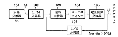
図9は、従来の画像形成装置におけるビデオクロック発生器の構成を説明するブロック図である。なお、ビデオクロック発生器はPLL(Phase Locked Loop)回路から構成される。
【0007】
図において、101は水晶発振器,102は1/M分周器,103は位相比較器,104はローパスフィルタ,105は電圧制御発振器(VCO),106は1/N分周器,14は出力信号であり、水晶発振器101から出力される。15はビデオクロックで、ビデオクロック発生器の出力であり、周波数が可変されたビデオクロックである。
【0008】
以下、ビデオクロック周波数の可変方法を説明する。水晶発振器101の出力信号14を1/M分周器102でM分周した信号と、ビデオクロック15を1/N分周器106でN分周した信号とを位相比較器103に入力し、位相比較器103の出力をローパスフィルタ104を通して電圧制御発振器105に入力する。
【0009】
例えば、水晶発振器101の出力信号14をM分周した信号の位相がビデオクロック15をN分周した信号の位相より進んでいた場合、電圧制御発振器105の入力電圧は上昇し、ビデオクロックの位相を進める。水晶発振器101の周波数をfin、ビデオクロック15の周波数をfoutとすると、
【0010】
【数2】
fout=fin×N/M ……(1)
となる。検出された主走査幅に応じてN/Mの値を調整することにより、ビデオクロック発生器から出力されるビデオクロック15の周波数は可変可能な構成となっている。
【0011】
例えば、上述の特公平6−57040号公報によれば、ビデオクロックを0.1%変化させたいときには分周器のカウンタは10ビット必要であると書かれている。また、ビデオクロックの可変最小周波数は、分周比で決定されるとも書かれている。すなわち、例えば、N/M=1000/1000→N/M=999/1000とすることで−0.1%の可変ステップを得るという方法である。
【0012】
この考え方に従えば、ビデオクロックを0.001%変化させたいときには、分周比を100000程度にしてやればよい。例えば、「基準色の主走査幅=300000μm(300mm)」,「調整色の主走査幅=300003μm」,「調整色のN/M=1」の場合、調整色のN/Mを「N/M=0.99999(−0.001%に相当)、例えば、N=99999,M=100000」とすれば良い。
【0013】
また、「基準色の主走査幅=300000μm(300mm)」,「調整色の主走査幅=299997μm」,「調整色のN/M=1」の場合には、調整色のN/MをN/M=1.00001(+0.001%に相当)、例えば、N=100001,M=100000とすればよい。
【0014】
【発明が解決しようとする課題】
ところが、Nが大きくなるにつれて、PLLのループの帰還量が小さくなる。上述した例のように、NがN≒100000で、foutがfout≒20MHzである場合には、位相比較器103への帰還はおおよそ5msecに一度しか行われない。
【0015】
このとき、VCO105自体のジッタが大きいと、帰還がかかったとき以外のジッタが悪化する。
【0016】
図10は、帰還量が小さい場合のビデオクロック15のジッタの悪化を説明する図である。
【0017】
図において、縦軸は、ビデオクロック15のジッタを示すものであり、横軸は、時間(msec)を示している。
【0018】
位相比較器103への帰還が5msecごとに行われるため、5msecごとにしかビデオクロック15のジッタが改善されない。ジッタが改善されていないときには、VCO105自体のジッタがでる。このように、PLL回路では、ジッタは基準クロックと同程度にまですることが可能であるが、上記のようにN≒100000にしたときには、帰還量が小さくなるためにジッタが基準クロックに比べて大きくなる。
【0019】
このように、上記従来の画像形成装置では、以下のような欠点があった。
【0020】
主走査倍率の補正精度を上げるために、主走査倍率可変ステップ量を小さくしようとすると、図9に示した分周器102,106のM,Nを大きな値にする必要がある。ところが、Nを大きな値にすると、PLLのループの帰還量が小さくなり、その結果、VCO105自体のジッタがビデオクロック15にジッタとして出てくるという問題点があった。さらに、ビデオクロック15のジッタは形成される画像に位置ずれや色ずれの形で表れてしまうという問題点があった。
【0021】
また、ビデオクロック15のジッタを小さくするには、PLL回路にジッタの小さなVCOを用いればよい。しかし、この場合には、コストが高くなるという問題点がある。
【0022】
本発明は、上記の問題点を解決するためになされたもので、本発明の目的は、ビデオクロックの周波数を所定の周波数可変ピッチ単位で可変させる場合に必要なピッチ数よりも小さい数を、前記第1分周手段および前記第2分周手段の分周比として設定することにより、ビデオクロックの周波数をより小さいピッチ単位で可変させた場合であっても、ビデオクロックのジッタを悪化させることなく高精度にビデオクロックを調整することができ、安価な構成で精度良く色ずれが補正された高品位な画像を得ることができる画像形成装置を提供することである。
【0023】
【課題を解決するための手段】
本発明に係る第1の発明は、複数の走査部を備える画像形成手段と、基準クロックを発生する1個以上の第1クロック発生手段と、前記基準クロックの周波数を前記各走査部毎に調整してビデオクロックを発生する複数の第2クロック発生手段とを有し、前記第2発生手段により発生した前記ビデオクロックに同期した画像信号に応じて前記各走査部が感光体を露光することにより画像形成する画像形成装置であって、前記各第2クロック発生手段は、前記基準クロックを分周する第1分周手段と、前記ビデオクロックを分周する第2分周手段と、前記第1分周手段で前記基準クロックを分周したクロックと前記第2分周手段で前記ビデオクロックを分周したクロックとの位相を比較し、該比較結果に応じた信号を出力する位相比較手段と、前記位相比較手段の出力の低周波成分を出力するフィルタ手段と、前記フィルタ手段からの電圧出力に応じた周波数のクロックを前記ビデオクロックとして出力する電圧制御発振手段と、前記各第2クロック発生手段の前記第1分周手段および前記第2分周手段の各分周比を変更して、前記ビデオクロックの周波数を可変する制御手段と、を有し、前記制御手段は、前記ビデオクロックの周波数を所定の周波数可変ピッチ単位のステップで可変させる場合に、前記周波数可変ピッチ単位で決定される最大ステップ数よりも小さい数を前記第1分周手段および前記第2分周手段の分周比として設定することを特徴とする。
【0024】
本発明に係る第2の発明は、前記制御手段は、前記ビデオクロックの周波数を前記所定の周波数可変ピッチ単位で増加させる場合、および前記ビデオクロックの周波数を前記所定の周波数可変ピッチ単位で減少させる場合に、前記分周比を前記第1分周手段および前記第2分周手段に設定することを特徴とする。
【0025】
本発明に係る第3の発明は、前記制御手段は、前記第1分周手段および前記第2分周手段に設定する分周比を所定の演算式に基づいて求めることを特徴とする。
【0026】
本発明に係る第4の発明は、前記制御手段は、前記第1分周手段および前記第2分周手段に設定する分周比を予め記憶されている前記第1分周手段と前記第2分周手段との分周比の組み合わせの中から選択することを特徴とする。
【0027】
本発明に係る第5の発明は、前記演算式とは、Mkを第1分周手段の分周比、Nkを第2分周手段の分周比、b,c,kを整数,No ,Mo を自然数とすると、
【数1】
Nk =No +kb
Mk =Mo +kc
で示されることを特徴とする。
【0035】
【発明の実施の形態】
以下、図面を参照して本発明の実施形態を詳細に説明する。
【0036】
〔第1実施形態〕
以下、図1を参照して、本発明の実施形態を示す画像形成装置の全体を説明する。
【0037】
図1は、本発明の第1実施形態を示す画像形成装置の概略構成を説明するブロック図である。本実施形態では、4色すなわちイエローY,マゼンタM,シアンC,ブラックKの画像形成部を備えたカラープリンタ等のカラー画像形成装置を一例に用いて説明する。
【0038】
図において、1a〜1dは感光ドラムであり、感光ドラム1aはブラックK,感光ドラム1bはシアンC,感光ドラム1cはマゼンタM,感光ドラム1dはイエローY用の静電潜像が形成される。2a〜2dは第1〜第4レーザスキャナで、画像信号に応じて露光を行い感光ドラム1a〜1d上に静電潜像を形成する。
【0039】
また、ブラック画像形成部は、感光ドラム1a,第1レーザスキャナ2a等から構成される。シアン画像形成部は、感光ドラム1b,第2レーザスキャナ2b等から構成される。マゼンタ画像形成部は、感光ドラム1c,第3レーザスキャナ2c等から構成される。イエロー画像形成部は、感光ドラム1d,第4レーザスキャナ2d等から構成される。
【0040】
3は無端状の搬送ベルトで、図示しない用紙を各色の画像形成部に順次搬送する転写ベルトを兼ねるものである。4は駆動ローラで、図示しないモータとギア等でなる駆動手段と接続され搬送ベルト3を駆動する。5は従動ローラで、搬送ベルト3の移動に従って回転し、かつ搬送ベルト3に一定の張力を付与する。6a,6bは1対の光センサで、搬送ベルト3の両サイドに設けられ、搬送ベルト3上に形成された位置ずれ検知用パターン(後述する図3に示す位置ずれ検出用パターン7a〜10a,7b〜10b等)を検出する。
【0041】
1000はコントローラで、CPU1001,RAM1002,ROM1003等から構成され、CPU1001はROM1003に格納される制御プログラムに基づいてカラープリンタを統括制御する。RAM1002はCPU1001のワークエリア等として使用される。
【0042】
以下、本実施形態の画像形成装置の動作について説明する。
【0043】
図示しないコンピュータ(PC)等からプリントすべきデータがカラープリンタに送られ、プリンタエンジンの方式に応じた画像処理が終了しプリンタ可能状態となると、図示しない用紙カセットから用紙が供給され搬送ベルト3に到達し、搬送ベルト3により用紙が各色の画像形成部に順次搬送される。
【0044】
搬送ベルト3による用紙搬送とタイミングを合せて、各色の画像信号が各レーザスキャナ2a〜2dに送られ、第1〜第4レーザスキャナ2a〜2dがレーザ光を照射して各感光ドラム1a〜1d上に静電潜像を形成し、図示しない現像器が各感光ドラム1a〜1d上に形成された静電潜像をトナーで現像し、図示しない転写部で感光ドラム1a〜1d上のトナー像を搬送ベルト3により搬送される用紙上に転写される。
【0045】
本実施形態で示すカラープリンタでは、Y,M,C,Kの順に順次画像形成される。その後、トナー像が転写された用紙は搬送ベルト3から分離され、図示しない定着器で熱によってトナー像が用紙上に定着され、外部へ排出される。
【0046】
以下、図2,図3を参照して、第1〜第4レーザスキャナ2a〜2dと感光ドラム1a〜1dとの距離が各画像形成部で異なる場合に発生する走査幅の誤差について説明する。
【0047】
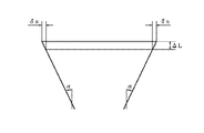
図2は、図1に示した第1〜第4スキャナユニット2a〜2dと感光ドラム1a〜1dとの距離が異なる場合の感光ドラム1a〜1d上での走査幅の誤差の一例を説明する図である。
【0048】
図において、αは入射角で、図1に示すスキャナユニット2(2a〜2d)から照射される走査レーザの感光ドラム1(1a〜1d)上への入射角である。ΔLはレーザスキャナ2と感光ドラム1間の距離誤差である。δsはαとΔLが原因で発生する走査幅の誤差であり、
【0049】
【数4】
δs=ΔL×tanα ……(1)
となる。例えば、ΔL=0.3mm、α=30度の場合、δs=173μmとなる。
【0050】
図3は、図1に示した搬送ベルト3により搬送される用紙に転写される画像で発生する走査幅の違いを説明する図である。
【0051】
図において、11は用紙で、図1に示した搬送ベルト3により搬送され、各画像形成部により各色のトナー画像が転写される。12は画像で、ある色、例えばブラック画像形成部で用紙11に転写された黒色の画像である。13は画像で、ある色とは別の色、例えばマゼンタ画像形成部で用紙11に転写されたマゼンタ色の画像である。
【0052】
例えば上述した条件と同様の場合、すなわちブラック画像形成部の感光ドラム1aとレーザスキャナ2aとの距離と、マゼンタ画像形成部の感光ドラム1cとレーザスキャナ2cとの距離との差がΔLである場合に、画像12と画像13の走査幅の誤差は、2×δs=346μmとなる。
【0053】
このように各画像形成部のレーザスキャナと感光ドラムとの距離が異なっている場合に、同一幅の画像を形成しようとしても用紙上には異なる幅の画像として形成されてしまう。
【0054】
この色ずれ(位置ずれ)を低減させる為、図1に示した搬送ベルト3上に後述する図4に示す様な位置ずれ検出用パターンを形成し、搬送ベルト3の両サイドに設けられた1対の光センサ6a,6bで読取り、各色の位置ずれ量を検出する。
【0055】
図4は、図1に示した搬送ベルト3等に転写される位置ずれ検出用パターンを説明する図である。
【0056】
図において、7a,7bは位置ずれ検出用パターンで、ブラック画像形成部により搬送ベルト3に転写されたレーザ走査方向と搬送方向に延びた直線パターンである。8a,8bは位置ずれ検出用パターンで、シアン画像形成部により搬送ベルト3に転写されたレーザ走査方向と搬送方向に延びた直線パターンである。
【0057】
9a,9bは位置ずれ検出用パターンで、マゼンタ画像形成部により搬送ベルト3に転写されたレーザ走査方向と搬送方向に延びた直線パターンである。10a,10bは位置ずれ検出用パターンで、イエロー画像形成部により搬送ベルト3に転写されたレーザ走査方向と搬送方向に延びた直線パターンである。
【0058】
なお、位置ずれ検出用パターン7a〜10aは、図1に示した搬送ベルト3の手前側のパターンであり、図1に示した光センサ6aで読み取られる。位置ずれ検出用パターン7b〜10bは、図1に示した搬送ベルト3の奥側のパターンであり、図1に示した光センサ6bで読み取られる。
【0059】
図1に示した光センサ6a,6bで読み取られた位置ずれ検出用パターンにより、図1に示したコントローラ1000がレーザ走査方向に延びた直線パターンから搬送方向の位置ずれ量を、搬送方向に延びた直線パターンからレーザ走査方向の位置ずれ量を検出する。なお、各色の走査幅は、搬送方向に延びた直線パターン7aと7b,8aと8b,9aと9b,10aと10b間の距離および光センサ6aと6bの間の距離から算出される。
【0060】
レーザ走査幅の補正は、後述する図5と図6に示す様に、各色毎に画像信号用のビデオクロック発生器を持ち、各色独立にビデオクロックの周波数を可変可能とし、周波数を調整することにより行う。
【0061】
図5は、図1に示した第1〜第4スキャナユニット2a〜2dに送出される画像信号の流れを説明する図である。
【0062】
図において、601は水晶発振器で、高精度な源クロック供給源であり、出力信号を第1〜第4ビデオクロック発生器602a〜602dに出力する。第1〜第4ビデオクロック発生器602a〜602dは後述する図6に示すような構成を有し、ビデオクロックを発生して第1〜第4画像データ制御部603a〜603dに出力する。
【0063】
第1〜第4画像データ制御部603a〜603dは第1〜第4ビデオクロック発生器602a〜602dからのビデオクロックの周波数に応じて画像信号を第1〜第4レーザスキャナ2a〜2dに出力する。第1〜第4レーザスキャナ2a〜2dは画像信号に応じてレーザを点灯制御する。
【0064】
このように、各色毎の第1〜第4ビデオクロック発生器602a〜602dから出力されるビデオクロックの周波数に応じて画像信号が第1〜第4レーザスキャナ2a〜2dに送られ、レーザが点灯制御される。
【0065】
図6は、図5に示した第1〜第4ビデオクロック発生器602a〜602dに備えられるPLL回路を説明するブロック図である。なお、図5と同一のものには同一の符号を付してある。
【0066】
図において、702は1/M分周器,703は位相比較器,704はローパスフィルタ,705は電圧制御発振器,706は1/N分周器であり、14は前記水晶発振器601からの出力信号、15は前記第1〜第4ビデオクロック発生器602a〜602dの出力で、可変されたビデオクロックである。
【0067】
700はビデオクロック周波数制御部であり、710はRAM,720はROMである。
【0068】
以下、第1〜第4ビデオクロック発生器602a〜602dにおけるビデオクロック周波数の可変方法を説明する。
【0069】
水晶発振器601の出力信号14を1/M分周器702でM分周した信号とビデオクロック15を1/N分周器706でN分周した信号とを位相比較器703に入力し、位相比較器703の出力をローパスフィルタ704を通して電圧制御発振器705に入力する。
【0070】
例えば、水晶発振器601の出力信号14をM分周した信号の位相がビデオクロック15をN分周した信号の位相より進んでいた場合、電圧制御発振器705の入力電圧は上昇し、ビデオクロック15の位相を進める。
【0071】
ここで、水晶発振器601からの出力信号14の周波数をfin、ビデオクロック15の周波数をfoutとすると、
【0072】
【数5】
fout=fin×N/M ……(2)
となる。
【0073】
検出された主走査幅に応じてN/Mの値を調整することにより、ビデオクロック周波数は可変可能な構成となっている。
【0074】
ここで、上述したように、Nの値を大きくするとジッタが大きくなるなどの不具合が生じる。そこで、本実施例では、次のようにすることで帰還量を増やし、ジッタを小さくする。
【0075】
例えば、「基準色の主走査幅=300000μm(300mm)」,「調整色の主走査幅=300003μm」,「調整色のN/M=952/949」の場合には、調整色のN/MをN/M=955/952とすればよい。
【0076】
また、「基準色の主走査幅=300000μm(300mm)」,「調整色の主走査幅=299997μm」,調整色のN/M=952/949の場合には、調整色のN/Mを、N/M=949/946とすればよい。このようにすることで、従来の技術の項に示したようにN≒100000にする場合に比べて、帰還量が100倍程度大きくなる。結果として、ジッタを小さくすることができる。
【0077】
上記のように2個の分周器702,706の分周比M,N両方を適切に変えることで、ジッタを大きくせずにビデオクロック周波数を微調することができる。
【0078】
以上の実施形態をもとにMとNの決定方法の一例について詳細に説明する。
【0079】
b,c,kを整数,No ,Mo を自然数とすると、1/M分周器702の分周比Kk 、1/N分周器706の分周比Nk は
【0080】
【数6】
Nk =No +kb
Kk =Mo +kc ……(3)
を演算することにより求められる。例えば、上記式(3)のb,c,Mo を「b=−3」,「c=−3」,「Mo =No +3」と定めると、
【0081】
【数7】
Nk =No −3k
Kk =No +3−3k
である。ここで、k=0とk=1のときを考えると、ビデオクロック周波数可変ピッチは、次式で表される。
【0082】
【数8】
{(N1 /M1 )−(No /Mo )}/(No /Mo ) ……(4)
ただし、M1 =No 、N1 =No −3である。
【0083】
上記実施形態では、所望のビデオクロック周波数可変ピッチは0.001%である。そこで、式(4)の絶対値が0.001%となるようNo,Mo計算すると、Noはおおよそ949となり、Moはおおよそ952となる。このとき、k=0からk=1になったとき、N1=946,M1=949となり、ビデオクロック周波数可変ピッチは、9.99ppmである。所望のビデオクロック周波数可変ピッチからのずれは0.01ppmである。所望のビデオクロック周波数可変ピッチが得られ、かつ、ビデオクロック周波数可変ピッチのずれが所望の範囲になるように、上記式(3)の各変数の値を決めていく。
【0084】
〔第2実施形態〕
上記第1実施形態では、数列を演算することにより各分周器の分周比M,Nを求める場合を説明したが、各分周器の分周比M,Nの組み合わせを予め計算してメモリに記憶させ、該記憶される分周比の組み合わせを必要に応じて読み取り、ビデオクロック周波数を変更するように構成してもよい。以下、その実施形態について説明する。
【0085】
なお、本実施形態の画像形成装置においても、上記第1実施形態同様の構成を有している。
【0086】
以下、図7を参照して、ビデオクロック周波数可変ステップ(ピッチ)を35ppmとしたときのMとNの組合わせの一例を説明する。
【0087】
図7は、図6に示したROM720等に格納される分周比の組み合わせテーブルの一例を説明する図である。
【0088】
左側の欄に分周比M,Nの組み合わせ、右側の欄には分周比を変更したときのビデオクロック周波数可変ステップを示している。
【0089】
予め、このような分周比M,Nの組み合わせを計算しておき、図5に示したRAM710,ROM720,図示しないハードディスク等のメモリに記録しておく。このメモリから必要に応じてMとNの値を読み取り、ビデオクロック周波数を変える。
【0090】
例えば、M=1134、N=1168であった場合を考える。ここで主走査幅を35ppm小さくする必要があれば、図6に示したビデオクロック周波数制御手段700は、ROM720からM=1066,N=1098を読み取り、その値を1/M分周器702,1/N分周器706に設定すればよい。逆に主走査幅を35ppm大きくする必要があれば、ビデオクロック周波数制御手段700はROM720からM=935,N=963を読み取り、その値を1/M分周器702,1/N分周器706に設定すればよい。
【0091】
メモリに記録する分周比MとNとの組み合わせを多くすれば、ビデオクロック周波数の可変範囲を広く取ることができる。
【0092】
以下、図8のフローチャートを参照して、画像形成装置のレーザ走査幅の調整処理手順について説明する。
【0093】
図8は、本発明に係る画像形成装置における第1のデータ処理手順の一例を説明するフローチャートである。なお、(1)〜(2)は各ステップを示す。
【0094】
まず、図6に示したビデオクロック周波数制御手段700は、所望のビデオクロック周波数可変ピッチに適した1/M分周器702,1/N分周器706の分周比M,Nの組み合わせを求める(1)。なお、ステップ(1)では、上述したように数列を演算することにより分周比M,Nの組み合わせを求めても良いし、予め記憶される分周比の組み合わせの中から適切な分周比M,Nの組み合わせを選択しても良い。
【0095】
次に、1/M分周器702,1/N分周器706の分周比をステップ(1)で選択した分周比に変更し(2)、処理を終了する。
【0096】
このように処理を行うことにより、ジッタを悪化させることなく、ビデオクロックの周波数を微調することができ、各画像形成部で形成される画像の位置ずれを軽減して、高品質な画像を得ることができる。
【0097】
〔その他の実施形態〕
上記各実施形態において、主走査幅の補正は適切なときに行う。例えば、紙間、温湿度などの環境が変わったとき、一定時間経過したとき、画像形成装置の立ち上げ時、工場での出荷前調整のときなどに行うことで効果を得ることができる。工場での出荷前調整では、光学部品やスキャナなどの機械的な調整よりも低いコストでの調整が期待できる。
【0098】
上記各実施形態では、4色の画像形成部からなる構成について説明した。しかし、2色や3色の画像形成部からなる構成でも本発明は有効である。また、5色以上の画像形成部からなる構成においても本発明は有効である。
【0099】
また、上記各実施形態では、N/Mが1に近い場合について説明した。しかし、N/M≒1ではない場合にも本構成は有効である。例えば、N/M≒4とすることで、ビデオクロックのおおよそ1/4の周波数の基準クロックで、所望のビデオクロックを得ることができる。
【0100】
上記各実施形態では、分周器が2個からなる構成について説明した。ただし、分周器は2個である必要はなく、機能として、基準クロック分周手段と、電圧制御発振器クロック分周手段の2個あればよい。例えば、電圧制御発振器クロック分周手段としてプリスケーラを用いた場合には、電圧制御発振器クロック分周手段は2個以上の分周器から構成されることになる。さらに、パルス・スワロウ・カウンタのように、2個以上の分周器で1個の分周器の働きをする装置などを使った場合などでも、本構成の有効性は変わらない。
【0101】
さらに、上記各実施形態では、図4に示したような主走査と副走査方向の直線からなる位置ずれ検出パターンにより各画像形成部により形成される画像の位置ずれを検出する場合について説明した。ただし、これ以外のパターンであっても、主走査方向および副走査方向の位置ずれを検出できるパターンであれば他のパターンを用いても本発明は有効である。
【0102】
また、上記各実施形態では、搬送ベルト上にレジ検知パターンを形成する例をあげた。しかし、この例に限らず、例えばベルト上に画像を形成し、しかる後に紙などの画像記録媒体に画像を転写する装置のベルトやドラム、すなわち中間転写ベルトや中間転写ドラムにレジ検知パターンを形成した場合にも、本発明は、有効である。
【0103】
上記各実施形態では、主走査倍率が変化する原因としてスキャナと感光体との距離がずれることを挙げた。しかし、この原因に限らず、例えば光学部品の位置ずれやレンズ等の屈折率の変化や変形などの理由により、主走査倍率が変化した場合の補正にも、本発明は有効である。
【0104】
さらに、上記各実施形態では、主走査倍率の補正のために本構成を用いた。しかし、画像倍率を調整したい場合など、積極的に主走査倍率を調整するように構成しても有効である。この場合は、記録媒体の搬送速度を調整して副走査方向の倍率も変えることで、主走査方向、副走査方向共に画像倍率を調整することもできる。
【0105】
また上記各実施形態では、レーザスキャナ光学系と感光体とが一対一で対応している構成を示した。しかし、レーザスキャナ光学系と感光体とは一対一で対応していない場合にも本発明は適用できる。例えば、無端状の感光体やドラム状の感光体を使うことにより、複数のレーザスキャナ光学系と1個の感光体により画像形成部を構成することができる。この場合でも本発明は有効である。
【0106】
このように、上記各実施形態で示した画像形成装置は、各レーザスキャナ光学系(第1〜第4レーザスキャナ2a〜2d)に個別に設けられた第1〜第4ビデオクロック発生器602a〜602dに含まれる分周器702,706の分周比をビデオクロック周波数制御手段700によって可変することにより、ビデオクロック周波数を変えることができる。
【0107】
このようにして、周波数を変えたビデオクロックに同期した画像信号で変調されたビームにより感光ドラム1a〜1dを露光することで、感光体上における走査幅を変えることができ、各レーザスキャナ光学系のばらつきによる走査幅の誤差を補正できる。さらに走査幅の補正をすることで、各画像形成部で形成される画像の色ずれや位置ずれの補正をすることができる。
【0108】
この際に、上述したように電圧制御発振器705の出力を分周する1/N分周器706と1/M分周器702の各分周比M,Nの両方を変えることで、第1〜第4ビデオクロック発生器602a〜602dに含まれる帰還回路の帰還量を大きくしたまま、ビデオクロック周波数の微調が可能となるため、安価に高精度に色ずれや位置ずれを補正することができ、高画質化を図れる。
【0109】
また、上記各実施形態を組合せて実施するように構成してもよい。
【0110】
さらに、上記各実施形態では、画像形成装置を一例に挙げて説明しているが、種々の画像形成装置、例えば電子写真装置,デジタル複写機,モノクロ複写機,カラーレーザ複写機,レーザビームプリンタ,カラーレーザプリンタ,ファクシミリ装置,コピー機能および/またはプリント機能および/またはファクシミリ機能等を備える複合複写機等、および種々の画像形成装置を制御する制御装置,情報処理装置,データ処理装置等に対し本実施形態で示した技術を適用するように構成してもよい。
【0111】
以上のように、前述した実施形態の機能を実現するソフトウエアのプログラムコードを記録した記憶媒体を、システムあるいは装置に供給し、そのシステムあるいは装置のコンピュータ(またはCPUやMPU)が記憶媒体に格納されたプログラムコードを読出して実行することによっても、本発明の目的が達成されることは言うまでもない。
【0112】
この場合、記憶媒体から読み出されたプログラムコード自体が本発明の新規な機能を実現することになり、そのプログラムコードを記憶した記憶媒体は本発明を構成することになる。
【0113】
プログラムコードを供給するための記憶媒体としては、例えば、フロッピーディスク,ハードディスク,光ディスク,光磁気ディスク,CD−ROM,CD−R,磁気テープ,不揮発性のメモリカード,ROM,EEPROM等を用いることができる。
【0114】
また、コンピュータが読み出したプログラムコードを実行することにより、前述した実施形態の機能が実現されるだけでなく、そのプログラムコードの指示に基づき、コンピュータ上で稼働しているOS(オペレーティングシステム)等が実際の処理の一部または全部を行い、その処理によって前述した実施形態の機能が実現される場合も含まれることは言うまでもない。
【0115】
さらに、記憶媒体から読み出されたプログラムコードが、コンピュータに挿入された機能拡張ボードやコンピュータに接続された機能拡張ユニットに備わるメモリに書き込まれた後、そのプログラムコードの指示に基づき、その機能拡張ボードや機能拡張ユニットに備わるCPU等が実際の処理の一部または全部を行い、その処理によって前述した実施形態の機能が実現される場合も含まれることは言うまでもない。
【0116】
また、本発明は、複数の機器から構成されるシステム、例えば,印刷システム,画像処理システム,画像形成システム,制御システム,印刷制御システム,画像処理制御システム,画像形成制御システム等に適用しても、1つの機器からなる装置,例えば,印刷装置,画像処理装置,画像形成装置,制御装置,印刷制御装置,画像処理制御装置,画像形成制御装置等に適用してもよい。また、本発明は、システムあるいは装置にプログラムを供給することによって達成される場合にも適応できることは言うまでもない。この場合、本発明を達成するためのソフトウエアによって表されるプログラムを格納した記憶媒体を該システムあるいは装置に読み出すことによって、そのシステムあるいは装置が、本発明の効果を享受することが可能となる。
【0117】
さらに、本発明を達成するためのソフトウエアによって表されるプログラムをネットワーク上のデータベースから通信プログラムによりダウンロードして読み出すことによって、そのシステムあるいは装置が、本発明の効果を享受することが可能となる。
【0118】
【発明の効果】
以上説明したように、本発明によれば、ビデオクロックの周波数を所定の周波数可変ピッチ単位で可変させる場合に必要なピッチ数よりも小さい数を、前記第1分周手段および前記第2分周手段の分周比として設定することにより、ビデオクロックの周波数をより小さいピッチ単位で可変させた場合であっても、ビデオクロックのジッタを悪化させることなく高精度にビデオクロックを調整することができ、安価な構成で精度良く色ずれが補正された高品位な画像を得ることができるという効果を奏する。
【図面の簡単な説明】
【図1】本発明の第1実施形態を示す画像形成装置の概略構成を説明するブロック図である。
【図2】図1に示した第1〜第4スキャナユニットと感光ドラムとの距離が異なる場合の感光ドラム上での走査幅の誤差の一例を説明する図である。
【図3】図1に示した搬送ベルトにより搬送される用紙に転写される画像で発生する走査幅の違いを説明する図である。
【図4】図1に示した搬送ベルト等に転写される位置ずれ検出用パターンを説明する図である。
【図5】図1に示した第1〜第4スキャナユニットに送出される画像信号の流れを説明する図である。
【図6】図5に示した第1〜第4ビデオクロック発生器に備えられるPLL回路を説明するブロック図である。
【図7】図6に示したROM等に格納される分周比の組み合わせテーブルの一例を説明する図である。
【図8】本発明に係る画像形成装置における第1のデータ処理手順の一例を説明するフローチャートである。
【図9】従来の画像形成装置におけるビデオクロック発生器の構成を説明するブロック図である。
【図10】帰還量が小さい場合のビデオクロックのジッタの悪化を説明する図である。
【符号の説明】
1a〜1d 感光ドラム
2a〜2d 第1〜第4レーザスキャナ
3 搬送ベルト
6a,6b 光センサ
7a、7b〜10a,10b 位置ずれ検出用パターン
601 水晶発振器
700 ビデオクロック周波数制御手段
702 1/M分周器
703 位相比較器
704 ローパスフィルタ
705 電圧制御発振器
706 1/N分周器
1000 コントローラ[0001]
BACKGROUND OF THE INVENTION
The present invention relates to an image forming apparatus that forms an image by exposing a photosensitive member to a photoconductor in accordance with an image signal synchronized with a video clock adjusted for each of a plurality of scanning units.
[0002]
[Prior art]
Conventional image forming apparatuses such as electrophotographic color printers and color copiers have a plurality of image forming units for outputting color images at high speed, and are formed on the photosensitive drums of the image forming units. Various methods for sequentially transferring toner images of different colors onto a recording material held on a conveying belt have been proposed.
[0003]
In such a conventional image forming apparatus having a plurality of image forming units, due to machine accuracy or the like, the photosensitive drums or the conveyance belts of the plurality of image forming units have uneven rotation or movement, and the transfer positions of the image forming units. The amount of movement between the outer peripheral surface of the photosensitive drum and the transport belt in the image forming apparatus is different for each image forming unit, and the toner images of each color formed on the photosensitive drum of each image forming unit are transferred to a recording material. Sometimes, the toner images of the respective colors do not match and color misregistration (positional misregistration) occurs.
[0004]
In particular, in an image forming apparatus having a plurality of image forming units having a laser scanner and a photosensitive drum, there is an error in the distance between the laser scanner and the photosensitive drum in the image forming unit, and if this error differs between the image forming units, A difference occurs in the scanning width of the laser on the photosensitive drum of each image forming unit, and a color shift (position shift) occurs.
[0005]
In order to reduce this color misregistration (positional misregistration), as shown in FIG. 9 to be described later, a video clock generator for image signals is provided for each color, and the frequency of the video clock can be varied independently for each color. An image forming apparatus that corrects the laser scanning width by adjusting the frequency has been proposed (for example, disclosed in Japanese Patent Publication No. 6-57040).
[0006]
FIG. 9 is a block diagram illustrating a configuration of a video clock generator in a conventional image forming apparatus. The video clock generator is composed of a PLL (Phase Locked Loop) circuit.
[0007]
In the figure, 101 is a crystal oscillator, 102 is a 1 / M frequency divider, 103 is a phase comparator, 104 is a low pass filter, 105 is a voltage controlled oscillator (VCO), 106 is a 1 / N frequency divider, and 14 is an output signal. And output from the
[0008]
Hereinafter, a method for changing the video clock frequency will be described. A signal obtained by dividing the
[0009]
For example, when the phase of the signal obtained by dividing the
[0010]
[Expression 2]
fout = fin × N / M (1)
It becomes. By adjusting the value of N / M according to the detected main scanning width, the frequency of the
[0011]
For example, according to the above Japanese Patent Publication No. 6-57040, it is written that the counter of the frequency divider needs 10 bits when it is desired to change the video clock by 0.1%. It is also written that the variable minimum frequency of the video clock is determined by the division ratio. That is, for example, by setting N / M = 1000/1000 → N / M = 999/1000, a variable step of −0.1% is obtained.
[0012]
According to this idea, when the video clock is to be changed by 0.001%, the frequency division ratio may be set to about 100,000. For example, when “main scanning width of reference color = 300,000 μm (300 mm)”, “main scanning width of adjustment color = 30,0003 μm”, and “N / M of adjustment color = 1”, N / M of the adjustment color is set to “N / M M = 0.99999 (corresponding to −0.001%), for example, N = 99999, M = 100000 ”.
[0013]
Further, when “main scanning width of reference color = 300000 μm (300 mm)”, “main scanning width of adjustment color = 299997 μm”, and “N / M of adjustment color = 1”, N / M of the adjustment color is set to N /M=1.0001 (corresponding to + 0.001%), for example, N = 100001 and M = 100000.
[0014]
[Problems to be solved by the invention]
However, as N increases, the feedback amount of the PLL loop decreases. As in the above-described example, when N is N≈100,000 and fout is fout≈20 MHz, feedback to the
[0015]
At this time, if the jitter of the VCO 105 itself is large, jitter other than when feedback is applied deteriorates.
[0016]
FIG. 10 is a diagram for explaining the deterioration of the jitter of the
[0017]
In the figure, the vertical axis represents the jitter of the
[0018]
Since feedback to the
[0019]
As described above, the conventional image forming apparatus has the following drawbacks.
[0020]
To reduce the main scanning magnification variable step amount in order to increase the correction accuracy of the main scanning magnification, it is necessary to increase M and N of the
[0021]
In order to reduce the jitter of the
[0022]
The present invention has been made to solve the above problems, and the object of the present invention is to reduce the number of pitches smaller than the number of pitches required when the frequency of the video clock is varied in units of a predetermined frequency variable pitch. By setting the frequency dividing ratio of the first frequency dividing means and the second frequency dividing means, the video clock jitter is deteriorated even when the frequency of the video clock is varied in smaller pitch units. The present invention provides an image forming apparatus capable of adjusting a video clock with high accuracy and obtaining a high-quality image with accurate color correction with an inexpensive configuration.
[0023]
[Means for Solving the Problems]
According to a first aspect of the present invention, an image forming unit including a plurality of scanning units, one or more first clock generating units that generate a reference clock, and a frequency of the reference clock are adjusted for each of the scanning units. A plurality of second clock generating means for generating a video clock, and each scanning section exposes the photosensitive member in accordance with an image signal synchronized with the video clock generated by the second generating means. An image forming apparatus for forming an image, wherein each of the second clock generators includes a first divider for dividing the reference clock, a second divider for dividing the video clock, and the first Phase comparison means for comparing the phases of the clock obtained by dividing the reference clock by the frequency dividing means and the clock obtained by dividing the video clock by the second frequency dividing means, and outputting a signal corresponding to the comparison result; Filter means for outputting a low frequency component of the output of the phase comparison means, voltage controlled oscillation means for outputting a clock having a frequency corresponding to the voltage output from the filter means as the video clock, and each second clock generating means Control means for changing the frequency ratio of the video clock by changing the frequency dividing ratios of the first frequency dividing means and the second frequency dividing means, and the control means has a frequency of the video clock. Is made variable in steps of a predetermined frequency variable pitch unit, a number smaller than the maximum step number determined in the frequency variable pitch unit is used as the frequency dividing ratio of the first frequency dividing unit and the second frequency dividing unit. It is characterized by setting.
[0024]
According to a second aspect of the present invention, the control means increases the frequency of the video clock in the predetermined frequency variable pitch unit, and decreases the video clock frequency in the predetermined frequency variable pitch unit. In this case, the frequency dividing ratio is set in the first frequency dividing means and the second frequency dividing means.
[0025]
A third invention according to the present invention is characterized in that the control means obtains a frequency division ratio set in the first frequency dividing means and the second frequency dividing means based on a predetermined arithmetic expression.
[0026]
According to a fourth aspect of the present invention, the control means stores the first frequency division means and the second frequency division ratio that are preliminarily stored in the frequency division ratios set in the first frequency division means and the second frequency division means. It is characterized by selecting from combinations of frequency division ratios with frequency dividing means.
[0027]
According to a fifth aspect of the present invention, the arithmetic expression is MkIs the frequency dividing ratio of the first frequency dividing means, NkIs the frequency dividing ratio of the second frequency dividing means, b, c, k are integers, No , Mo Is a natural number
[Expression 1]
Nk = No + Kb
Mk = Mo + Kc
It is characterized by being shown by.
[0035]
DETAILED DESCRIPTION OF THE INVENTION
Hereinafter, embodiments of the present invention will be described in detail with reference to the drawings.
[0036]
[First Embodiment]
Hereinafter, with reference to FIG. 1, the entire image forming apparatus showing an embodiment of the present invention will be described.
[0037]
FIG. 1 is a block diagram illustrating a schematic configuration of an image forming apparatus according to a first embodiment of the present invention. In the present embodiment, a color image forming apparatus such as a color printer having an image forming unit of four colors, that is, yellow Y, magenta M, cyan C, and black K will be described as an example.
[0038]
In the figure, reference numerals 1a to 1d denote photosensitive drums, in which electrostatic latent images for black K are formed for the photosensitive drum 1a, cyan C for the photosensitive drum 1b, magenta M for the photosensitive drum 1c, and yellow Y for the
[0039]
The black image forming unit includes a photosensitive drum 1a, a
[0040]
[0041]
A
[0042]
Hereinafter, the operation of the image forming apparatus of this embodiment will be described.
[0043]
When data to be printed is sent from a computer (PC) or the like (not shown) to the color printer and image processing according to the system of the printer engine is completed and the printer is ready, paper is supplied from a paper cassette (not shown) to the
[0044]
The image signals of the respective colors are sent to the
[0045]
In the color printer shown in this embodiment, images are sequentially formed in the order of Y, M, C, and K. Thereafter, the sheet on which the toner image has been transferred is separated from the
[0046]
Hereinafter, with reference to FIG. 2 and FIG. 3, a description will be given of an error in scanning width that occurs when the distance between the first to
[0047]
FIG. 2 is a diagram for explaining an example of an error in scanning width on the photosensitive drums 1a to 1d when the distances between the first to
[0048]
In the figure, α is an incident angle, which is an incident angle of the scanning laser irradiated from the scanner unit 2 (2a to 2d) shown in FIG. 1 onto the photosensitive drum 1 (1a to 1d). ΔL is a distance error between the laser scanner 2 and the
[0049]
[Expression 4]
δs = ΔL × tan α (1)
It becomes. For example, when ΔL = 0.3 mm and α = 30 degrees, δs = 173 μm.
[0050]
FIG. 3 is a diagram for explaining a difference in scanning width occurring in an image transferred to a sheet conveyed by the conveying
[0051]
In the figure, reference numeral 11 denotes paper, which is transported by the
[0052]
For example, in the same condition as described above, that is, when the difference between the distance between the photosensitive drum 1a of the black image forming unit and the
[0053]
As described above, when the distance between the laser scanner of each image forming unit and the photosensitive drum is different, even if an image having the same width is formed, an image having a different width is formed on the sheet.
[0054]
In order to reduce the color misregistration (positional misalignment), a misregistration detection pattern as shown in FIG. 4 to be described later is formed on the conveying
[0055]
FIG. 4 is a diagram for explaining a misregistration detection pattern transferred to the
[0056]
In the figure,
[0057]
[0058]
The
[0059]
By the misalignment detection patterns read by the
[0060]
As shown in FIGS. 5 and 6, which will be described later, the laser scanning width is corrected by having a video clock generator for an image signal for each color, making the frequency of the video clock variable for each color, and adjusting the frequency. To do.
[0061]
FIG. 5 is a diagram for explaining the flow of image signals sent to the first to
[0062]
In the figure,
[0063]
The first to fourth image
[0064]
As described above, the image signal is sent to the first to
[0065]
FIG. 6 is a block diagram illustrating a PLL circuit provided in the first to fourth
[0066]
In the figure, 702 is a 1 / M frequency divider, 703 is a phase comparator, 704 is a low pass filter, 705 is a voltage controlled oscillator, 706 is a 1 / N frequency divider, and 14 is an output signal from the
[0067]
[0068]
Hereinafter, a method of changing the video clock frequency in the first to fourth
[0069]
A signal obtained by dividing the
[0070]
For example, when the phase of the signal obtained by dividing the
[0071]
Here, if the frequency of the
[0072]
[Equation 5]
fout = fin × N / M (2)
It becomes.
[0073]
The video clock frequency can be varied by adjusting the value of N / M in accordance with the detected main scanning width.
[0074]
Here, as described above, increasing the value of N causes problems such as an increase in jitter. Therefore, in this embodiment, the feedback amount is increased and the jitter is reduced by the following.
[0075]
For example, when “main scanning width of reference color = 300,000 μm (300 mm)”, “main scanning width of adjustment color = 30,0003 μm”, “N / M of adjustment color = 952/949”, N / M of adjustment color N / M = 955/952.
[0076]
In the case of “main scanning width of reference color = 300,000 μm (300 mm)”, “main scanning width of adjustment color = 299997 μm”, and N / M of adjustment color = 952/949, N / M of adjustment color is N / M = 949/946 may be set. By doing so, the feedback amount becomes about 100 times larger than the case where N≈100,000 as shown in the prior art section. As a result, jitter can be reduced.
[0077]
As described above, by appropriately changing both the frequency division ratios M and N of the two
[0078]
An example of a method for determining M and N will be described in detail based on the above embodiment.
[0079]
b, c, k are integers, No , Mo Is a natural number, the frequency division ratio K of the 1 /
[0080]
[Formula 6]
Nk = No + Kb
Kk = Mo + Kc (3)
Is obtained by calculating. For example, b, c, M in the above formula (3)o "B = -3", "c = -3", "Mo = No +3 ”
[0081]
[Expression 7]
Nk = No -3k
Kk = No + 3-3k
It is. Here, considering the case of k = 0 and k = 1, the video clock frequency variable pitch is expressed by the following equation.
[0082]
[Equation 8]
{(N1 / M1 )-(No / Mo )} / (No / Mo ) (4)
However, M1 = No , N1 = No -3.
[0083]
In the above embodiment, the desired video clock frequency variable pitch is 0.001%. Therefore, when No and Mo are calculated so that the absolute value of Equation (4) is 0.001%, No is approximately 949 and Mo is approximately 952. At this time, when k = 0 to k = 1, N1 = 946 and M1 = 949, and the video clock frequency variable pitch is 9.99 ppm. Deviation from the desired video clock frequency variable pitch is 0.01 ppm. The value of each variable of the above equation (3) is determined so that a desired video clock frequency variable pitch can be obtained and the deviation of the video clock frequency variable pitch falls within a desired range.
[0084]
[Second Embodiment]
In the first embodiment, the case has been described in which the frequency division ratios M and N of the frequency dividers are obtained by calculating several sequences, but the combination of the frequency division ratios M and N of the frequency dividers is calculated in advance. It may be configured to store in a memory, read the combination of the division ratios stored as necessary, and change the video clock frequency. The embodiment will be described below.
[0085]
Note that the image forming apparatus of the present embodiment also has a configuration similar to that of the first embodiment.
[0086]
Hereinafter, an example of a combination of M and N when the video clock frequency variable step (pitch) is set to 35 ppm will be described with reference to FIG.
[0087]
FIG. 7 is a diagram for explaining an example of a combination table of frequency division ratios stored in the
[0088]
The left column shows the combination of the division ratios M and N, and the right column shows the video clock frequency variable step when the division ratio is changed.
[0089]
Such a combination of the frequency division ratios M and N is calculated in advance and recorded in a memory such as the
[0090]
For example, consider the case where M = 1134 and N = 1168. Here, if it is necessary to reduce the main scanning width by 35 ppm, the video clock frequency control means 700 shown in FIG. 6 reads M = 1066, N = 1098 from the
[0091]
If the combination of the frequency division ratios M and N recorded in the memory is increased, the variable range of the video clock frequency can be widened.
[0092]
Hereinafter, the procedure for adjusting the laser scanning width of the image forming apparatus will be described with reference to the flowchart of FIG.
[0093]
FIG. 8 is a flowchart for explaining an example of the first data processing procedure in the image forming apparatus according to the present invention. In addition, (1)-(2) shows each step.
[0094]
First, the video clock frequency control means 700 shown in FIG. 6 uses a combination of the frequency division ratios M and N of the 1 /
[0095]
Next, the frequency division ratio of the 1 /
[0096]
By performing the processing in this manner, the frequency of the video clock can be finely adjusted without deteriorating the jitter, the positional deviation of the image formed in each image forming unit is reduced, and a high quality image is obtained. be able to.
[0097]
[Other Embodiments]
In each of the above embodiments, the main scanning width is corrected when appropriate. For example, the effect can be obtained when the environment such as the interval between papers, temperature and humidity changes, when a certain period of time has passed, when starting up the image forming apparatus, or when making adjustments before shipment at the factory. In factory pre-shipment adjustment, adjustment at a lower cost than mechanical adjustment of optical components and scanners can be expected.
[0098]
In each of the above-described embodiments, the configuration including the four-color image forming units has been described. However, the present invention is effective even in a configuration including two-color or three-color image forming units. The present invention is also effective in a configuration including image forming units of five or more colors.
[0099]
In each of the above embodiments, the case where N / M is close to 1 has been described. However, this configuration is effective even when N / M≈1 is not satisfied. For example, by setting N / M≈4, a desired video clock can be obtained with a reference clock having a frequency that is approximately ¼ of the video clock.
[0100]
In each of the above embodiments, the configuration including two frequency dividers has been described. However, the number of frequency dividers does not have to be two, and only two functions of a reference clock frequency dividing unit and a voltage controlled oscillator clock frequency dividing unit may be used as functions. For example, when a prescaler is used as the voltage controlled oscillator clock dividing means, the voltage controlled oscillator clock dividing means is composed of two or more frequency dividers. Furthermore, the effectiveness of this configuration does not change even when a device such as a pulse swallow counter that functions as one frequency divider with two or more frequency dividers is used.
[0101]
Further, in each of the above-described embodiments, the case has been described in which the positional deviation of the image formed by each image forming unit is detected by the positional deviation detection pattern including the straight lines in the main scanning and sub-scanning directions as shown in FIG. However, the present invention is effective even if other patterns are used as long as they are patterns that can detect positional deviation in the main scanning direction and the sub-scanning direction.
[0102]
In each of the above embodiments, an example in which the registration detection pattern is formed on the conveyance belt has been described. However, the present invention is not limited to this example. For example, a registration detection pattern is formed on a belt or drum of an apparatus that forms an image on a belt and then transfers the image onto an image recording medium such as paper, that is, an intermediate transfer belt or an intermediate transfer drum. Even in this case, the present invention is effective.
[0103]
In each of the above embodiments, the cause of the change in the main scanning magnification is that the distance between the scanner and the photosensitive member is shifted. However, the present invention is not limited to this cause, and the present invention is also effective for correction when the main scanning magnification changes due to, for example, a positional shift of an optical component or a change or deformation of a refractive index of a lens or the like.
[0104]
Furthermore, in each of the above embodiments, this configuration is used for correcting the main scanning magnification. However, it is effective to adjust the main scanning magnification positively when it is desired to adjust the image magnification. In this case, the image magnification can be adjusted in both the main scanning direction and the sub-scanning direction by adjusting the conveyance speed of the recording medium and changing the magnification in the sub-scanning direction.
[0105]
In each of the above-described embodiments, the configuration in which the laser scanner optical system and the photoconductor are in one-to-one correspondence is shown. However, the present invention can also be applied when the laser scanner optical system and the photosensitive member do not correspond one-to-one. For example, by using an endless photoreceptor or a drum-shaped photoreceptor, an image forming unit can be configured by a plurality of laser scanner optical systems and one photoreceptor. Even in this case, the present invention is effective.
[0106]
As described above, the image forming apparatus described in each of the above embodiments includes the first to fourth
[0107]
In this way, by exposing the photosensitive drums 1a to 1d with the beam modulated with the image signal synchronized with the video clock whose frequency is changed, the scanning width on the photosensitive member can be changed, and each laser scanner optical system It is possible to correct an error in the scanning width due to variations in the number. Further, by correcting the scanning width, it is possible to correct the color shift and the position shift of the image formed by each image forming unit.
[0108]
At this time, as described above, the first and second frequency division ratios M and N of the 1 /
[0109]
Moreover, you may comprise so that it may implement combining said each embodiment.
[0110]
Further, in each of the above embodiments, the image forming apparatus is described as an example, but various image forming apparatuses such as an electrophotographic apparatus, a digital copying machine, a monochrome copying machine, a color laser copying machine, a laser beam printer, This book is for color laser printers, facsimile machines, composite copiers with copy and / or print functions and / or facsimile functions, etc., and control devices, information processing devices, data processing devices, etc. for controlling various image forming devices. You may comprise so that the technique shown by embodiment may be applied.
[0111]
As described above, a storage medium storing software program codes for realizing the functions of the above-described embodiments is supplied to the system or apparatus, and the computer (or CPU or MPU) of the system or apparatus stores the storage medium in the storage medium. It goes without saying that the object of the present invention can also be achieved by reading and executing the program code.
[0112]
In this case, the program code itself read from the storage medium realizes the novel function of the present invention, and the storage medium storing the program code constitutes the present invention.
[0113]
As a storage medium for supplying the program code, for example, a floppy disk, a hard disk, an optical disk, a magneto-optical disk, a CD-ROM, a CD-R, a magnetic tape, a nonvolatile memory card, a ROM, an EEPROM, or the like is used. it can.
[0114]
Further, by executing the program code read by the computer, not only the functions of the above-described embodiments are realized, but also an OS (operating system) or the like running on the computer based on the instruction of the program code. It goes without saying that a case where the function of the above-described embodiment is realized by performing part or all of the actual processing and the processing is included.
[0115]
Further, after the program code read from the storage medium is written to a memory provided in a function expansion board inserted into the computer or a function expansion unit connected to the computer, the function expansion is performed based on the instruction of the program code. It goes without saying that the case where the CPU or the like provided in the board or the function expansion unit performs part or all of the actual processing and the functions of the above-described embodiments are realized by the processing.
[0116]
The present invention may also be applied to a system composed of a plurality of devices, such as a printing system, an image processing system, an image forming system, a control system, a printing control system, an image processing control system, and an image forming control system. You may apply to the apparatus which consists of one apparatus, for example, a printing apparatus, an image processing apparatus, an image forming apparatus, a control apparatus, a printing control apparatus, an image processing control apparatus, an image formation control apparatus etc. Needless to say, the present invention can be applied to a case where the present invention is achieved by supplying a program to a system or apparatus. In this case, by reading the storage medium storing the program represented by the software for achieving the present invention into the system or apparatus, the system or apparatus can enjoy the effects of the present invention. .
[0117]
Furthermore, by downloading and reading a program represented by software for achieving the present invention from a database on a network by a communication program, the system or apparatus can enjoy the effects of the present invention. .
[0118]
【The invention's effect】
As described above, according to the present invention, a number smaller than the number of pitches required for changing the frequency of the video clock in a predetermined frequency variable pitch unit is set to the first frequency dividing means and the second frequency divided. By setting the frequency division ratio, the video clock can be adjusted with high accuracy without deteriorating the jitter of the video clock, even when the video clock frequency is varied in smaller pitch units. Thus, it is possible to obtain a high-quality image in which color misregistration is accurately corrected with an inexpensive configuration.
[Brief description of the drawings]
FIG. 1 is a block diagram illustrating a schematic configuration of an image forming apparatus according to a first embodiment of the present invention.
2 is a diagram illustrating an example of an error in scanning width on a photosensitive drum when the distance between the first to fourth scanner units shown in FIG. 1 and the photosensitive drum is different. FIG.
FIG. 3 is a diagram illustrating a difference in scanning width that occurs in an image transferred to a sheet conveyed by the conveyance belt illustrated in FIG. 1;
FIG. 4 is a diagram illustrating a misregistration detection pattern transferred to a conveyance belt or the like shown in FIG.
FIG. 5 is a diagram for explaining the flow of image signals sent to the first to fourth scanner units shown in FIG. 1;
6 is a block diagram illustrating a PLL circuit provided in the first to fourth video clock generators shown in FIG. 5. FIG.
7 is a diagram for explaining an example of a combination table of frequency division ratios stored in a ROM or the like shown in FIG. 6; FIG.
FIG. 8 is a flowchart illustrating an example of a first data processing procedure in the image forming apparatus according to the present invention.
FIG. 9 is a block diagram illustrating a configuration of a video clock generator in a conventional image forming apparatus.
FIG. 10 is a diagram for explaining deterioration of video clock jitter when the feedback amount is small;
[Explanation of symbols]
1a to 1d photosensitive drum
2a to 2d 1st to 4th laser scanner
3 Conveyor belt
6a, 6b Optical sensor
7a, 7b-10a, 10b Misalignment detection pattern
601 crystal oscillator
700 Video clock frequency control means
702 1 / M frequency divider
703 Phase comparator
704 Low-pass filter
705 Voltage controlled oscillator
706 1 / N divider
1000 controller
Claims (5)
前記各第2クロック発生手段は、
前記基準クロックを分周する第1分周手段と、
前記ビデオクロックを分周する第2分周手段と、
前記第1分周手段で前記基準クロックを分周したクロックと前記第2分周手段で前記ビデオクロックを分周したクロックとの位相を比較し、該比較結果に応じた信号を出力する位相比較手段と、
前記位相比較手段の出力の低周波成分を出力するフィルタ手段と、
前記フィルタ手段からの電圧出力に応じた周波数のクロックを前記ビデオクロックとして出力する電圧制御発振手段と、
前記各第2クロック発生手段の前記第1分周手段および前記第2分周手段の各分周比を変更して、前記ビデオクロックの周波数を可変する制御手段と、を有し、
前記制御手段は、前記ビデオクロックの周波数を所定の周波数可変ピッチ単位のステップで可変させる場合に、前記周波数可変ピッチ単位で決定される最大ステップ数よりも小さい数を前記第1分周手段および前記第2分周手段の分周比として設定することを特徴とする画像形成装置。An image forming unit having a plurality of scanning units, one or more first clock generating units for generating a reference clock, and a plurality of second clocks for generating a video clock by adjusting the frequency of the reference clock for each of the scanning units. An image forming apparatus configured to form an image by exposing each photoconductor to a photoconductor in accordance with an image signal synchronized with the video clock generated by the second generating unit.
Each of the second clock generation means includes
First dividing means for dividing the reference clock;
Second dividing means for dividing the video clock;
A phase comparison that compares the phase of the clock obtained by dividing the reference clock by the first divider and the clock obtained by dividing the video clock by the second divider and outputs a signal corresponding to the comparison result Means,
Filter means for outputting a low frequency component of the output of the phase comparison means;
Voltage-controlled oscillation means for outputting, as the video clock, a clock having a frequency corresponding to a voltage output from the filter means;
Control means for changing the frequency division ratio of the first frequency dividing means and the second frequency dividing means of the second clock generating means to vary the frequency of the video clock,
When the frequency of the video clock is varied in steps of a predetermined frequency variable pitch unit, the control unit sets a number smaller than the maximum step number determined in the frequency variable pitch unit to the first frequency dividing unit and the An image forming apparatus characterized in that it is set as a frequency dividing ratio of the second frequency dividing means.
【数1】
Nk =No +kb
Mk =Mo +kc
で示されることを特徴とする請求項3に記載の画像形成装置。The arithmetic expression is as follows: M k is a frequency dividing ratio of the first frequency dividing means, N k is a frequency dividing ratio of the second frequency dividing means, b, c, k are integers, N o , M o Is a natural number
[Expression 1]
N k = N o + Kb
M k = M o + Kc
The image forming apparatus according to claim 3, wherein
Priority Applications (2)
| Application Number | Priority Date | Filing Date | Title |
|---|---|---|---|
| JP03341199A JP3673665B2 (en) | 1999-02-10 | 1999-02-10 | Image forming apparatus |
| US09/489,945 US6493019B1 (en) | 1999-01-29 | 2000-01-24 | Image forming apparatus |
Applications Claiming Priority (1)
| Application Number | Priority Date | Filing Date | Title |
|---|---|---|---|
| JP03341199A JP3673665B2 (en) | 1999-02-10 | 1999-02-10 | Image forming apparatus |
Publications (2)
| Publication Number | Publication Date |
|---|---|
| JP2000229444A JP2000229444A (en) | 2000-08-22 |
| JP3673665B2 true JP3673665B2 (en) | 2005-07-20 |
Family
ID=12385857
Family Applications (1)
| Application Number | Title | Priority Date | Filing Date |
|---|---|---|---|
| JP03341199A Expired - Fee Related JP3673665B2 (en) | 1999-01-29 | 1999-02-10 | Image forming apparatus |
Country Status (1)
| Country | Link |
|---|---|
| JP (1) | JP3673665B2 (en) |
Families Citing this family (1)
| Publication number | Priority date | Publication date | Assignee | Title |
|---|---|---|---|---|
| JP4485964B2 (en) | 2005-01-24 | 2010-06-23 | 株式会社リコー | Image forming apparatus and image magnification correction method |
-
1999
- 1999-02-10 JP JP03341199A patent/JP3673665B2/en not_active Expired - Fee Related
Also Published As
| Publication number | Publication date |
|---|---|
| JP2000229444A (en) | 2000-08-22 |
Similar Documents
| Publication | Publication Date | Title |
|---|---|---|
| JP3104741B2 (en) | Image forming device | |
| US6839078B2 (en) | Image forming apparatus which changes clock frequencies in accordance with recording sheet shrinkage | |
| JP3558994B2 (en) | Image forming device | |
| JP3815156B2 (en) | Registration deviation correction method and image forming apparatus | |
| JP4442261B2 (en) | Image forming apparatus and color misregistration correction method | |
| JP3661328B2 (en) | Image forming apparatus | |
| JP3698509B2 (en) | Color image forming apparatus | |
| US7382390B2 (en) | Image forming apparatus and control method thereof having main scan length correcting feature | |
| JP4196828B2 (en) | Image forming apparatus | |
| JP2001347700A (en) | Image forming device | |
| JP3673665B2 (en) | Image forming apparatus | |
| JP4323757B2 (en) | Color image forming apparatus | |
| JP2000355122A (en) | Image forming device | |
| JP2004198948A (en) | Color image forming apparatus | |
| JP2002202648A (en) | Image forming apparatus, controller, image forming engine, method of controlling image forming apparatus, method of controlling controller, method of controlling image forming engine, and storage medium | |
| US20060158712A1 (en) | Image forming apparatus | |
| JP2006039092A (en) | Color image forming apparatus | |
| JP4076548B2 (en) | Color image forming apparatus | |
| JP3684096B2 (en) | Image forming apparatus | |
| JP2000206759A (en) | Image forming apparatus and control method of image forming apparatus | |
| JP2000221758A (en) | Image forming apparatus, image forming control apparatus, and control method of image forming apparatus | |
| JP2001309135A (en) | Signal processing device and signal processing method | |
| JPH0657040B2 (en) | Image forming device | |
| JP2000218858A (en) | Image forming device | |
| JP4287311B2 (en) | Color image forming apparatus |
Legal Events
| Date | Code | Title | Description |
|---|---|---|---|
| A131 | Notification of reasons for refusal |
Free format text: JAPANESE INTERMEDIATE CODE: A131 Effective date: 20040720 |
|
| A521 | Written amendment |
Free format text: JAPANESE INTERMEDIATE CODE: A523 Effective date: 20040921 |
|
| TRDD | Decision of grant or rejection written | ||
| A01 | Written decision to grant a patent or to grant a registration (utility model) |
Free format text: JAPANESE INTERMEDIATE CODE: A01 Effective date: 20050405 |
|
| A61 | First payment of annual fees (during grant procedure) |
Free format text: JAPANESE INTERMEDIATE CODE: A61 Effective date: 20050425 |
|
| R150 | Certificate of patent or registration of utility model |
Free format text: JAPANESE INTERMEDIATE CODE: R150 |
|
| FPAY | Renewal fee payment (event date is renewal date of database) |
Free format text: PAYMENT UNTIL: 20090428 Year of fee payment: 4 |
|
| FPAY | Renewal fee payment (event date is renewal date of database) |
Free format text: PAYMENT UNTIL: 20090428 Year of fee payment: 4 |
|
| FPAY | Renewal fee payment (event date is renewal date of database) |
Free format text: PAYMENT UNTIL: 20100428 Year of fee payment: 5 |
|
| FPAY | Renewal fee payment (event date is renewal date of database) |
Free format text: PAYMENT UNTIL: 20110428 Year of fee payment: 6 |
|
| FPAY | Renewal fee payment (event date is renewal date of database) |
Free format text: PAYMENT UNTIL: 20120428 Year of fee payment: 7 |
|
| FPAY | Renewal fee payment (event date is renewal date of database) |
Free format text: PAYMENT UNTIL: 20130428 Year of fee payment: 8 |
|
| FPAY | Renewal fee payment (event date is renewal date of database) |
Free format text: PAYMENT UNTIL: 20130428 Year of fee payment: 8 |
|
| FPAY | Renewal fee payment (event date is renewal date of database) |
Free format text: PAYMENT UNTIL: 20140428 Year of fee payment: 9 |
|
| LAPS | Cancellation because of no payment of annual fees |