JP3731447B2 - Electro-optical device and manufacturing method thereof - Google Patents
Electro-optical device and manufacturing method thereof Download PDFInfo
- Publication number
- JP3731447B2 JP3731447B2 JP2000179899A JP2000179899A JP3731447B2 JP 3731447 B2 JP3731447 B2 JP 3731447B2 JP 2000179899 A JP2000179899 A JP 2000179899A JP 2000179899 A JP2000179899 A JP 2000179899A JP 3731447 B2 JP3731447 B2 JP 3731447B2
- Authority
- JP
- Japan
- Prior art keywords
- electrode
- layer
- pixel
- electro
- optical device
- Prior art date
- Legal status (The legal status is an assumption and is not a legal conclusion. Google has not performed a legal analysis and makes no representation as to the accuracy of the status listed.)
- Expired - Fee Related
Links
- 238000004519 manufacturing process Methods 0.000 title claims description 19
- 239000010408 film Substances 0.000 claims description 267
- 239000003990 capacitor Substances 0.000 claims description 160
- 239000000758 substrate Substances 0.000 claims description 107
- XUIMIQQOPSSXEZ-UHFFFAOYSA-N Silicon Chemical compound [Si] XUIMIQQOPSSXEZ-UHFFFAOYSA-N 0.000 claims description 88
- 229910052710 silicon Inorganic materials 0.000 claims description 88
- 239000010703 silicon Substances 0.000 claims description 88
- 238000003860 storage Methods 0.000 claims description 65
- 239000010409 thin film Substances 0.000 claims description 59
- 239000004065 semiconductor Substances 0.000 claims description 47
- 238000000034 method Methods 0.000 claims description 29
- 239000012535 impurity Substances 0.000 claims description 20
- 238000005468 ion implantation Methods 0.000 claims description 5
- 230000003287 optical effect Effects 0.000 claims description 3
- 230000005611 electricity Effects 0.000 claims 1
- 239000010410 layer Substances 0.000 description 299
- 239000011229 interlayer Substances 0.000 description 39
- 238000005530 etching Methods 0.000 description 17
- 239000004973 liquid crystal related substance Substances 0.000 description 16
- 230000008569 process Effects 0.000 description 15
- 230000008878 coupling Effects 0.000 description 13
- 238000010168 coupling process Methods 0.000 description 13
- 238000005859 coupling reaction Methods 0.000 description 13
- 229910052751 metal Inorganic materials 0.000 description 13
- 239000002184 metal Substances 0.000 description 13
- 229910021420 polycrystalline silicon Inorganic materials 0.000 description 13
- 229920005591 polysilicon Polymers 0.000 description 13
- VYPSYNLAJGMNEJ-UHFFFAOYSA-N Silicium dioxide Chemical compound O=[Si]=O VYPSYNLAJGMNEJ-UHFFFAOYSA-N 0.000 description 9
- 238000000206 photolithography Methods 0.000 description 9
- 229910021417 amorphous silicon Inorganic materials 0.000 description 8
- 239000011651 chromium Substances 0.000 description 8
- 239000007789 gas Substances 0.000 description 8
- 239000000463 material Substances 0.000 description 8
- 239000010936 titanium Substances 0.000 description 7
- 229910052581 Si3N4 Inorganic materials 0.000 description 6
- 230000015572 biosynthetic process Effects 0.000 description 6
- 229910052804 chromium Inorganic materials 0.000 description 6
- 239000011521 glass Substances 0.000 description 6
- 230000031700 light absorption Effects 0.000 description 6
- 238000004518 low pressure chemical vapour deposition Methods 0.000 description 6
- 239000011159 matrix material Substances 0.000 description 6
- 239000011295 pitch Substances 0.000 description 6
- 239000003566 sealing material Substances 0.000 description 6
- 239000005368 silicate glass Substances 0.000 description 6
- HQVNEWCFYHHQES-UHFFFAOYSA-N silicon nitride Chemical compound N12[Si]34N5[Si]62N3[Si]51N64 HQVNEWCFYHHQES-UHFFFAOYSA-N 0.000 description 6
- 229910052814 silicon oxide Inorganic materials 0.000 description 6
- BOTDANWDWHJENH-UHFFFAOYSA-N Tetraethyl orthosilicate Chemical compound CCO[Si](OCC)(OCC)OCC BOTDANWDWHJENH-UHFFFAOYSA-N 0.000 description 5
- 230000002411 adverse Effects 0.000 description 5
- 230000000694 effects Effects 0.000 description 5
- 150000002500 ions Chemical class 0.000 description 5
- 230000002093 peripheral effect Effects 0.000 description 5
- 238000002834 transmittance Methods 0.000 description 5
- 239000004642 Polyimide Substances 0.000 description 4
- 239000005380 borophosphosilicate glass Substances 0.000 description 4
- 230000008859 change Effects 0.000 description 4
- 239000002019 doping agent Substances 0.000 description 4
- 238000001312 dry etching Methods 0.000 description 4
- 238000010884 ion-beam technique Methods 0.000 description 4
- 230000004048 modification Effects 0.000 description 4
- 238000012986 modification Methods 0.000 description 4
- 238000001020 plasma etching Methods 0.000 description 4
- 229920001721 polyimide Polymers 0.000 description 4
- 238000000926 separation method Methods 0.000 description 4
- 229910021332 silicide Inorganic materials 0.000 description 4
- 238000004544 sputter deposition Methods 0.000 description 4
- 229910052719 titanium Inorganic materials 0.000 description 4
- VYZAMTAEIAYCRO-UHFFFAOYSA-N Chromium Chemical compound [Cr] VYZAMTAEIAYCRO-UHFFFAOYSA-N 0.000 description 3
- 238000000137 annealing Methods 0.000 description 3
- 239000004020 conductor Substances 0.000 description 3
- 238000000151 deposition Methods 0.000 description 3
- 229910021478 group 5 element Inorganic materials 0.000 description 3
- 229910052750 molybdenum Inorganic materials 0.000 description 3
- 238000005498 polishing Methods 0.000 description 3
- 239000010453 quartz Substances 0.000 description 3
- 239000011347 resin Substances 0.000 description 3
- 229920005989 resin Polymers 0.000 description 3
- FVBUAEGBCNSCDD-UHFFFAOYSA-N silicide(4-) Chemical compound [Si-4] FVBUAEGBCNSCDD-UHFFFAOYSA-N 0.000 description 3
- 229910052715 tantalum Inorganic materials 0.000 description 3
- 229910052721 tungsten Inorganic materials 0.000 description 3
- IJGRMHOSHXDMSA-UHFFFAOYSA-N Atomic nitrogen Chemical compound N#N IJGRMHOSHXDMSA-UHFFFAOYSA-N 0.000 description 2
- 239000004988 Nematic liquid crystal Substances 0.000 description 2
- OAICVXFJPJFONN-UHFFFAOYSA-N Phosphorus Chemical compound [P] OAICVXFJPJFONN-UHFFFAOYSA-N 0.000 description 2
- 239000004983 Polymer Dispersed Liquid Crystal Substances 0.000 description 2
- RTAQQCXQSZGOHL-UHFFFAOYSA-N Titanium Chemical compound [Ti] RTAQQCXQSZGOHL-UHFFFAOYSA-N 0.000 description 2
- 230000008901 benefit Effects 0.000 description 2
- 238000005229 chemical vapour deposition Methods 0.000 description 2
- 230000007547 defect Effects 0.000 description 2
- 230000005684 electric field Effects 0.000 description 2
- 238000005516 engineering process Methods 0.000 description 2
- 239000007888 film coating Substances 0.000 description 2
- 238000009501 film coating Methods 0.000 description 2
- AMGQUBHHOARCQH-UHFFFAOYSA-N indium;oxotin Chemical compound [In].[Sn]=O AMGQUBHHOARCQH-UHFFFAOYSA-N 0.000 description 2
- 230000000873 masking effect Effects 0.000 description 2
- 229910001092 metal group alloy Inorganic materials 0.000 description 2
- 229910052763 palladium Inorganic materials 0.000 description 2
- 229910052698 phosphorus Inorganic materials 0.000 description 2
- 239000011574 phosphorus Substances 0.000 description 2
- 239000003870 refractory metal Substances 0.000 description 2
- 238000005070 sampling Methods 0.000 description 2
- 239000002356 single layer Substances 0.000 description 2
- 239000007790 solid phase Substances 0.000 description 2
- ZOXJGFHDIHLPTG-UHFFFAOYSA-N Boron Chemical compound [B] ZOXJGFHDIHLPTG-UHFFFAOYSA-N 0.000 description 1
- OKTJSMMVPCPJKN-UHFFFAOYSA-N Carbon Chemical compound [C] OKTJSMMVPCPJKN-UHFFFAOYSA-N 0.000 description 1
- ZOKXTWBITQBERF-UHFFFAOYSA-N Molybdenum Chemical compound [Mo] ZOKXTWBITQBERF-UHFFFAOYSA-N 0.000 description 1
- BLRPTPMANUNPDV-UHFFFAOYSA-N Silane Chemical compound [SiH4] BLRPTPMANUNPDV-UHFFFAOYSA-N 0.000 description 1
- 239000000853 adhesive Substances 0.000 description 1
- 230000001070 adhesive effect Effects 0.000 description 1
- 229910045601 alloy Inorganic materials 0.000 description 1
- 239000000956 alloy Substances 0.000 description 1
- 239000012298 atmosphere Substances 0.000 description 1
- 238000001505 atmospheric-pressure chemical vapour deposition Methods 0.000 description 1
- 239000011324 bead Substances 0.000 description 1
- 229910052796 boron Inorganic materials 0.000 description 1
- 229910052799 carbon Inorganic materials 0.000 description 1
- 238000004140 cleaning Methods 0.000 description 1
- 239000003086 colorant Substances 0.000 description 1
- 230000000295 complement effect Effects 0.000 description 1
- 238000010276 construction Methods 0.000 description 1
- 230000000593 degrading effect Effects 0.000 description 1
- 230000006866 deterioration Effects 0.000 description 1
- 239000003989 dielectric material Substances 0.000 description 1
- PZPGRFITIJYNEJ-UHFFFAOYSA-N disilane Chemical compound [SiH3][SiH3] PZPGRFITIJYNEJ-UHFFFAOYSA-N 0.000 description 1
- 230000009977 dual effect Effects 0.000 description 1
- 230000005284 excitation Effects 0.000 description 1
- 238000007667 floating Methods 0.000 description 1
- 239000003365 glass fiber Substances 0.000 description 1
- 238000002513 implantation Methods 0.000 description 1
- 239000011261 inert gas Substances 0.000 description 1
- 238000007689 inspection Methods 0.000 description 1
- 238000010030 laminating Methods 0.000 description 1
- 238000005224 laser annealing Methods 0.000 description 1
- 239000007769 metal material Substances 0.000 description 1
- 150000002739 metals Chemical class 0.000 description 1
- 238000002156 mixing Methods 0.000 description 1
- 239000011733 molybdenum Substances 0.000 description 1
- 229910052759 nickel Inorganic materials 0.000 description 1
- 229910052757 nitrogen Inorganic materials 0.000 description 1
- 239000012299 nitrogen atmosphere Substances 0.000 description 1
- 230000003071 parasitic effect Effects 0.000 description 1
- 230000000149 penetrating effect Effects 0.000 description 1
- OJMIONKXNSYLSR-UHFFFAOYSA-N phosphorous acid Chemical compound OP(O)O OJMIONKXNSYLSR-UHFFFAOYSA-N 0.000 description 1
- 238000000016 photochemical curing Methods 0.000 description 1
- 229920002120 photoresistant polymer Polymers 0.000 description 1
- 238000005268 plasma chemical vapour deposition Methods 0.000 description 1
- 230000001681 protective effect Effects 0.000 description 1
- 230000000630 rising effect Effects 0.000 description 1
- 239000000126 substance Substances 0.000 description 1
- GUVRBAGPIYLISA-UHFFFAOYSA-N tantalum atom Chemical compound [Ta] GUVRBAGPIYLISA-UHFFFAOYSA-N 0.000 description 1
- 229920001187 thermosetting polymer Polymers 0.000 description 1
- WFKWXMTUELFFGS-UHFFFAOYSA-N tungsten Chemical compound [W] WFKWXMTUELFFGS-UHFFFAOYSA-N 0.000 description 1
- 239000010937 tungsten Substances 0.000 description 1
Images







Landscapes
- Liquid Crystal (AREA)
- Thin Film Transistor (AREA)
- Devices For Indicating Variable Information By Combining Individual Elements (AREA)
Description
【0001】
【発明の属する技術分野】
本発明は、アクティブマトリクス駆動方式の電気光学装置の技術分野に属し、特に画素電極に書き込まれた電位を保持するための蓄積容量と、画素スイッチング用の薄膜トランジスタ(Thin Film Transistor:以下適宜、TFTと称す)とを、基板上の積層構造中に備えた形式の電気光学装置及びその製造方法の技術分野に属する。
【0002】
【背景技術】
TFTアクティブマトリクス駆動形式の電気光学装置では、各画素に設けられた画素スイッチング用TFTのチャネル領域に入射光が照射されると光による励起で電流が発生してTFTの特性が変化する。特に、プロジェクタのライトバルブ用の電気光学装置の場合には、入射光の強度が高いため、TFTのチャネル領域やその周辺領域に対する入射光の遮光を行うことは重要となる。そこで従来は、対向基板に設けられた各画素の開口領域を規定する遮光膜により、或いはTFTの上を通過すると共にAl等の金属膜からなるデータ線により、係るチャネル領域やその周辺領域を遮光するように構成されている。また特開平9−33944号公報には、屈折率が大きいa−Si(アモルファスシリコン)から形成された遮光膜で、チャネル領域に入射する光を減少させる技術が開示されている。更に、TFTアレイ基板上において画素スイッチング用TFTに対向する位置(即ち、TFTの下側)にも、例えば高融点金属からなる遮光膜を設けることがある。このようにTFTの下側にも遮光膜を設ければ、TFTアレイ基板側からの裏面反射や、複数の電気光学装置をプリズム等を介して組み合わせて一つの光学系を構成する場合に他の電気光学装置からプリズム等を突き抜けてくる投射光が、当該電気光学装置のTFTに入射するのを未然に防ぐことができる。
【0003】
他方、一般にこの種の電気光学装置においては、TFTのゲート電極に走査線を介して走査信号が供給されると、TFTはオン状態とされ、半導体層のソース領域にデータ線を介して供給される画像信号が当該TFTのソース−ドレイン間を介して画素電極に供給される。このような画像信号の供給は、各TFTを介して画素電極毎に極めて短時間しか行われないので、TFTを介して供給される画像信号の電圧を、このオン状態とされた時間よりも遥かに長時間に亘って保持するために、各画素電極には(液晶容量等と並列に)蓄積容量が付加されるのが一般的である。そして、このような蓄積容量は一般に、画素電極に接続されたTFTのドレイン領域を構成する導電性のポリシリコン膜等から延設され画素電極電位とされる容量電極と、この容量電極に誘電体膜を介して対向配置された電極部分を含み固定電位とされる容量線とを備えて構成されている。
【0004】
【発明が解決しようとする課題】
しかしながら、上述した各種遮光技術によれば、以下の問題点がある。即ち、先ず対向基板上やTFTアレイ基板上に遮光膜を形成する技術によれば、遮光膜とチャネル領域との間は、3次元的に見て例えば液晶層、電極、層間絶縁膜等を介してかなり離間しており、両者間へ斜めに入射する光に対する遮光が十分ではない。加えて、遮光膜のない領域から電気光学装置内に侵入した光が、遮光膜やデータ線の内面(即ち、チャネル領域に面する側の面)で反射された後に、係る反射光或いはこれが更に遮光膜やデータ線の内面で反射された多重反射光が最終的にTFTのチャネル領域に到達してしまう場合もある。またデータ線で遮光する技術によれば、データ線は平面的に見て走査線に直交して伸びるストライプ状に形成されており且つデータ線とチャネル領域との容量カップリングの悪影響が無視できる程度に両者間に厚い層間絶縁膜を配置する必要があるため、十分に遮光することは、基本的に困難である。また特開平9−33944号公報に記載の技術によれば、ゲート線上にa−Si膜を形成するため、ゲート電極とa−Si膜との容量カップリングの悪影響を低減するために両者間に比較的厚い層間絶縁膜を積むことが必要となる。この結果、追加的に形成されるa−Si膜や層間絶縁膜等により積層構造が複雑肥大化すると共にやはり斜めの入射光や内面反射光に対して十分な遮光を行うことは困難である。特に近年の表示画像の高品位化という一般的要請に沿うべく電気光学装置の高精細化或いは画素ピッチの微細化を図るに連れて、上述した従来の各種遮光技術によれば、十分な遮光を施すのがより困難となり、TFTのトランジスタ特性の変化により、フリッカ等が生じて、表示画像の品位が低下してしまうという問題点がある。
【0005】
他方、上述した蓄積容量を付加する技術によれば、以下の問題点がある。即ち、この種の電気光学装置においては、表示画像の高品位化のために画素ピッチを微細化しつつ画素開口率を高める(即ち、各画素において、表示光が透過しない各画素における非開口領域に対して、表示光が透過する開口領域を広げる)ことが重要となるが、このように微細ピッチな画素の高開口率化に伴い走査線や容量線を配線可能な各画素の非開口領域は狭くなる。このため、画素ピッチの微細化が進む程、十分な大きさの蓄積容量を作り込むことや、走査線や容量線に十分な導電性を与えることが困難になる。そして、十分な蓄積容量が得られなかったり、走査線や容量線に十分な導電性が得られなかったりすると、最終的には、表示画像中におけるクロストークやゴーストが増大して画質劣化するという問題点が生じる。
【0006】
本発明は上述の問題点に鑑みなされたものであり、耐光性に優れ且つ蓄積容量を効率良く作り込むことが可能な電気光学装置及びその製造方法を提供することを課題とする。
【0007】
【課題を解決するための手段】
本発明の電気光学装置は上記課題を解決するために、基板上に、相交差する走査線及びデータ線と、該走査線及びデータ線に接続された薄膜トランジスタと、該薄膜トランジスタに接続された画素電極と、該画素電極に接続され画素電極電位とされる画素電位側容量電極と該画素電位側容量電極に誘電体膜を介して対向配置され固定電位とされる固定電位側容量電極とを含む蓄積容量と、前記薄膜トランジスタを構成する半導体層の少なくともチャネル領域を平面的に見て覆う位置に積層されたカバー層とを備えており、前記画素電位側容量電極及び前記固定電位側容量電極のうち一方の電極と前記カバー層とは同一シリコン層から形成されている。
【0008】
本発明の電気光学装置によれば、p−Si(ポリシリコン膜)、a−Si(アモルファスシリコン膜)或いはドープトシリコン、ノンドープトシリコン等の各種のシリコン層からなるカバー層により、薄膜トランジスタは平面的に見て(即ち、基板上において上側から又は下側から)覆われている。このようなシリコン層は、一般に褐色味を帯びており、層間絶縁膜を構成するPSG(リンシリケートガラス)、BSG(ボロンシリケートガラス)等のガラス材料と比べて光吸収率が高く(即ち透過率が低く)、光を吸収する性質を持つ。ここでシリコン層であれば、Ti(チタン)、Cr(クロム)等の金属層で遮光する場合と異なり、薄膜トランジスタを構成する半導体層やゲート電極層等との間で発生するストレスが小さくて済む分だけ薄膜トランジスタに近接して配置可能である。即ち、薄膜トランジスタ上に薄い層間絶縁膜を介して当該シリコン層からなるカバー層を配置しても、製造中や製品完成後に発生するストレスが問題となることは殆どない。特に光強度を高めると、このような遮光用の金属層の場合でも、より厚くする必要があり、これに伴うストレス緩和のためにより遠くへ離して配置する必要が出てくるので、シリコン層からなるカバー層は非常に有利である。更に、カバー層を、導電性を持たないノンドープトシリコン層から形成することにより、或いは導電性を持つシリコン層から形成すると共に固定電位に落とすことにより、カバー層と薄膜トランジスタ(特にそのゲート電極や半導体層)とを相互に近接配置しても、両者間における容量カップリングが問題となることは殆どない。従って、本発明によれば、ストレス及び容量カップリングに係る問題を引き起こすこと無く近接配置可能なカバー層により、チャネル領域に入射しようとする光(例えば、斜めの入射光、内面反射光、多重反射光、裏面からの戻り光等)に対する遮光を当該チャネル領域の近くで行える。このため本発明によれば、前述した背景技術の如く相対的に遠くに配置された遮光膜によって斜めの入射光等を十分に遮光できないことはないので大変有利である。
【0009】
しかも、本発明によれば、このようにカバー層と同一シリコン層から一方の電極が形成された蓄積容量により、データ線及び薄膜トランジスタを介して画素電極に書き込まれた電位を比較的長時間に渡って保持できる。即ち、専ら蓄積容量の電極としてのみ用いられる導電層を追加的に積層することによる積層構造の複雑化或いは肥大化を避けつつ当該蓄積容量を構築できる。この際、一方の電極が固定電位側容量電極であれば、カバー層を形成するシリコン層部分を導電性の無いノンドープトシリコンとするか導電性のあるドープトシリコンとするかに拘わらず、カバー層と一方の電極とを分離してパターニングする必要はない。また一方の電極が画素電位側容量電極であれば、カバー層を形成するシリコン層部分を導電性の無いノンドープトシリコン層とすればよい(この場合、カバー層の電位は、浮遊電位でもよい)。或いは、カバー層を形成するシリコン層部分を導電性のあるドープトシリコン層とすると共にカバー層と一方の電極とを分離してパターニングすればよく、この場合には好ましくはカバー層を固定電位に落とすとよい。尚、固定電位としては、接地電位でもよいし、対向電極電位でもよい。いずれにせよカバー層は、チャネル領域に近接配置可能なように、導電性を持たせて固定電位に落とすのか或いは導電性を持たせない方がよい。このように本発明によれば、カバー層における光吸収のために望ましい条件を満足させつつカバー層と同一シリコン層を蓄積容量の一方の電極として利用できるので、全体として積層構造が複雑化或いは肥大化するのを防止しつつ、限られた基板上の領域内に効率的に蓄積容量を作り込める。
【0010】
以上の結果本発明によれば、耐光性に優れ且つ蓄積容量を効率良く作り込むことが可能であり、特に優れた耐光性によって薄膜トランジスタのトランジスタ特性の変化によりフリッカ等が生じて表示画像の品位が低下してしまうという問題を回避しつつ、同時に効率的に作り込まれる蓄積容量によって特に微細ピッチな画素の高開口率化を図りつつ表示画像中におけるクロストークやゴーストを低減して画質を向上できる。
【0011】
尚、このような薄膜トランジスタとしては、走査線の一部からなるゲート電極がチャネル領域の上側に位置する所謂トップゲート型でもよいし、走査線の一部からなるゲート電極がチャネル領域の下側に位置する所謂ボトムゲート型でもよい。また、蓄積容量の層間位置は、基板上で走査線の上方でも下方でもよい。加えて画素電極の層間位置も、基板上で走査線の上方でも下方でもよい。また、カバー層の積層位置としても、薄膜トランジスタの上側でもよいし下側でもよい。更に、画素電位側容量電極と固定電位側容量電極との基板上における上下関係についてはどちらでもよく、他方の電極は、半導体層、走査線、データ線、遮光膜、画素電極等の各導電膜と同一膜から構成可能である。加えて、以上の如く構成される本発明の電気光学装置は、透過型の電気光学装置でもよいし、反射型の電気光学装置でもよい。
【0012】
本発明の電気光学装置の一態様では、前記カバー層の膜厚は、100nm〜300nmである。
【0013】
この態様によれば、カバー層の膜厚を、100nm〜300nm、好ましくは200nm程度とすることにより、その光吸収率を実用上十分に高められる。しかも、この程度の膜厚であれば、当該カバー層の存在により発生するストレスも実用上殆ど問題とならず、更にカバー層の存在に起因して発生する画素電極の下地面における段差も実用上殆ど問題とならない程度に抑えられる。
【0014】
本発明の電気光学装置の他の態様では、前記一方の電極をなすシリコン層部分は、不純物がドープされることにより導電性があり、前記カバー層をなすシリコン層部分は、前記不純物がドープされないことにより前記一方の電極よりも導電性が小さい。
【0015】
この態様によれば、一方の電極は、不純物がドープされることにより導電性がある(即ち、ドープトシリコンからなる)ので、蓄積容量の電極として良好に機能し得る。これに対して、カバー層は、不純物がドープされないことにより導電性が小さい(即ち、ノンドープトシリコンからなる)。このため、カバー層を薄膜トランジスタ(特にそのゲート電極や半導体層)に近接配置しても容量カップリングは殆ど問題とならないので、チャネル領域に近接配置されたカバー層により、チャネル領域に入射しようとする斜めの入射光等を吸収できる。特に、導電性のあるカバー層と一方の電極とをパターン的に分離しておく場合と比較して、ドープの有無で両者を分ける本態様によれば、より高い信頼性が得られる。
【0016】
このカバー層の導電性が小さい態様では、前記カバー層は、前記一方の電極からパターン的に分離されていなくてもよい。
【0017】
即ち、このように構成すれば、一方の電極からパターン的に分離されていなくてもカバー層は(ノンドープトシリコンからなり)導電性が小さいため、一方の電極が画素電位側容量電極の場合にも、カバー層の電位が画素電極電位に従って振れることはない。従って、カバー層の電位変動がチャネル領域に対して悪影響を及ぼすことは殆ど無い。或いは、一方の電極が固定電位側容量電極であれば、やはりカバー層の電位変動がチャネル領域に対して悪影響を及ぼすことは殆ど無い。従って、同一シリコン層からなるカバー層と一方の電極とをパターン的に分離することによる積層構造の複雑化や装置の信頼性低下を招かなくて済む。同時に、分離する場合と比較して蓄積容量の一方の電極の面積を広げられるため、蓄積容量の増加を図れる。
【0018】
或いは本発明の他の態様では、前記カバー層をなすシリコン層部分及び前記一方の電極をなすシリコン層部分は、不純物がドープされることにより導電性がある。
【0019】
この態様によれば、一方の電極は、不純物がドープされることにより導電性がある(即ち、ドープトシリコンからなる)ので、蓄積容量の電極として良好に機能し得る。そしてカバー層も同様に、不純物がドープされることにより導電性がある(即ち、ドープトシリコンからなる)。従って、この場合には、カバー層を固定電位に落とすことにより、薄膜トランジスタ(特にそのゲート電極や半導体層)に近接配置しても容量カップリングは殆ど問題とならないので、チャネル領域に近接配置されたカバー層により、チャネル領域に入射しようとする斜めの入射光等を吸収できる。
【0020】
このカバー層に導電性がある態様では、前記一方の電極は前記固定電位側容量電極であり、前記カバー層は、前記一方の電極からパターン的に分離されていなくてもよい。
【0021】
このように構成すれば、一方の電極は固定電位側容量電極であるので、この一方の電極からパターン的に分離されていないカバー層は、固定電位とされる。従って、カバー層を薄膜トランジスタ(特にそのゲート電極や半導体層)に近接配置しても容量カップリングは殆ど問題とならない。同時に、分離する場合と比較して蓄積容量の一方の電極の面積を広げられるため、蓄積容量の増加を図れる。
【0022】
或いはこれらのカバー層の導電性が小さい態様やカバー層に導電性がある態様では、前記カバー層は、前記一方の電極からパターン的に分離されていてもよい。
【0023】
このように構成すれば、先ずカバー層の導電性が小さい態様の場合には、一方の電極が固定電位側容量電極であるか画素電位側容量電極であるかによらず、より確実にカバー層の電位変動を低減できる。また、カバー層に導電性がある態様の場合には、一方の電極が固定電位側容量電極であるか画素電位側容量電極であるかによらず、一方の電極からパターン的に分離されている導電性のあるカバー層を固定電位にすれば、カバー層を薄膜トランジスタ(特にそのゲート電極や半導体層)に近接配置しても容量カップリングは殆ど問題とならない。加えて、両者を分離することにより、両者を積層構造内に追加的に作り込むことに起因するストレスの緩和が図れる。尚、このようなカバー層は、画素毎に島状に分離されていてもよい。
【0024】
本発明の電気光学装置の他の態様では、前記固定電位側容量電極は、固定電位配線に接続されている。
【0025】
この態様によれば、固定電位側容量電極は、例えば画像表示領域内に格子状或いはストライプ状に張り巡らされ且つ画像表示領域外に延設されて接地電位又は対向電極電位に落とされる容量線などの固定電位配線に接続されているので、確実且つ安定的に固定電位とされる。
【0026】
或いは本発明の電気光学装置の他の態様では、前記基板上における前記薄膜トランジスタの上側に積層されており画素の非開口領域を少なくとも部分的に規定する導電性の上層遮光膜を更に備えており、前記固定電位側容量電極は、前記上層遮光膜に接続され、前記上層遮光膜を介して固定電位に落とされている。
【0027】
この態様によれば、各画素の非開口領域は、トランジスタの上側に積層された格子状、ストライプ状又は島状などの上層遮光膜により少なくとも部分的に規定される。しかも、係る上層遮光膜には導電性があり、遮光機能のみならず個定電位配線としての機能も有するので、積層構造の複雑化を低減しつつ、このような二つの機能を果たすことが可能となる。そして特にこのように薄膜トランジスタの上側に積層された上層遮光膜を固定電位配線として利用することにより、基板上で平面的に見て半導体層が存在する個所でも、上層遮光膜と固定電位側容量電極との間のコンタクトをとれる。更にこのように薄膜トランジスタの上側に積層された上層遮光膜を固定電位配線として利用することにより、蓄積容量の誘電体膜形成後に直ちに、シリコン層を積めるので、製造工程上も大変有利である。
【0028】
或いは本発明の電気光学装置の他の態様では、前記基板上における前記薄膜トランジスタの下側に積層されており前記チャネル領域を該下側から覆う導電性の下層遮光膜を更に備えており、前記固定電位側容量電極は、前記下層遮光膜に接続され、前記下層遮光膜を介して固定電位に落とされている。
【0029】
この態様によれば、各画素の非開口領域は、トランジスタの下側に積層された格子状、ストライプ状又は島状などの下層遮光膜により少なくとも部分的に規定される。しかも、係る下層遮光膜には導電性があり、遮光機能のみならず個定電位配線としての機能も有するので、積層構造の複雑化を低減しつつ、このような二つの機能を果たすことが可能となる。
【0030】
本発明の電気光学装置の他の態様では、前記画素電位側容量電極及び前記固定電位側容量電極のうち他方の電極は、前記薄膜トランジスタを構成するゲート電極層と同一層から形成されている。
【0031】
この態様によれば、一方の電極は、カバー層と同一シリコン層からなり、他方の電極は、例えば導電性のポリシリコン膜からなるゲート電極層と同一層からなるので、積層構造の複雑化や肥大化を避けつつ蓄積容量を構築可能となる。尚この場合、ゲート電極層と他方の電極とはパターン的に分離しておけばよい。
【0032】
本発明の電気光学装置の他の態様では、前記画素電位側容量電極及び前記固定電位側容量電極のうち他方の電極は、前記半導体層と同一層から形成されている。
【0033】
この態様によれば、一方の電極は、カバー層と同一シリコン層からなり、他方の電極は、例えばポリシリコン膜からなる半導体層と同一層からなるので、積層構造の複雑化や肥大化を避けつつ蓄積容量を構築可能となる。尚この場合、半導体層のドレイン領域から他方の電極を形成すればよい(即ち、半導体層と他方の電極とはパターン的に分離しておく必要はない)。
【0034】
本発明の電気光学装置の他の態様では、前記画素電位側容量電極及び前記固定電位側容量電極のうち他方の電極は、前記画素電極と同一層から形成されている。
【0035】
この態様によれば、一方の電極は、カバー層と同一シリコン層からなり、他方の電極は、例えばITO(Indium Tin Oxide)膜からなる画素電極と同一層からなるので、積層構造の複雑化や肥大化を避けつつ蓄積容量を構築可能となる。尚この場合、他方の電極を画素電位側容量電極とすれば、他方の電極と画素電極とをパターン的に分離しないだけで、両差間の電気的接続が得られるので有利である。
【0036】
本発明の電気光学装置の製造方法は上記課題を解決するために、基板上に、相交差する走査線及びデータ線を形成する工程と、該走査線及びデータ線に接続される薄膜トランジスタを形成する工程と、該薄膜トランジスタに接続される画素電極を形成する工程と、前記画素電極に接続され画素電極電位とされる画素電位側容量電極と該画素電位側容量電極に誘電体膜を介して対向配置され固定電位とされる固定電位側容量電極とを含む蓄積容量を形成する工程と、前記薄膜トランジスタを構成する半導体層の少なくともチャネル領域を平面的に見て覆う位置に積層されるカバー層を形成する工程とを備えており、前記蓄積容量を形成する工程及び前記カバー層を形成する工程では、同一シリコン層から前記画素電位側容量電極及び前記固定電位側容量電極のうち一方の電極と前記カバー層とを形成する。
【0037】
本発明の電気光学装置の製造方法によれば、走査線及びデータ線を形成する工程と、薄膜トランジスタを形成する工程と、画素電極を形成する工程と、蓄積容量を形成する工程と、カバー層を形成する工程とが、当該電気光学装置の積層構造に応じた順序で相前後して或いは同時に行われる。ここで特に、蓄積容量を形成する工程及びカバー層を形成する工程では、同一シリコン層から、画素電位側容量電極及び固定電位側容量電極のうち一方の電極とカバー層とを形成するので、前述した本発明の電気光学装置を比較的容易に製造できる。
【0038】
本発明の電気光学装置の製造方法の他の態様では、前記蓄積容量を形成する工程では、前記カバー層をなすシリコン層部分をマスクしてのイオン打ち込みにより、前記一方の電極をなすシリコン層部分に導電性を与える。
【0039】
この態様によれば、一方の電極からパターン的に分離されていないカバー層であって薄膜トランジスタとの容量カップリングが問題とならないカバー層を、比較的容易に製造できる。
【0040】
本発明の他の電気光学装置は上記課題を解決するために、基板上に、相交差する走査線及びデータ線と、該走査線及びデータ線に接続された薄膜トランジスタと、該薄膜トランジスタに接続された画素電極と、該画素電極に接続され画素電極電位とされる画素電位側容量電極と該画素電位側容量電極に誘電体膜を介して対向配置され固定電位とされる固定電位側容量電極とを含む蓄積容量と、前記薄膜トランジスタを構成する半導体層の少なくともチャネル領域を平面的に見て覆う位置に積層されたシリコンでなる遮光層とを備えており、前記蓄積容量の一方の電極は前記遮光層と同層で形成されている。
【0041】
従って、耐光性に優れ且つ蓄積容量を効率良く作り込むことが可能であり、特に優れた耐光性によって薄膜トランジスタのトランジスタ特性の変化によりフリッカ等が生じて表示画像の品位が低下してしまうという問題を回避しつつ、同時に効率的に作り込まれる蓄積容量によって特に微細ピッチな画素の高開口率化を図りつつ表示画像中におけるクロストークやゴーストを低減して画質を向上できる。
【0042】
このような本発明の他の電気光学装置では、前記遮光層と同層で形成された前記蓄積容量の一方の電極は、前記遮光層を覆う第2の遮光層に接続されてもよい。或いは、前記遮光層と同層で形成された前記蓄積容量の一方の電極は、前記半導体層の下層で前記半導体層を覆う第3の遮光層を備えてもよい。
【0043】
本発明のこのような作用及び他の利得は次に説明する実施の形態から明らかにされる。
【0044】
【発明の実施の形態】
以下、本発明の実施形態を図面に基づいて説明する。以下の各実施形態は、本発明の電気光学装置を液晶装置に適用したものである。
【0045】
(第1実施形態)
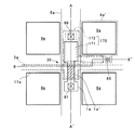
本発明の第1実施形態における電気光学装置の構成について、図1から図4を参照して説明する。図1は、電気光学装置の画像表示領域を構成するマトリクス状に形成された複数の画素における各種素子、配線等の等価回路である。図2は、データ線、走査線、画素電極等が形成されたTFTアレイ基板の相隣接する複数の画素群の平面図である。図3は、図2のA−A’断面図であり、図4は、図2のB−B’断面図である。尚、図3及び図4においては、各層や各部材を図面上で認識可能な程度の大きさとするため、各層や各部材毎に縮尺を異ならしめてある。
【0046】
図1において、本実施形態における電気光学装置の画像表示領域を構成するマトリクス状に形成された複数の画素は、画素電極9aと当該画素電極9aをスイッチング制御するためのTFT30が形成されており、画像信号が供給されるデータ線6aが当該TFT30のソースに電気的に接続されている。データ線6aに書き込む画像信号S1、S2、…、Snは、この順に線順次に供給しても構わないし、相隣接する複数のデータ線6a同士に対して、グループ毎に供給するようにしても良い。また、TFT30のゲートに走査線3aが電気的に接続されており、所定のタイミングで、走査線3aにパルス的に走査信号G1、G2、…、Gmを、この順に線順次で印加するように構成されている。画素電極9aは、TFT30のドレインに電気的に接続されており、スイッチング素子であるTFT30を一定期間だけそのスイッチを閉じることにより、データ線6aから供給される画像信号S1、S2、…、Snを所定のタイミングで書き込む。画素電極9aを介して電気光学物質の一例としての液晶に書き込まれた所定レベルの画像信号S1、S2、…、Snは、対向基板(後述する)に形成された対向電極(後述する)との間で一定期間保持される。液晶は、印加される電圧レベルにより分子集合の配向や秩序が変化することにより、光を変調し、階調表示を可能にする。ノーマリーホワイトモードであれば、各画素の単位で印加された電圧に応じて入射光に対する透過率が減少し、ノーマリーブラックモードであれば、各画素の単位で印加された電圧に応じて入射光に対する透過率が増加され、全体として電気光学装置からは画像信号に応じたコントラストを持つ光が出射する。ここで、保持された画像信号がリークするのを防ぐために、画素電極9aと対向電極との間に形成される液晶容量と並列に蓄積容量70を付加する。
【0047】
本実施形態では特に、蓄積容量70は、TFT30のドレイン(及び画素電極9a)に接続された画素電位側容量電極71と、後述の如く遮光膜からなる固定電位配線の一例たる容量線300に接続された固定電位側容量電極72とが、誘電体膜を介して対向配置されることにより形成されている。そして、画素電位側容量電極71及び固定電位側容量電極72のうちいずれか一方は、後述の如くTFT30を構成する半導体層のチャネル領域を覆うカバー層と同一シリコン層から形成されている。
【0048】
図2において、電気光学装置のTFTアレイ基板上には、マトリクス状に複数の透明な画素電極9a(点線部9a’により輪郭が示されている)が設けられており、画素電極9aの縦横の境界に各々沿ってデータ線6a、走査線3aが設けられている。
【0049】
また、半導体層1aのうち図中右上がりの斜線領域で示したチャネル領域1a’に対向するように走査線3aが配置されており、走査線3aはゲート電極として機能する(特に、本実施形態では、走査線3aは、当該ゲート電極となる部分において幅広に形成されている)。このように、走査線3aとデータ線6aとの交差する個所には夫々、チャネル領域1a’に走査線3aがゲート電極として対向配置された画素スイッチング用のTFT30が設けられている。尚、図2では、4つの画素の内、右上の画素についてのみ、TFT30、蓄積容量70等を詳細に図示しているが、実際にはこれと同様に各画素にTFT30、蓄積容量70等が作り込まれている。
【0050】
本実施形態では、図1に示した容量線300を構成する導電性の上層遮光膜90が(後述のように基板上においてTFT30の上層側に)各画素電極の間隙に沿って格子状に設けられており、下層遮光膜11aも(後述のように基板上においてTFT30の下層側に)同様に格子状に設けられている。これらの上層遮光膜90及び下層遮光膜11aは夫々、例えば、Ti(チタン)、Cr(クロム)、W(タングステン)、Ta(タンタル)、Mo(モリブデン)、Pb(鉛)等の高融点金属のうちの少なくとも一つを含む、金属単体、合金、金属シリサイド、ポリシリサイド、これらを積層したもの等からなる。本実施形態では、特に上層遮光膜90が容量線300としての機能も兼ねるので、これら遮光膜のうち少なくとも上層遮光膜90は導電性材料から形成する必要があるが、下層遮光膜11aが容量線300としての機能を兼ねるように構成するのであれば、逆に少なくとも下層遮光膜11aを導電性材料から形成する必要がある。
【0051】
図2から図4に示すように、本実施形態では特に、TFT30のゲート電極付近の上層側に、シリコン層からなるカバー層80が設けられており、チャネル領域1a’を上側から覆っている。更に走査線3aと同一層から蓄積容量70の画素電位側容量電極71が形成されており、カバー層80と同一シリコン層から蓄積容量70の固定電位側容量電極72が形成されている。これらの画素電位側容量電極71と固定電位側容量電極72とが誘電体膜74を介して対向配置されることにより、平面的に見て主にデータ線6aに重なる領域及び走査線3aに重なる領域に、データ線6a及び走査線3aに沿って伸びる部分を含む略L字型の蓄積容量70が構築されている。また、誘電体膜74は、例えば膜厚5〜200nm程度の比較的薄いHTO膜、LTO膜等の酸化シリコン膜、あるいは窒化シリコン膜等から構成される。蓄積容量70を増大させる観点からは、膜厚の信頼性が十分に得られる限りにおいて、誘電体膜74は薄い程良い。
【0052】
また本実施形態では特に、固定電位側容量電極72をなすシリコン層部分は、不純物がドープされることにより導電性があり、これと同一シリコン層からなるカバー層80をなすシリコン層部分は、不純物がドープされないことにより導電性がない。そして、これらの同一シリコン層からなるカバー層80と固定電位側容量電極72とは、パターン的に分離されていない。
【0053】
図2及び図3に示すように、データ線6aは、コンタクトホール81を介して例えばポリシリコン膜からなる半導体層1aのうち高濃度ソース領域1dに電気的に接続されている。
【0054】
また図2及び図4に示すように、固定電位側容量電極72は、図1の容量線300を構成する上層遮光膜90にコンタクトホール84を介して接続されている。
容量線300として機能する上層遮光膜90は、画素電極9aが配置された画像表示領域からその周囲に延設され、定電位源と電気的に接続されて、固定電位とされる。定電位源としては、TFT30を駆動するための走査信号を走査線3aに供給するための走査線駆動回路(後述する)や画像信号をデータ線6aに供給するサンプリング回路を制御するデータ線駆動回路(後述する)に供給される正電源や負電源の定電位源でも良いし、対向基板の対向電極に供給される定電位でも構わない。
【0055】
尚、TFT30の下側に設けられる下層遮光膜11aについても、その電位変動がTFT30に対して悪影響を及ぼすことを避けるために、上層遮光膜90と同様に、画像表示領域からその周囲に延設して定電位源に接続するとよい。
【0056】
更に図2から図4に示すように、画素電極9aは、画素電位側容量電極71を中継することにより、コンタクトホール83及び85を介して半導体層1aのうち高濃度ドレイン領域1eに電気的に接続されている。
【0057】
尚、図3においてコンタクトホール81は、比較的その深度が深いので、中間にある他の導電層(例えば、画素電位側容量電極71と同一層、固定電位側容量電極72と同一層、上層遮光膜90と同一層)を中継層として利用して、2つ以上の直列なコンタクトホールから構成してもよい。同様に図4においてコンタクトホール85は、比較的その深度が深いので、中間にある他の導電層(例えば、固定電位側容量電極72と同一層、上層遮光膜90と同一層、データ線6aと同一層)を中継層として利用して、2つ以上の直列なコンタクトホールから構成してもよい。このように中間にある他の導電層を中継層として利用すれば、例えば層間距離が例えば1000nm程度に長くても、両者間を一つのコンタクトホールで接続する技術的困難性を回避しつつ比較的小径の二つ以上の直列なコンタクトホールで両者間を良好に接続でき、画素開口率を高めること可能となり、コンタクトホール開孔時におけるエッチングの突き抜け防止にも役立つ。加えて、このように深度の深いコンタクトホール81や85については、エッチングの深度制御の困難性に鑑み、エッチング突き抜け防止用の膜を半導体層1aの下側(コンタクトホール81の場合)や画素電位側容量電極71の下側(コンタクトホール85の場合)に、島状に設けるようにしてもいよい。
【0058】
図3及び4に示すように、電気光学装置は、透明なTFTアレイ基板10と、これに対向配置される透明な対向基板20とを備えている。TFTアレイ基板10は、例えば石英基板、ガラス基板、シリコン基板からなり、対向基板20は、例えばガラス基板や石英基板からなる。TFTアレイ基板10には、画素電極9aが設けられており、その上側には、ラビング処理等の所定の配向処理が施された配向膜16が設けられている。画素電極9aは例えば、ITO(Indium Tin Oxide)膜などの透明導電性薄膜からなる。また配向膜16は例えば、ポリイミド薄膜などの有機薄膜からなる。
【0059】
他方、対向基板20には、その全面に渡って対向電極21が設けられており、その下側には、ラビング処理等の所定の配向処理が施された配向膜22が設けられている。対向電極21は例えば、ITO膜などの透明導電性薄膜からなる。また配向膜22は、ポリイミド薄膜などの有機薄膜からなる。
【0060】
対向基板20には、更に図3及び図4に示すように、格子状又はストライプ状の第2遮光膜23を設けるようにしてもよい。このような構成を採ることで、上層遮光膜90と共に、対向基板20側から入射光がチャネル領域1a’や低濃度ソース領域1b及び低濃度ドレイン領域1cに侵入するのを確実に阻止する。更に、第2遮光膜23は、少なくとも入射光が照射される面を高反射な膜で形成することにより、電気光学装置の温度上昇を防ぐ働きをする。加えて、本実施形態では、Al膜等からなる遮光性のデータ線6aで、各画素の遮光領域のうちデータ線6aに沿った部分を遮光してもよい。
【0061】
このように構成された、画素電極9aと対向電極21とが対面するように配置されたTFTアレイ基板10と対向基板20との間には、後述のシール材により囲まれた空間に電気光学物質の一例である液晶が封入され、液晶層50が形成される。液晶層50は、画素電極9aからの電界が印加されていない状態で配向膜16及び22により所定の配向状態をとる。液晶層50は、例えば一種又は数種類のネマティック液晶を混合した液晶からなる。シール材は、TFTアレイ基板10及び対向基板20をそれらの周辺で貼り合わせるための、例えば光硬化性樹脂や熱硬化性樹脂からなる接着剤であり、両基板間の距離を所定値とするためのグラスファイバー或いはガラスビーズ等のギャップ材が混入されている。
【0062】
更に、画素スイッチング用TFT30の下には、下地絶縁膜12が設けられている。下地絶縁膜12は、TFTアレイ基板10の全面に形成されることにより、TFTアレイ基板10の表面の研磨時における荒れや、洗浄後に残る汚れ等で画素スイッチング用TFT30の特性の劣化を防止する機能を有する。
【0063】
図3において、画素スイッチング用TFT30は、LDD(Lightly Doped Drain)構造を有しており、走査線3a、当該走査線3aからの電界によりチャネルが形成される半導体層1aのチャネル領域1a’、走査線3aと半導体層1aとを絶縁するゲート絶縁膜を含む絶縁薄膜2、半導体層1aの低濃度ソース領域1b及び低濃度ドレイン領域1c、半導体層1aの高濃度ソース領域1d並びに高濃度ドレイン領域1eを備えている。
【0064】
固定電位側容量電極72上には、高濃度ソース領域1dへ通じるコンタクトホール81、固定電位側容量電極72へ通じるコンタクトホール84及び画素電位側容量電極71へ通じるコンタクトホール85が各々開孔された第1層間絶縁膜41が形成されている。
【0065】
第1層間絶縁膜41上には上層遮光膜90が形成されており、これらの上には、高濃度ソース領域1dへ通じるコンタクトホール81及び画素電位側容量電極71へ通じるコンタクトホール85が各々開孔された第2層間絶縁膜42が形成されている。
【0066】
第2層間絶縁膜42上にはデータ線6aが形成されており、これらの上には、画素電位側容量電極71へ通じるコンタクトホール85が形成された第3層間絶縁膜43が形成されている。画素電極9aは、このように構成された第3層間絶縁膜43の上面に設けられている。
【0067】
以上のように構成された本実施形態によれば、対向基板20側からTFT30のチャネル領域1a’及びその付近に入射光が入射しようとすると、第2遮光膜23、データ線6a及び上層遮光膜90で遮光を行う。他方、TFTアレイ基板10側から、TFT30のチャネル領域1a’及びその付近に戻り光が入射しようとすると、下層遮光膜11aで遮光を行う(特に、複板式のカラー表示用のプロジェクタ等で複数の電気光学装置をプリズム等を介して組み合わせて一つの光学系を構成する場合には、他の電気光学装置からプリズム等を突き抜けて来る投射光部分からなる戻り光は強力であるので、有効である。)。そして、斜めの入射光、内面反射光、多重反射光などのTFT30から層間距離を隔てて遮光するのでは、遮光効果が薄い光成分については、TFT30に近接して積層されたカバー層80により吸収する。これらの結果、TFT30の特性が光リークにより劣化することは殆ど無くなり、当該電気光学装置では、非常に高い耐光性が得られる。即ち、本実施形態では、ストレス及び容量カップリングに係る問題を引き起こすこと無くカバー層80をTFT30に近接配置可能であるので、当該カバー層80により、耐光性を十分に高められる。
【0068】
しかも本実施形態では特に、前述の如く固定電位側容量電極72をなすシリコン層部分は、不純物がドープされることにより導電性があるドープドシリコンからなり、カバー層80をなすシリコン層部分は、不純物がドープされないことにより導電性がないノンドープトシリコンからなる。このため、カバー層80をTFT30に近接配置しても容量カップリングは、より一層問題とならないので、チャネル領域1a’に対してカバー層80を、より一層近接配置できるので大変有利である。
【0069】
このようなカバー層の膜厚を、100nm〜300nm、好ましくは200nm程度とすることにより、その光吸収率を実用上十分に高められる。同時にカバー層80の存在により発生するストレスも実用上殆ど問題とならず更にカバー層80の存在に起因して発生する画素電極9aの下地面(第3層間絶縁膜43の表面)における段差も実用上殆ど問題とならない。また、固定電位側容量電極72としても、この程度の膜厚があれば支障はない。そして、より具体的な膜厚については、装置仕様に応じて求められる透過率(光吸収率)、段差、ストレス等の影響を総合的に勘案して設定すればよい。
【0070】
更に本実施形態によれば、カバー層80と同一シリコン層から固定電位側容量電極72が形成された蓄積容量70により、データ線6a及びTFT30を介して画素電極9aに書き込まれた電位を比較的長時間に渡って保持できる。即ち、専ら蓄積容量70の電極としてのみ用いられる導電層を追加的に積層することによる積層構造の複雑化或いは肥大化を避けつつ、限られたTFTアレイ基板10上の領域内に効率的に蓄積容量70を作り込める。
【0071】
本実施形態では特に、固定電位側容量電極72は、TFT30の上層側に積層された上層遮光膜90に接続されることにより、固定電位に落とされているので、基板上で平面的に見て半導体層1aが存在する個所でも、上層遮光膜90と固定電位側容量電極72との間のコンタクトをとれる(即ち、コンタクトホール84を避けるために、平面的に見て半導体層1aを括れさせたり小さくする必要はない)。更にこのようにTFT30の上層側に積層された上層遮光膜90を容量線300(図1参照)として利用することにより、後述する当該電気光学装置の製造プロセスにおいて、蓄積容量70の誘電体膜74を形成後に直ちに(即ち、下側にある固定電位配線に接続するためのコンタクトホールを開孔する作業を挟むこと無く)、カバー層80及び固定電位側容量電極72となるシリコン層を積めるという利益も得られる。
【0072】
加えて本実施形態では特に、同一シリコン層からなるカバー層80と固定電位側容量電極72とはパターン的に分離されていないため、これらをパターン的に分離することによる積層構造の複雑化や装置の信頼性低下を招かなくて済むと同時に、分離する場合と比較して蓄積容量70の構築面積を広げられるため、蓄積容量70の増加を図れる。
【0073】
以上説明した実施形態では、多数の導電層を積層することにより、画素電極9aの下地面(即ち、第3層間絶縁膜43の表面)におけるデータ線6aや走査線3aに沿った領域に段差が生じるが、TFTアレイ基板10、下地絶縁膜12、第1層間絶縁膜41、第2層間絶縁膜42、第3層間絶縁膜43に溝を掘って、データ線6a等の配線やTFT30等を埋め込むことにより平坦化処理を行ってもよいし、第3層間絶縁膜43や第2層間絶縁膜42の上面の段差をCMP(Chemical Mechanical Polishing)処理等で研磨することにより、或いは有機SOGを用いて平らに形成することにより、当該平坦化処理を行ってもよい。
【0074】
更に以上説明した実施形態では、画素スイッチング用TFT30は、好ましくは図3に示したようにLDD構造を持つが、低濃度ソース領域1b及び低濃度ドレイン領域1cに不純物の打ち込みを行わないオフセット構造を持ってよいし、走査線3aの一部からなるゲート電極をマスクとして高濃度で不純物を打ち込み、自己整合的に高濃度ソース及びドレイン領域を形成するセルフアライン型のTFTであってもよい。また本実施形態では、画素スイッチング用TFT30のゲート電極を高濃度ソース領域1d及び高濃度ドレイン領域1e間に1個のみ配置したシングルゲート構造としたが、これらの間に2個以上のゲート電極を配置してもよい。このようにデュアルゲート或いはトリプルゲート以上でTFTを構成すれば、チャネルとソース及びドレイン領域との接合部のリーク電流を防止でき、オフ時の電流を低減することができる。
【0075】
(製造プロセス)
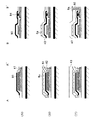
次に、上述の如き構成を持つ第1実施形態における電気光学装置の製造プロセスについて、図5及び図6を参照して説明する。ここに図5及び図6は、第1実施形態の電気光学装置の製造プロセスにおける各工程におけるTFTアレイ基板側の各層を、図4及び図5と同様に図2のA−A’断面及びB−B’断面に対応させて示す工程図である。
【0076】
先ず図5の工程(1)に示すように、石英基板、ハードガラス、シリコン基板等のTFTアレイ基板10を用意する。ここで、好ましくはN2(窒素)等の不活性ガス雰囲気且つ約900〜1300℃の高温でアニール処理し、後に実施される高温プロセスにおけるTFTアレイ基板10に生じる歪みが少なくなるように前処理しておく。そして、このように処理されたTFTアレイ基板10の全面に、Ti、Cr、W、Ta、Mo及びPd等の金属や金属シリサイド等の金属合金膜を、スパッタリングにより、100〜500nm程度の膜厚、好ましくは約200nmの膜厚の遮光膜を形成する。そしてフォトリソグラフィ及びエッチングにより、図2に示した如き所定パターンの下層遮光膜11aを形成する。
【0077】
続いて、下層遮光膜11a上に、例えば、常圧又は減圧CVD法等によりTEOS(テトラ・エチル・オルソ・シリケート)ガス、TEB(テトラ・エチル・ボートレート)ガス、TMOP(テトラ・メチル・オキシ・フォスレート)ガス等を用いて、NSG、PSG、BSG、BPSGなどのシリケートガラス膜、窒化シリコン膜や酸化シリコン膜等からなる下地絶縁膜12を形成する。この下地絶縁膜12の膜厚は、例えば約500〜2000nmとする。
【0078】
続いて、下地絶縁膜12上に、約450〜550℃、好ましくは約500℃の比較的低温環境中で、流量約400〜600cc/minのモノシランガス、ジシランガス等を用いた減圧CVD(例えば、圧力約20〜40PaのCVD)により、アモルファスシリコン膜を形成する。その後、窒素雰囲気中で、約600〜700℃にて約1〜10時間、好ましくは、4〜6時間のアニール処理を施することにより、ポリシリコン膜1を約50〜200nmの厚さ、好ましくは約100nmの厚さとなるまで固相成長させる。固相成長させる方法としては、RTA(Rapid Thermal Anneal)を使ったアニール処理でも良いし、エキシマレーザー等を用いたレーザーアニールでも良い。この際、画素スイッチング用のTFT30を、nチャネル型とするかpチャネル型にするかに応じて、V族元素やIII族元素のドーパントを僅かにイオン注入等によりドープしても良い。そして、フォトリソグラフィ及びエッチングにより、図2に示した如き所定パターンを有する半導体層1aを形成する。
【0079】
次に工程(2)に示すように、TFT30を構成する半導体層1aを約900〜1300℃の温度、好ましくは約1000℃の温度により熱酸化することにより、又は減圧CVD法等により、若しくは両者を続けて行うことにより、単層又は多層の高温酸化シリコン膜(HTO膜)や窒化シリコン膜からなる(ゲート絶縁膜を含む)絶縁薄膜2を形成する。この結果、半導体層1aの厚さは、約30〜150nmの厚さ、好ましくは約35〜50nmの厚さとなり、絶縁薄膜2の厚さは、約20〜150nmの厚さ、好ましくは約30〜100nmの厚さとなる。
【0080】
続いて、絶縁薄膜2に対する反応性イオンエッチング、反応性イオンビームエッチング等のドライエッチングにより、コンタクトホール83を開孔する。更に、減圧CVD法等によりポリシリコン膜を堆積し、更にリン(P)を熱拡散し、このポリシリコン膜を導電化する。又は、Pイオンをこのポリシリコン膜の成膜と同時に導入したドープトシリコン膜を用いてもよい。このポリシリコン膜の膜厚は、約100〜500nmの厚さ、好ましくは約300nmである。そして、フォトリソグラフィ及びエッチングにより、図2に示した如き所定パターンの走査線3aと画素電位側容量電極71とを同時形成する。
【0081】
続いてTFT30をLDD構造を持つnチャネル型のTFTとする場合、半導体層1aに、先ず低濃度ソース領域1b及び低濃度ドレイン領域1cを形成するために、走査線3a(ゲート電極)をマスクとして、PなどのV族元素のドーパントを低濃度で(例えば、Pイオンを1〜3×10¹³/cm2のドーズ量にて)ドープする。これにより走査線3a下の半導体層1aはチャネル領域1a’となる。この不純物のドープにより画素電位側容量電極71及び走査線3aも低抵抗化される。更に、画素スイッチング用TFT30を構成する高濃度ソース領域1d及び高濃度ドレイン領域1eを形成するために、走査線3aよりも幅の広いマスクでレジスト層600を走査線3a上に形成した後、同じくPなどのV族元素のドーパントを高濃度で(例えば、Pイオンを1〜3×1015/cm2のドーズ量にて)ドープする。また、画素スイッチング用TFT30をpチャネル型とする場合、半導体層1aに、低濃度ソース領域1b及び低濃度ドレイン領域1c並びに高濃度ソース領域1d及び高濃度ドレイン領域1eを形成するために、BなどのIII族元素のドーパントを用いてドープする。尚、例えば、低濃度のドープを行わずに、オフセット構造のTFTとしてもよく、走査線3aをマスクとして、Pイオン、Bイオン等を用いたイオン注入技術によりセルフアライン型のTFTとしてもよい。この不純物のドープにより画素電位側容量電極71及び走査線3aも更に低抵抗化される。
【0082】
尚、これらのTFT30の素子形成工程と並行して、nチャネル型TFT及びpチャネル型TFTから構成される相補型構造を持つデータ線駆動回路、走査線駆動回路等の周辺回路をTFTアレイ基板10上の周辺部に形成してもよい。
【0083】
次に工程(3)に示すように、画素電位側容量電極71及び走査線3a並びに絶縁薄膜2上に、減圧CVD法、プラズマCVD法等により高温酸化シリコン膜(HTO膜)や窒化シリコン膜からなる誘電体膜74を25nm以上50nm以下の比較的薄い厚さに堆積する。但し、誘電体膜74は、絶縁薄膜2の場合と同様に、単層膜或いは多層膜のいずれから構成してもよく、一般にTFTのゲート絶縁膜を形成するのに用いられる各種の公知技術により形成可能である。そして、誘電体膜74を薄くする程、蓄積容量70は大きくなるので、結局、膜破れなどの欠陥が生じないことを条件に、膜厚50nm以下の極薄い絶縁膜となるように誘電体膜74を形成すると本実施形態の効果を増大させることができる。
【0084】
続いて、誘電体膜74上に導電性のないポリシリコン層を減圧CVD法等により堆積した後、フォトリソグラフィ及びエッチングにより、図2に示した如きカバー層80及び固定電位側容量電極72’(導電性が付与される前の電極)を含む所定パターンのシリコン層とする。この際のシリコン層の膜厚としては、100nm以上300nm以下程度が好ましいが、前述の如く装置仕様に応じて求められる透過率(光吸収率)、段差、ストレス等の影響を総合的に勘案して設定する。
【0085】
次に、工程(4)では、フォトリソグラフィ及びエッチングにより、カバー層80となるシリコン層部分をマスクするレジスト601を形成した後に、矢印600で示した方向からイオン打ち込みを行って、固定電位側容量電極72’を低抵抗化する。即ち、ドープトシリコンからなる固定電位側容量電極72が完成する。この際、カバー層80についてはドープされない。即ち、カバー層80は、ノンドープトシリコンからなる。
【0086】
次に、図6の工程(5)に示すように、レジスト500を除去した後に、例えば、常圧又は減圧CVD法やTEOSガス等を用いて、NSG、PSG、BSG、BPSGなどのシリケートガラス膜、窒化シリコン膜や酸化シリコン膜等からなる第1層間絶縁膜41を形成する。第1層間絶縁膜41の膜厚は、例えば500〜1500nm程度である。
【0087】
更に、第1層間絶縁膜41に対する反応性イオンエッチング、反応性イオンビームエッチング等のドライエッチングにより、コンタクトホール84を開孔する。その後、第1層間絶縁膜41上の全面に、Ti、Cr、W、Ta、Mo及びPd等の金属や金属シリサイド等の金属合金膜を、スパッタリングにより例えば100〜500nm程度の膜厚に形成した後に、フォトリソグラフィ及びエッチングを行って、図2に示した如き所定パターンを有する上層遮光膜90を形成する。
【0088】
次に、工程(6)では、上層遮光膜90上に、例えば、常圧又は減圧CVD法やTEOSガス等を用いて、NSG、PSG、BSG、BPSGなどのシリケートガラス膜、窒化シリコン膜や酸化シリコン膜等からなる第2層間絶縁膜42を形成する。第2層間絶縁膜42の膜厚は、例えば500〜1500nm程度である。
【0089】
続いて、第2層間絶縁膜42に対する反応性イオンエッチング、反応性イオンビームエッチング等のドライエッチングにより、コンタクトホール81を開孔する。この際、走査線3aや上層遮光膜90を基板周辺領域において図示しない配線と接続するためのコンタクトホールも、コンタクトホール81と同一の工程により第2層間絶縁膜42に開孔することができる。その後、第1層間絶縁膜41上の全面に、スパッタリング等により、遮光性のAl等の低抵抗金属や金属シリサイド等を金属膜として、約100〜500nmの厚さ、好ましくは約300nmに堆積する。そして、フォトリソグラフィ及びエッチングにより、図2に示した如き所定パターンを有するデータ線6aを形成する。
【0090】
次に工程(7)に示すように、データ線6a上を覆うように、例えば、常圧又は減圧CVD法やTEOSガス等を用いて、NSG、PSG、BSG、BPSGなどのシリケートガラス膜、窒化シリコン膜や酸化シリコン膜等からなる第3層間絶縁膜43を形成する。第3層間絶縁膜43の膜厚は、例えば500〜1500nm程度である。
【0091】
続いて、第3層間絶縁膜43に対する反応性イオンエッチング、反応性イオンビームエッチング等のドライエッチングにより、コンタクトホール85を開孔する。
【0092】
続いて、第3層間絶縁膜43上に、スパッタ処理等により、ITO膜等の透明導電性薄膜を、約50〜200nmの厚さに堆積する。そして、フォトリソグラフィ及びエッチングにより、図2に示した如き所定パターンを有する画素電極9aを形成する。尚、当該液晶装置を反射型の液晶装置に用いる場合には、Al等の反射率の高い不透明な材料から画素電極9aを形成してもよい。
【0093】
続いて、画素電極9aの上にポリイミド系の配向膜の塗布液を塗布した後、所定のプレティルト角を持つように且つ所定方向でラビング処理を施すこと等により、配向膜16(図3及び図4参照)が形成される。
【0094】
他方、図3及び図4に示した対向基板20については、ガラス基板等が先ず用意され、第2遮光膜23及び額縁としての遮光膜(図14及び図15参照)が、例えば金属クロムをスパッタした後、フォトリソグラフィ及びエッチングを経て形成される。尚、これらの遮光膜は、導電性である必要はなく、Cr、Ni、Alなどの金属材料の他、カーボンやTiをフォトレジストに分散した樹脂ブラックなどの材料から形成してもよい。尚、TFTアレイ基板10上で、データ線6a、カバー層80、下層遮光膜11a等で遮光領域を規定すれば、対向基板20上の第2遮光膜23を省くことができる。
【0095】
その後、対向基板20の全面にスパッタ処理等により、ITO等の透明導電性薄膜を、約50〜200nmの厚さに堆積することにより、対向電極21を形成する。更に、対向電極21の全面にポリイミド系の配向膜の塗布液を塗布した後、所定のプレティルト角を持つように且つ所定方向でラビング処理を施すこと等により、配向膜22(図3及び図4参照)が形成される。
【0096】
最後に、上述のように各層が形成されたTFTアレイ基板10と対向基板20とは、配向膜16及び22が対面するようにシール材(図14及び図15参照)により貼り合わされ、真空吸引等により、両基板間の空間に、例えば複数種類のネマティック液晶を混合してなる液晶が吸引されて、所定層厚の液晶層50が形成される。
【0097】
以上説明したように本製造プロセスでは、図5の工程(3)及び(4)で、同一シリコン層から、カバー層80及び固定電位側容量電極72を形成するので、前述した第1実施形態の電気光学装置を比較的容易に製造できる。特に、工程(4)で、カバー層80をなすシリコン層部分をマスクしてのイオン打ち込みにより、カバー層80に導電性を与えることなく、固定電位側容量電極72をなすシリコン層部分にのみ導電性の与えることができる。これにより、パターン的に分離されていないカバー層80であって、TFT30に近接配置してもTFT30との容量カップリングが問題とならない導電性のないカバー層80を、比較的容易に製造できる。
【0098】
(第2実施形態)
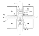
次に、図7から図9を参照して本発明の電気光学装置の第2実施形態について説明する。ここに、図7は、データ線、走査線、画素電極等が形成されたTFTアレイ基板の画素の平面図であり、図8は、図7におけるカバー層を中心とする主な積層構造を示すA−A’断面図であり、図9は、その変形例におけるA−A’断面図である。尚、図8及び図9においては、各層や各部材を図面上で認識可能な程度の大きさとするため、各層や各部材毎に縮尺を適宜異ならしめてある。また、図7から図9において、図1から図3(第1実施形態)と同様の構成要素には、同様の参照符号を付し、その説明は省略する。
【0099】
図7及び図8に示すように、第2実施形態では、第1実施形態と異なり、上層遮光膜90が存在しておらず(更に、これに伴って第2層間絶縁膜42及びコンタクトホール84が存在しておらず)、代りに、カバー層80と同一シリコン層からなる固定電位側容量電極172が、コンタクトホール86を介して下層遮光膜11aに接続されて、固定電位に落とされている。また、走査線3aと同一層からではなく、半導体層1aの高濃度ドレイン領域1aから延設された導電性ポリシリコン膜部分から、画素電位側容量電極171が形成されており、この画素電位側容量電極171と固定電位側容量電極172とが誘電体膜174を介して対向配置されることで蓄積容量170が構築されている。更に、半導体層1aの平面形状については、コンタクトホール86が開孔可能なように、図8における上端付近が若干短くされ、蓄積容量170を増大させるように画素電位側容量電極171をなす部分が、走査線に沿った領域にも(図8中、右側に)延設されている。また、半導体層1aの図8中の右端付近に画素電極9aからのコンタクトホール85が開孔されている。他方、蓄積容量170の誘電体膜を厚くしないように、この領域におけるゲート絶縁膜2を含む絶縁薄膜2がエッチングにより除去されている。その他の構成については、図8で省略されている画素電極9a、対向基板20等の構成を含めて、図2から図4に示した第1実施形態の場合と同様である。
【0100】
従って第2実施形態によれば、各画素の非開口領域を少なくとも部分的に規定する下層遮光膜11aは、遮光機能のみならず図1に示した容量線300としての機能も有する。そして、このような下層遮光膜11aは好ましくは、第1実施形態における上層遮光膜90の場合と同様に、画素電極9aが配置された画像表示領域からその周囲に延設され、定電位源と電気的に接続される。
【0101】
尚、図9に示したように蓄積容量170を、走査線3aに重なる領域にまで(L字型に)作り込むことなく、データ線6aに重なる領域にのみに(矩形に)作り込んでもよい。この場合、走査線3aに沿った画素非開口領域を不必要に広げないように、半導体層1aの高濃度ドレイン領域1eから延設された角状部を画素電極9a下に突出させおき、この部分に画素電極9aからのコンタクトホール185が開孔されている。
【0102】
(第3実施形態)
次に、図10から図12を参照して本発明の電気光学装置の第3実施形態について説明する。ここに、図10は、データ線、走査線、画素電極等が形成されたTFTアレイ基板の画素の平面図であり、図11は、図10におけるカバー層を中心とする主な積層構造を示すA−A’断面図であり、図12は、その変形例におけるA−A’断面図である。尚、図11及び図12においては、各層や各部材を図面上で認識可能な程度の大きさとするため、各層や各部材毎に縮尺を適宜異ならしめてある。また、図10から図13において、図1から図3(第1実施形態)或いは図と同様の構成要素には、同様の参照符号を付し、その説明は省略する。
【0103】
図10及び図11に示すように、第3実施形態では、第2実施形態と比べて、同一シリコン層からなるカバー層80’と固定電位側容量電極172’とが、パターン的に分離されている。その他の構成については、第2実施形態の場合と同様である。
【0104】
従って第3実施形態によれば、各画素の非開口領域を少なくとも部分的に規定する下層遮光膜11aは、遮光機能のみならず図1に示した容量線300としての機能も有する。そして特にカバー層80’と固定電位側容量電極172’とが分離されているため、これらを積層構造内に追加的に作り込むことに起因するストレスの緩和が図れる。更に固定電位側容量電極72における微弱な電位変動がカバー層80を介してTFT30に悪影響を及ぼす事態を防止できる。
【0105】
尚、図12に示したように蓄積容量170を、走査線3aに重なる領域にまで(L字型に)作り込むことなく、データ線6aに重なる領域にのみに(矩形に)作り込んでもよい。この場合、走査線3aに沿った画素非開口領域を不必要に広げないように、半導体層1aの高濃度ドレイン領域1eから延設された角状部を画素電極9a下に突出させおき、この部分に画素電極9aからのコンタクトホール185が開孔されている。
【0106】
以上説明した第2及び第3実施形態では、第1実施形態の場合とは異なり、下層遮光膜11aに図1における容量線300としての機能を与えるが故に、容量線300としての機能を持たない上層遮光膜を省略しているが、第2及び第3実施形態でも、第1実施形態の上層遮光膜90の如き遮光膜を専ら遮光の目的で設けるようにしてもよい。即ち、耐光性を高めるためには、TFT30の上下に上層遮光膜及び下層遮光膜が夫々配置されている方がより好ましい。
【0107】
ここで、図13を参照して本発明の各実施形態の電気光学装置における下層遮光膜と上層遮光膜との形状についての好ましい関係について説明を加える。ここに、図13は、下層遮光膜及び上層遮光膜のみを抽出して示すTFTアレイ基板の画素の平面図である。
【0108】
図13に示すように、各実施形態では、下層遮光膜11a及び上層遮光膜90共に格子状に形成されており、下層遮光膜11aは、平面的に見て上層遮光膜90の形成領域からはみ出さないように(即ち、一回り小さく)構成されている。従って上層遮光膜90により各画素の開口領域の輪郭が規定される。また、両者間にある不図示の走査線、データ線及びTFT等は、平面的に見て下層遮光膜11aの形成領域からはみ出さないように構成されている。
【0109】
従って、対向基板20側からの入射光が上層遮光膜90の形成領域からはみ出した下層遮光膜11a(更に、走査線、データ線等)で反射することで、当該電気光学装置の内部における内面反射光や多重反射光が発生することを効果的に未然防止できる。尚、TFTアレイ基板10側からの戻り光が下層遮光膜11aの形成領域からはみ出した上層遮光膜90部分で反射することで、当該電気光学装置の内部における内面反射光や多重反射光は若干発生する。しかしながら、戻り光は入射光に比べて遥かに光強度が低いために、戻り光による内面反射や多重反射光の悪影響は入射光のそれに比べて軽微である。そして、このような軽微な内面反射光や多重反射光であれば、TFT30に近接配置されたシリコン層からなるカバー層80によって十分に吸収可能である。従って本実施形態の構成は有利である。
【0110】
(その他の変形形態)
以上説明した各実施形態では、カバー層80をなすシリコン層部分は、ノンドープトシリコンからなり導電性がないが、カバー層80も、同一シリコン層から形成される固定電位側容量電極72と同様に、不純物がドープされることにより導電性があるドープトシリコンから形成されてもよい。この場合には、カバー層80を固定電位に落とすことにより、TFT30に近接配置しても容量カップリングは殆ど問題とならない。このようにカバー層80を導電性のドープトシリコンから構成する場合には、TFT30との寄生容量を確実に抑制する観点からは、カバー層80とTFT30(即ち、ゲート電極を構成する走査線3a)との間に介在する層間絶縁膜(誘電体膜)の膜厚を400nm以上とするのが好ましい。従って、このような比較的厚い層間絶縁膜を蓄積容量の誘電体膜をとしてそのまま用いることは望ましくない(即ち、誘電体膜の膜厚に反比例して容量が小さくなってしまう)ので、当該層間絶縁膜を誘電体膜となる部分において局所的にエッチングして、25nm〜50nmの薄い誘電体膜にすればよい。尚、このような電気光学装置は、例えば図5の工程(4)において、カバー層80となる部分をマスクすることなく、カバー層80及び固定電位側容量電極72をなすシリコン層に対してイオン打ち込みを行って、低抵抗のドープトシリコン層とすればよい。更に、このようにカバー層80に導電性を持たせる場合には、これと同一シリコン層からなる電極からパターン的に分離して、更に別途コンタクトホールを介して上層遮光膜、下層遮光膜等からなる固定電位配線に接続しても、導電性のあるカバー層80を固定電位に落とせる。特に、カバー層80と同一シリコン層からなる電極を画素電位電極として用いる場合にはこのような構成を採るとよい。
【0111】
以上説明した各実施形態においては、固定電位側容量電極72がカバー層80と同一シリコン膜から形成されているが、画素電位側容量電極71がカバー層80と同一シリコン膜から形成されてもよい。また、以上説明した各実施形態では、カバー層80と同一シリコン層から形成されない方の電極については、導電性のポリシリコン膜からなる走査線3aや半導体層1aと同一層から形成されているが、例えばITO膜からなる画素電極9aと同一層、上層又は下層遮光膜と同一層、データ線と同一層等から形成されてもよい。更に、固定電位側容量電極は、TFT30の上側(例えば、走査線3aと画素電位側容量電極71との間やデータ線6aと画素電位側容量電極71との間)に積層されてもよいし、TFT30の下側に積層されてもよい。但し、容量線300として機能する遮光膜と固定電位側容量電極との層間距離が短いほど両者をコンタクトホール等により接続するのが容易となり積層構造の複雑化を招かないで済むと共に装置信頼性が高まる。
【0112】
加えて、上述した各実施形態は、画素電極等が透明であり入射光を透過する透過型の電気光学装置として構築されているが、画素電極が反射膜であるか或いは反射膜が画素電極下に配置されており入射光を反射する反射型の電気光学装置として構築されてもよい。
【0113】
(電気光学装置の全体構成)
以上のように構成された各実施形態における電気光学装置の全体構成を図14及び図15を参照して説明する。尚、図14は、TFTアレイ基板10をその上に形成された各構成要素と共に対向基板20の側から見た平面図であり、図15は、図14のH−H’断面図である。
【0114】
図15において、TFTアレイ基板10の上には、シール材52がその縁に沿って設けられており、その内側に並行して、例えば第2遮光膜23と同じ或いは異なる材料から成る画像表示領域10aの周辺を規定する額縁としての第3遮光膜53が設けられている。シール材52の外側の領域には、データ線6aに画像信号を所定タイミングで供給することによりデータ線6aを駆動するデータ線駆動回路101及び外部回路接続端子102がTFTアレイ基板10の一辺に沿って設けられており、走査線3aに走査信号を所定タイミングで供給することにより走査線3aを駆動する走査線駆動回路104が、この一辺に隣接する2辺に沿って設けられている。走査線3aに供給される走査信号遅延が問題にならないのならば、走査線駆動回路104は片側だけでも良いことは言うまでもない。また、データ線駆動回路101を画像表示領域10aの辺に沿って両側に配列してもよい。更にTFTアレイ基板10の残る一辺には、画像表示領域10aの両側に設けられた走査線駆動回路104間をつなぐための複数の配線105が設けられている。また、対向基板20のコーナー部の少なくとも1箇所においては、TFTアレイ基板10と対向基板20との間で電気的に導通をとるための導通材106が設けられている。そして、図15に示すように、図14に示したシール材52とほぼ同じ輪郭を持つ対向基板20が当該シール材52によりTFTアレイ基板10に固着されている。
【0115】
尚、TFTアレイ基板10上には、これらのデータ線駆動回路101、走査線駆動回路104等に加えて、複数のデータ線6aに画像信号を所定のタイミングで印加するサンプリング回路、複数のデータ線6aに所定電圧レベルのプリチャージ信号を画像信号に先行して各々供給するプリチャージ回路、製造途中や出荷時の当該電気光学装置の品質、欠陥等を検査するための検査回路等を形成してもよい。
【0116】
以上図1から図15を参照して説明した各実施形態では、データ線駆動回路101及び走査線駆動回路104をTFTアレイ基板10の上に設ける代わりに、例えばTAB(Tape Automated bonding)基板上に実装された駆動用LSIに、TFTアレイ基板10の周辺部に設けられた異方性導電フィルムを介して電気的及び機械的に接続するようにしてもよい。また、対向基板20の投射光が入射する側及びTFTアレイ基板10の出射光が出射する側には各々、例えば、TNモード、VA(Vertically Aligned)モード、PDLC(Polymer Dispersed Liquid Crystal)モード等の動作モードや、ノーマリーホワイトモード/ノーマリーブラックモードの別に応じて、偏光フィルム、位相差フィルム、偏光板などが所定の方向で配置される。
【0117】
以上説明した各実施形態における電気光学装置は、プロジェクタに適用されるため、3枚の電気光学装置がRGB用のライトバルブとして各々用いられ、各ライトバルブには各々RGB色分解用のダイクロイックミラーを介して分解された各色の光が投射光として各々入射されることになる。従って、各実施形態では、対向基板20に、カラーフィルタは設けられていない。しかしながら、第2遮光膜23の形成されていない画素電極9aに対向する所定領域にRGBのカラーフィルタをその保護膜と共に、対向基板20上に形成してもよい。このようにすれば、プロジェクタ以外の直視型や反射型のカラー電気光学装置について、各実施形態における電気光学装置を適用できる。また、対向基板20上に1画素1個対応するようにマイクロレンズを形成してもよい。あるいは、TFTアレイ基板10上のRGBに対向する画素電極9a下にカラーレジスト等でカラーフィルタ層を形成することも可能である。このようにすれば、入射光の集光効率を向上することで、明るい電気光学装置が実現できる。更にまた、対向基板20上に、何層もの屈折率の相違する干渉層を堆積することで、光の干渉を利用して、RGB色を作り出すダイクロイックフィルタを形成してもよい。このダイクロイックフィルタ付き対向基板によれば、より明るいカラー電気光学装置が実現できる。
【0118】
本発明は、上述した各実施形態に限られるものではなく、請求の範囲及び明細書全体から読み取れる発明の要旨或いは思想に反しない範囲で適宜変更可能であり、そのような変更を伴なう電気光学装置及びその製造方法もまた本発明の技術的範囲に含まれるものである。
【図面の簡単な説明】
【図1】本発明の第1実施形態の電気光学装置における画像表示領域を構成するマトリクス状の複数の画素に設けられた各種素子、配線等の等価回路である。
【図2】第1実施形態の電気光学装置におけるデータ線、走査線、画素電極等が形成されたTFTアレイ基板の相隣接する複数の画素群の平面図である。
【図3】図2のA−A’断面図である。
【図4】図2のB−B’断面図である。
【図5】第1実施形態の電気光学装置の製造プロセスにおける各工程におけるTFTアレイ基板側の各層を、図4及び図5と同様に図2のA−A’断面及びB−B’断面に対応させて示す工程図(その1)である。
【図6】第1実施形態の電気光学装置の製造プロセスにおける各工程におけるTFTアレイ基板側の各層を、図4及び図5と同様に図2のA−A’断面及びB−B’断面に対応させて示す工程図(その2)である。
【図7】第2実施形態の電気光学装置におけるデータ線、走査線、画素電極等が形成されたTFTアレイ基板の相隣接する複数の画素群の平面図である。
【図8】第2実施形態におけるカバー層を中心とする主な積層構造を示す図7のA−A’断面図である。
【図9】第2実施形態の変形例における図7のA−A’断面図である。
【図10】第3実施形態の電気光学装置におけるデータ線、走査線、画素電極等が形成されたTFTアレイ基板の相隣接する複数の画素群の平面図である。
【図11】第3実施形態におけるカバー層を中心とする主な積層構造を示す図10のA−A’断面図である。
【図12】第3実施形態の変形例における図10のA−A’断面図である。
【図13】各実施形態における上層遮光膜及び下層遮光膜を抽出して示すTFTアレイ基板の画素の平面図である。
【図14】各実施形態の電気光学装置におけるTFTアレイ基板をその上に形成された各構成要素と共に対向基板の側から見た平面図である。
【図15】図14のH−H’断面図である。
【符号の説明】
1a…半導体層
1a’…チャネル領域
1b…低濃度ソース領域
1c…低濃度ドレイン領域
1d…高濃度ソース領域
1e…高濃度ドレイン領域
2…絶縁薄膜
3a…走査線
6a…データ線
9a…画素電極
10…TFTアレイ基板
11a…下層遮光膜
12…下地絶縁膜
16…配向膜
20…対向基板
21…対向電極
22…配向膜
23…第2遮光膜
30…TFT
50…液晶層
70…蓄積容量
71…画素電位側容量電極
72…固定電位側容量電極
74…誘電体膜
80…カバー層
90…上層遮光膜
81、83、85…コンタクトホール
300…容量線[0001]
BACKGROUND OF THE INVENTION
The present invention belongs to the technical field of an active matrix drive type electro-optical device, and in particular, a storage capacitor for holding a potential written in a pixel electrode, a thin film transistor for pixel switching (hereinafter referred to as a TFT as appropriate). Belongs to the technical field of an electro-optical device of a type provided in a laminated structure on a substrate and a manufacturing method thereof.
[0002]
[Background]
In an electro-optical device of the TFT active matrix driving type, when incident light is irradiated to a channel region of a pixel switching TFT provided in each pixel, a current is generated by excitation by light, and the characteristics of the TFT change. In particular, in the case of an electro-optical device for a projector light valve, since the intensity of incident light is high, it is important to shield incident light from the TFT channel region and its peripheral region. Therefore, conventionally, the channel region and its peripheral region are shielded by a light shielding film that defines the opening region of each pixel provided on the counter substrate, or by a data line that passes over the TFT and is made of a metal film such as Al. Is configured to do. Japanese Patent Laid-Open No. 9-33944 discloses a technique for reducing light incident on a channel region with a light shielding film formed of a-Si (amorphous silicon) having a large refractive index. Furthermore, a light shielding film made of, for example, a refractory metal may be provided at a position facing the pixel switching TFT on the TFT array substrate (that is, below the TFT). If a light-shielding film is also provided on the lower side of the TFT in this way, the back surface reflection from the TFT array substrate side, or when combining a plurality of electro-optical devices via a prism or the like, Projection light penetrating through the prism or the like from the electro-optical device can be prevented from entering the TFT of the electro-optical device.
[0003]
On the other hand, generally in this type of electro-optical device, when a scanning signal is supplied to the gate electrode of the TFT via the scanning line, the TFT is turned on and supplied to the source region of the semiconductor layer via the data line. An image signal is supplied to the pixel electrode through the source and drain of the TFT. Since such an image signal is supplied only for a very short time for each pixel electrode through each TFT, the voltage of the image signal supplied through the TFT is set to be much longer than the time in which it is turned on. In general, a storage capacitor is added to each pixel electrode (in parallel with a liquid crystal capacitor or the like) so that the pixel electrode can be held for a long time. Such a storage capacitor generally has a capacitor electrode extending from a conductive polysilicon film or the like constituting a drain region of a TFT connected to the pixel electrode and having a pixel electrode potential, and a dielectric material on the capacitor electrode. A capacitor line including an electrode portion arranged opposite to each other through a film and having a fixed potential is configured.
[0004]
[Problems to be solved by the invention]
However, the various light shielding techniques described above have the following problems. That is, according to the technique of forming a light shielding film on the counter substrate or the TFT array substrate, the space between the light shielding film and the channel region is, for example, through a liquid crystal layer, an electrode, an interlayer insulating film, etc. in three dimensions. The light is obliquely separated from each other, and the light is not sufficiently shielded. In addition, after the light that has entered the electro-optical device from the region without the light shielding film is reflected by the inner surface of the light shielding film or the data line (that is, the surface facing the channel region), the reflected light or In some cases, the multiple reflected light reflected from the inner surface of the light shielding film or the data line finally reaches the channel region of the TFT. In addition, according to the technology for shielding light by the data line, the data line is formed in a stripe shape extending in a direction perpendicular to the scanning line when seen in a plan view, and the adverse effect of capacitive coupling between the data line and the channel region is negligible. Since it is necessary to dispose a thick interlayer insulating film between the two, it is basically difficult to sufficiently shield the light. Further, according to the technique described in Japanese Patent Application Laid-Open No. 9-33944, an a-Si film is formed on the gate line, so that the adverse effect of capacitive coupling between the gate electrode and the a-Si film is reduced. It is necessary to stack a relatively thick interlayer insulating film. As a result, the a-Si film, the interlayer insulating film, and the like that are additionally formed increase the complexity of the laminated structure, and it is also difficult to sufficiently shield oblique incident light and inner surface reflected light. In particular, according to various conventional light-shielding techniques described above, sufficient light shielding can be achieved as the electro-optical device is refined or the pixel pitch is made finer in order to meet the general demand for high-quality display images in recent years. It becomes more difficult to apply, and there is a problem that the flicker or the like occurs due to a change in the transistor characteristics of the TFT and the quality of the display image is lowered.
[0005]
On the other hand, the above-described technology for adding a storage capacity has the following problems. In other words, in this type of electro-optical device, the pixel aperture ratio is increased while reducing the pixel pitch in order to improve the display image quality (that is, in each pixel, in the non-aperture region in each pixel through which display light is not transmitted). On the other hand, it is important to widen the opening area through which the display light is transmitted), but the non-opening area of each pixel to which the scanning line and the capacitor line can be routed as the aperture ratio of the fine pitch pixel increases as described above. Narrow. For this reason, as the pixel pitch becomes finer, it becomes more difficult to create a sufficiently large storage capacitor and to provide sufficient conductivity to the scanning line and the capacitor line. If sufficient storage capacity cannot be obtained or sufficient conductivity is not obtained for the scanning lines and the capacity lines, eventually, crosstalk and ghosts in the display image increase and image quality deteriorates. Problems arise.
[0006]
The present invention has been made in view of the above-described problems, and an object thereof is to provide an electro-optical device that is excellent in light resistance and can efficiently build a storage capacitor, and a method for manufacturing the same.
[0007]
[Means for Solving the Problems]
In order to solve the above problems, an electro-optical device according to an aspect of the invention includes a scanning line and a data line intersecting with each other on a substrate, a thin film transistor connected to the scanning line and the data line, and a pixel electrode connected to the thin film transistor. And a pixel potential side capacitor electrode connected to the pixel electrode to be a pixel electrode potential, and a fixed potential side capacitor electrode which is disposed opposite to the pixel potential side capacitor electrode through a dielectric film and is set to a fixed potential. A capacitor and a cover layer stacked at a position covering at least the channel region of the semiconductor layer constituting the thin film transistor in plan view, and one of the pixel potential side capacitor electrode and the fixed potential side capacitor electrode The electrode and the cover layer are formed of the same silicon layer.
[0008]
According to the electro-optical device of the present invention, the thin film transistor is planarized by a cover layer made of various silicon layers such as p-Si (polysilicon film), a-Si (amorphous silicon film), doped silicon, and non-doped silicon. Covered (ie, from the top or bottom on the substrate). Such a silicon layer is generally brownish, and has a higher light absorption rate (ie, transmittance) than glass materials such as PSG (phosphorus silicate glass) and BSG (boron silicate glass) that constitute the interlayer insulating film. Is low) and absorbs light. In the case of a silicon layer, unlike the case where light is shielded by a metal layer such as Ti (titanium) or Cr (chromium), the stress generated between the semiconductor layer and the gate electrode layer constituting the thin film transistor can be reduced. It can be arranged as close as possible to the thin film transistor. That is, even when a cover layer made of the silicon layer is disposed on a thin film transistor via a thin interlayer insulating film, stress generated during manufacturing or after completion of the product hardly poses a problem. In particular, when the light intensity is increased, even in the case of such a light-shielding metal layer, it is necessary to make it thicker. The resulting cover layer is very advantageous. Furthermore, the cover layer and the thin film transistor (especially its gate electrode and semiconductor) are formed by forming the cover layer from a non-doped silicon layer having no conductivity, or from a silicon layer having conductivity and dropping it to a fixed potential. Even if the layers are arranged close to each other, there is almost no problem with capacitive coupling between them. Therefore, according to the present invention, light (for example, oblique incident light, internal reflection light, multiple reflection) that is intended to be incident on the channel region is provided by a cover layer that can be disposed close to each other without causing problems related to stress and capacitive coupling. Light, return light from the back surface, etc.) can be shielded near the channel region. For this reason, according to the present invention, the obliquely incident light or the like cannot be sufficiently shielded by the light shielding film disposed relatively far as in the background art described above, which is very advantageous.
[0009]
In addition, according to the present invention, the potential written to the pixel electrode via the data line and the thin film transistor over a relatively long time is caused by the storage capacitor in which one electrode is formed from the same silicon layer as the cover layer. Can be held. That is, the storage capacitor can be constructed while avoiding complication or enlargement of the stacked structure by additionally stacking conductive layers that are used exclusively as electrodes of the storage capacitor. At this time, if one of the electrodes is a fixed potential side capacitance electrode, the cover layer is formed regardless of whether the silicon layer portion forming the cover layer is non-conductive silicon or non-conductive silicon. It is not necessary to separate and pattern the layer and one electrode. If one of the electrodes is a pixel potential side capacitive electrode, the silicon layer portion forming the cover layer may be a non-conductive silicon layer having no conductivity (in this case, the potential of the cover layer may be a floating potential). . Alternatively, the silicon layer portion forming the cover layer may be a conductive doped silicon layer, and the cover layer and one electrode may be separated and patterned. In this case, the cover layer is preferably set to a fixed potential. Drop it. The fixed potential may be a ground potential or a counter electrode potential. In any case, it is preferable that the cover layer is made conductive and dropped to a fixed potential or not made conductive so that the cover layer can be disposed close to the channel region. As described above, according to the present invention, the same silicon layer as the cover layer can be used as one electrode of the storage capacitor while satisfying desirable conditions for light absorption in the cover layer, so that the laminated structure as a whole becomes complicated or enlarged. Thus, it is possible to efficiently create a storage capacity in a limited area on the substrate.
[0010]
As a result of the above, according to the present invention, it is possible to efficiently build a storage capacitor with excellent light resistance. Flicker is caused by a change in transistor characteristics of a thin film transistor due to particularly excellent light resistance, and the quality of a display image is improved. It is possible to improve the image quality by reducing crosstalk and ghosting in the displayed image while avoiding the problem of lowering and simultaneously increasing the aperture ratio of pixels with fine pitches by the storage capacity that is efficiently created at the same time. .
[0011]
Note that such a thin film transistor may be a so-called top gate type in which a gate electrode formed of a part of a scanning line is positioned above the channel region, or a gate electrode formed of a part of the scanning line is formed below the channel region. A so-called bottom gate type may be used. The interlayer position of the storage capacitor may be above or below the scanning line on the substrate. In addition, the interlayer position of the pixel electrode may be above or below the scanning line on the substrate. Further, the cover layer may be stacked on the upper side or the lower side of the thin film transistor. Furthermore, the vertical relationship on the substrate of the pixel potential side capacitance electrode and the fixed potential side capacitance electrode may be either, and the other electrode is a conductive layer such as a semiconductor layer, a scanning line, a data line, a light shielding film, or a pixel electrode. Can be composed of the same film. In addition, the electro-optical device of the present invention configured as described above may be a transmissive electro-optical device or a reflective electro-optical device.
[0012]
In one aspect of the electro-optical device of the present invention, the cover layer has a thickness of 100 nm to 300 nm.
[0013]
According to this aspect, by setting the film thickness of the cover layer to 100 nm to 300 nm, preferably about 200 nm, the light absorption rate can be sufficiently increased in practical use. In addition, with such a film thickness, the stress generated by the presence of the cover layer is hardly a problem in practice, and further, the step on the ground of the pixel electrode caused by the presence of the cover layer is also practical. It is suppressed to the extent that it hardly causes a problem.
[0014]
In another aspect of the electro-optical device of the present invention, the silicon layer portion forming the one electrode is conductive by being doped with impurities, and the silicon layer portion forming the cover layer is not doped with the impurities. Therefore, the conductivity is smaller than that of the one electrode.
[0015]
According to this aspect, one of the electrodes is electrically conductive by being doped with impurities (that is, made of doped silicon), and therefore can function well as an electrode of a storage capacitor. On the other hand, the cover layer has low conductivity because it is not doped with impurities (that is, made of non-doped silicon). For this reason, even if the cover layer is arranged close to the thin film transistor (particularly its gate electrode or semiconductor layer), the capacitive coupling hardly causes a problem. Therefore, the cover layer arranged close to the channel region tends to enter the channel region. Oblique incident light and the like can be absorbed. In particular, according to the present aspect in which the conductive cover layer and one electrode are separated in a pattern, the reliability is obtained according to the present embodiment in which both are separated depending on the presence or absence of doping.
[0016]
In an aspect in which the conductivity of the cover layer is small, the cover layer may not be separated from the one electrode in a pattern.
[0017]
That is, with this configuration, the cover layer (made of non-doped silicon) has low conductivity even if it is not separated from one electrode in a pattern, so that one electrode is a pixel potential side capacitor electrode. However, the potential of the cover layer does not fluctuate according to the pixel electrode potential. Therefore, the potential fluctuation of the cover layer hardly affects the channel region. Alternatively, if one of the electrodes is a fixed potential side capacitance electrode, the potential fluctuation of the cover layer hardly affects the channel region. Therefore, it is not necessary to complicate the laminated structure and reduce the reliability of the device by pattern-separating the cover layer made of the same silicon layer and the one electrode. At the same time, the area of one electrode of the storage capacitor can be increased compared to the case of separation, so that the storage capacitor can be increased.
[0018]
Alternatively, in another aspect of the present invention, the silicon layer portion forming the cover layer and the silicon layer portion forming the one electrode are conductive by being doped with impurities.
[0019]
According to this aspect, one of the electrodes is electrically conductive by being doped with impurities (that is, made of doped silicon), and therefore can function well as an electrode of a storage capacitor. Similarly, the cover layer is also conductive by being doped with impurities (ie, made of doped silicon). Therefore, in this case, since the capacitive coupling is hardly a problem even if the cover layer is placed close to the thin film transistor (particularly its gate electrode or semiconductor layer) by dropping the cover layer to a fixed potential, the cover layer is placed close to the channel region. The cover layer can absorb oblique incident light or the like that is about to enter the channel region.
[0020]
In an aspect in which the cover layer has conductivity, the one electrode is the fixed potential side capacitance electrode, and the cover layer may not be separated from the one electrode in a pattern.
[0021]
With this configuration, since one electrode is a fixed potential side capacitance electrode, the cover layer that is not pattern-separated from the one electrode is set to a fixed potential. Therefore, even if the cover layer is arranged close to the thin film transistor (particularly its gate electrode or semiconductor layer), capacitive coupling hardly poses a problem. At the same time, the area of one electrode of the storage capacitor can be increased compared to the case of separation, so that the storage capacitor can be increased.
[0022]
Alternatively, in an aspect in which the conductivity of the cover layer is small or an aspect in which the cover layer is conductive, the cover layer may be separated from the one electrode in a pattern.
[0023]
According to this configuration, in the case where the cover layer has a small conductivity, first, the cover layer can be more reliably obtained regardless of whether one of the electrodes is a fixed potential side capacitor electrode or a pixel potential side capacitor electrode. Can be reduced. In the case where the cover layer has conductivity, the cover layer is separated from one electrode in a pattern regardless of whether the one electrode is a fixed potential side capacitor electrode or a pixel potential side capacitor electrode. If the conductive cover layer is set at a fixed potential, capacitive coupling hardly poses a problem even if the cover layer is disposed close to the thin film transistor (particularly its gate electrode or semiconductor layer). In addition, by separating the two, it is possible to relieve stress caused by additionally forming both in the laminated structure. Such a cover layer may be separated into islands for each pixel.
[0024]
In another aspect of the electro-optical device of the present invention, the fixed potential side capacitor electrode is connected to a fixed potential wiring.
[0025]
According to this aspect, the fixed potential side capacitor electrode is, for example, a capacitor line that extends around the image display region in a grid or stripe shape and extends outside the image display region to be dropped to the ground potential or the counter electrode potential. Therefore, the fixed potential is reliably and stably set to the fixed potential.
[0026]
Alternatively, in another aspect of the electro-optical device of the present invention, the electro-optical device further includes a conductive upper-layer light-shielding film that is stacked above the thin film transistor on the substrate and at least partially defines a non-opening region of the pixel. The fixed potential side capacitor electrode is connected to the upper light shielding film and is dropped to a fixed potential through the upper light shielding film.
[0027]
According to this aspect, the non-opening region of each pixel is at least partially defined by the upper light shielding film such as a lattice shape, a stripe shape, or an island shape stacked on the upper side of the transistor. In addition, since the upper light shielding film has conductivity and has a function as an individual constant potential wiring as well as a light shielding function, it is possible to perform these two functions while reducing the complexity of the laminated structure. It becomes. In particular, by using the upper light-shielding film laminated on the upper side of the thin film transistor as the fixed potential wiring, the upper light-shielding film and the fixed potential-side capacitance electrode can be used even when the semiconductor layer is present in plan view on the substrate. Contact with. Further, by using the upper light shielding film laminated on the upper side of the thin film transistor as a fixed potential wiring in this way, the silicon layer is stacked immediately after the formation of the dielectric film of the storage capacitor, which is very advantageous in the manufacturing process.
[0028]
Alternatively, in another aspect of the electro-optical device of the present invention, the electro-optical device further includes a conductive lower-layer light-shielding film that is stacked below the thin film transistor on the substrate and covers the channel region from the lower side. The potential-side capacitance electrode is connected to the lower light shielding film and dropped to a fixed potential through the lower light shielding film.
[0029]
According to this aspect, the non-opening region of each pixel is at least partially defined by the lower layer light shielding film such as a lattice shape, a stripe shape, or an island shape stacked on the lower side of the transistor. In addition, the lower-layer light-shielding film has conductivity, and has not only a light-shielding function but also a function as an individual constant potential wiring, so that it is possible to fulfill these two functions while reducing the complexity of the laminated structure. It becomes.
[0030]
In another aspect of the electro-optical device of the present invention, the other electrode of the pixel potential side capacitance electrode and the fixed potential side capacitance electrode is formed from the same layer as the gate electrode layer constituting the thin film transistor.
[0031]
According to this aspect, one electrode is made of the same silicon layer as the cover layer, and the other electrode is made of the same layer as the gate electrode layer made of, for example, a conductive polysilicon film. Storage capacity can be constructed while avoiding enlargement. In this case, the gate electrode layer and the other electrode may be separated in a pattern.
[0032]
In another aspect of the electro-optical device of the present invention, the other electrode of the pixel potential side capacitance electrode and the fixed potential side capacitance electrode is formed from the same layer as the semiconductor layer.
[0033]
According to this aspect, one electrode is made of the same silicon layer as the cover layer, and the other electrode is made of the same layer as the semiconductor layer made of, for example, a polysilicon film, so that the stacked structure is not complicated and enlarged. The storage capacity can be constructed. In this case, the other electrode may be formed from the drain region of the semiconductor layer (that is, the semiconductor layer and the other electrode do not need to be separated in a pattern).
[0034]
In another aspect of the electro-optical device of the present invention, the other electrode of the pixel potential side capacitor electrode and the fixed potential side capacitor electrode is formed from the same layer as the pixel electrode.
[0035]
According to this aspect, one electrode is made of the same silicon layer as the cover layer, and the other electrode is made of the same layer as the pixel electrode made of, for example, an ITO (Indium Tin Oxide) film. Storage capacity can be constructed while avoiding enlargement. In this case, if the other electrode is a pixel potential side capacitor electrode, it is advantageous because the other electrode and the pixel electrode are not separated in a pattern, and an electrical connection between them can be obtained.
[0036]
In order to solve the above-described problem, a method of manufacturing an electro-optical device according to the present invention forms a scanning line and a data line intersecting each other on a substrate, and a thin film transistor connected to the scanning line and the data line. A step of forming a pixel electrode connected to the thin film transistor; a pixel potential side capacitor electrode connected to the pixel electrode and having a pixel electrode potential; and the pixel potential side capacitor electrode opposed to each other via a dielectric film Forming a storage capacitor that includes a fixed potential side capacitor electrode that is set to a fixed potential, and forming a cover layer that is stacked at a position that covers at least the channel region of the semiconductor layer constituting the thin film transistor in plan view. In the step of forming the storage capacitor and the step of forming the cover layer, the pixel potential side capacitor electrode and the fixed current are formed from the same silicon layer. To form the one electrode of the side capacitor electrode and the cover layer.
[0037]
According to the method of manufacturing the electro-optical device of the invention, the step of forming the scanning line and the data line, the step of forming the thin film transistor, the step of forming the pixel electrode, the step of forming the storage capacitor, The forming step is performed sequentially or simultaneously in the order corresponding to the laminated structure of the electro-optical device. Here, in particular, in the step of forming the storage capacitor and the step of forming the cover layer, one of the pixel potential side capacitor electrode and the fixed potential side capacitor electrode and the cover layer are formed from the same silicon layer. The electro-optical device of the present invention can be manufactured relatively easily.
[0038]
In another aspect of the method of manufacturing the electro-optical device according to the aspect of the invention, in the step of forming the storage capacitor, the silicon layer portion forming the one electrode is formed by ion implantation using the silicon layer portion forming the cover layer as a mask. To provide conductivity.
[0039]
According to this aspect, a cover layer that is not pattern-separated from one electrode and that does not cause a problem of capacitive coupling with the thin film transistor can be manufactured relatively easily.
[0040]
In order to solve the above problems, another electro-optical device of the present invention is connected to a scanning line and a data line, a thin film transistor connected to the scanning line and the data line, and a thin film transistor connected to the thin film transistor on the substrate. A pixel electrode, a pixel potential side capacitor electrode connected to the pixel electrode and having a pixel electrode potential, and a fixed potential side capacitor electrode having a fixed potential disposed opposite to the pixel potential side capacitor electrode through a dielectric film; And a light-shielding layer made of silicon laminated at a position covering at least the channel region of the semiconductor layer constituting the thin film transistor in plan view, and one electrode of the storage capacitor has the light-shielding layer It is formed in the same layer.
[0041]
Accordingly, it is possible to efficiently build a storage capacitor with excellent light resistance, and particularly with the excellent light resistance, flicker or the like occurs due to a change in transistor characteristics of the thin film transistor, thereby degrading the quality of a display image. While avoiding it, it is possible to improve the image quality by reducing crosstalk and ghosts in the display image while increasing the aperture ratio of pixels with particularly fine pitch by the storage capacity that is efficiently created at the same time.
[0042]
In such another electro-optical device of the present invention, one electrode of the storage capacitor formed in the same layer as the light shielding layer may be connected to a second light shielding layer covering the light shielding layer. Alternatively, one electrode of the storage capacitor formed in the same layer as the light shielding layer may include a third light shielding layer that covers the semiconductor layer under the semiconductor layer.
[0043]
Such an operation and other advantages of the present invention will become apparent from the embodiments described below.
[0044]
DETAILED DESCRIPTION OF THE INVENTION
Hereinafter, embodiments of the present invention will be described with reference to the drawings. In each of the following embodiments, the electro-optical device of the invention is applied to a liquid crystal device.
[0045]
(First embodiment)
The configuration of the electro-optical device according to the first embodiment of the present invention will be described with reference to FIGS. FIG. 1 is an equivalent circuit of various elements, wirings, and the like in a plurality of pixels formed in a matrix that forms an image display region of an electro-optical device. FIG. 2 is a plan view of a plurality of pixel groups adjacent to each other on a TFT array substrate on which data lines, scanning lines, pixel electrodes and the like are formed. 3 is a cross-sectional view taken along the line AA ′ in FIG. 2, and FIG. 4 is a cross-sectional view taken along the line BB ′ in FIG. In FIGS. 3 and 4, the scale of each layer and each member is different in order to make each layer and each member recognizable on the drawing.
[0046]
In FIG. 1, a plurality of pixels formed in a matrix that forms an image display area of the electro-optical device according to the present embodiment includes a
[0047]
Particularly in this embodiment, the
[0048]
In FIG. 2, a plurality of
[0049]
In addition, the
[0050]
In the present embodiment, the conductive upper
[0051]
As shown in FIGS. 2 to 4, in this embodiment, in particular, a
[0052]
In the present embodiment, in particular, the silicon layer portion forming the fixed potential
[0053]
As shown in FIGS. 2 and 3, the
[0054]
As shown in FIGS. 2 and 4, the fixed potential
The upper
[0055]
Note that the lower-layer light-shielding
[0056]
Further, as shown in FIGS. 2 to 4, the
[0057]
In FIG. 3, the
[0058]
As shown in FIGS. 3 and 4, the electro-optical device includes a transparent
[0059]
On the other hand, a
[0060]
As shown in FIGS. 3 and 4, the
[0061]
Between the
[0062]
Further, a
[0063]
In FIG. 3, the
[0064]
On the fixed potential
[0065]
An upper
[0066]
A
[0067]
According to the present embodiment configured as described above, when incident light enters the channel region 1a ′ of the
[0068]
Moreover, in this embodiment, in particular, as described above, the silicon layer portion that forms the fixed potential
[0069]
By setting the film thickness of such a cover layer to about 100 nm to 300 nm, preferably about 200 nm, the light absorption rate can be sufficiently increased practically. At the same time, the stress generated by the presence of the
[0070]
Furthermore, according to the present embodiment, the potential written to the
[0071]
In particular, in the present embodiment, the fixed potential
[0072]
In addition, in this embodiment, in particular, the
[0073]
In the embodiment described above, by stacking a large number of conductive layers, a step is formed in the region along the
[0074]
Further, in the embodiment described above, the
[0075]
(Manufacturing process)
Next, a manufacturing process of the electro-optical device according to the first embodiment having the above-described configuration will be described with reference to FIGS. FIG. 5 and FIG. 6 show the layers on the TFT array substrate side in each step in the manufacturing process of the electro-optical device according to the first embodiment, as in FIG. 4 and FIG. It is process drawing shown corresponding to a -B 'cross section.
[0076]
First, as shown in step (1) of FIG. 5, a
[0077]
Subsequently, TEOS (tetraethyl orthosilicate) gas, TEB (tetraethyl boatrate) gas, TMOP (tetramethyloxy) is formed on the lower
[0078]
Subsequently, low pressure CVD (for example, pressure) using monosilane gas, disilane gas or the like at a flow rate of about 400 to 600 cc / min on the
[0079]
Next, as shown in step (2), the semiconductor layer 1a constituting the
[0080]
Subsequently, the
[0081]
Subsequently, when the
[0082]
In parallel with the element forming process of these
[0083]
Next, as shown in step (3), a high-temperature silicon oxide film (HTO film) or silicon nitride film is formed on the pixel potential
[0084]
Subsequently, after depositing a non-conductive polysilicon layer on the
[0085]
Next, in step (4), after forming a resist 601 that masks the silicon layer portion that will become the
[0086]
Next, as shown in step (5) of FIG. 6, after removing the resist 500, a silicate glass film such as NSG, PSG, BSG, BPSG, etc., using, for example, atmospheric pressure or reduced pressure CVD method or TEOS gas. Then, a first
[0087]
Further, the
[0088]
Next, in step (6), a silicate glass film such as NSG, PSG, BSG, or BPSG, a silicon nitride film, an oxide film, or the like is formed on the upper
[0089]
Subsequently, the
[0090]
Next, as shown in step (7), a silicate glass film such as NSG, PSG, BSG, BPSG, or the like is nitrided using, for example, atmospheric pressure or reduced pressure CVD method or TEOS gas so as to cover the
[0091]
Subsequently, the
[0092]
Subsequently, a transparent conductive thin film such as an ITO film is deposited on the third
[0093]
Subsequently, after applying a polyimide-based alignment film coating solution on the
[0094]
On the other hand, for the
[0095]
Then, the
[0096]
Finally, the
[0097]
As described above, in this manufacturing process, the
[0098]
(Second Embodiment)
Next, a second embodiment of the electro-optical device according to the invention will be described with reference to FIGS. FIG. 7 is a plan view of a pixel of the TFT array substrate on which data lines, scanning lines, pixel electrodes and the like are formed, and FIG. 8 shows a main laminated structure centering on the cover layer in FIG. FIG. 9 is a cross-sectional view taken along the line AA ′, and FIG. 9 is a cross-sectional view taken along the line AA ′ in the modification. In FIGS. 8 and 9, the scales of the respective layers and members are appropriately changed in order to make each layer and each member large enough to be recognized on the drawings. Also, in FIGS. 7 to 9, the same components as those in FIGS. 1 to 3 (first embodiment) are denoted by the same reference numerals, and the description thereof is omitted.
[0099]
As shown in FIG. 7 and FIG. 8, in the second embodiment, unlike the first embodiment, the upper
[0100]
Therefore, according to the second embodiment, the lower
[0101]
In addition, as shown in FIG. 9, the
[0102]
(Third embodiment)
Next, a third embodiment of the electro-optical device of the invention will be described with reference to FIGS. FIG. 10 is a plan view of a pixel of the TFT array substrate on which data lines, scanning lines, pixel electrodes, etc. are formed, and FIG. 11 shows a main laminated structure centering on the cover layer in FIG. FIG. 12 is a cross-sectional view taken along the line AA ′, and FIG. 12 is a cross-sectional view taken along the line AA ′ in the modification. In FIGS. 11 and 12, the scale of each layer and each member is appropriately changed so that each layer and each member has a size that can be recognized on the drawings. 10 to 13, the same reference numerals are given to the same components as those in FIGS. 1 to 3 (first embodiment) or the drawings, and the description thereof will be omitted.
[0103]
As shown in FIGS. 10 and 11, in the third embodiment, the
[0104]
Therefore, according to the third embodiment, the lower
[0105]
As shown in FIG. 12, the
[0106]
Unlike the case of the first embodiment, the second and third embodiments described above do not have a function as the
[0107]
Here, with reference to FIG. 13, a description will be given of a preferable relationship between the shapes of the lower light shielding film and the upper light shielding film in the electro-optical device according to each embodiment of the present invention. Here, FIG. 13 is a plan view of a pixel of the TFT array substrate in which only the lower light shielding film and the upper light shielding film are extracted and shown.
[0108]
As shown in FIG. 13, in each embodiment, the lower
[0109]
Accordingly, the incident light from the
[0110]
(Other variations)
In each of the embodiments described above, the silicon layer portion forming the
[0111]
In each of the embodiments described above, the fixed potential
[0112]
In addition, each of the above-described embodiments is constructed as a transmissive electro-optical device in which the pixel electrode is transparent and transmits incident light. However, the pixel electrode is a reflective film or the reflective film is below the pixel electrode. It may be constructed as a reflection type electro-optical device that is disposed in the reflection type and reflects incident light.
[0113]
(Overall configuration of electro-optical device)
The overall configuration of the electro-optical device according to each embodiment configured as described above will be described with reference to FIGS. 14 and 15. 14 is a plan view of the
[0114]
In FIG. 15, a sealing material 52 is provided on the
[0115]
On the
[0116]
In each embodiment described above with reference to FIGS. 1 to 15, instead of providing the data line driving
[0117]
Since the electro-optical device in each embodiment described above is applied to a projector, three electro-optical devices are respectively used as RGB light valves, and each light valve has a dichroic mirror for RGB color separation. The light of each color resolved through the light enters as projection light. Therefore, in each embodiment, the
[0118]
The present invention is not limited to each of the above-described embodiments, and can be appropriately changed without departing from the spirit or concept of the invention that can be read from the claims and the entire specification. An optical device and a manufacturing method thereof are also included in the technical scope of the present invention.
[Brief description of the drawings]
FIG. 1 is an equivalent circuit of various elements, wirings, and the like provided in a plurality of matrix pixels that form an image display region in an electro-optical device according to a first embodiment of the invention.
FIG. 2 is a plan view of a plurality of pixel groups adjacent to each other on a TFT array substrate on which data lines, scanning lines, pixel electrodes, and the like are formed in the electro-optical device according to the first embodiment.
FIG. 3 is a cross-sectional view taken along the line AA ′ in FIG.
4 is a cross-sectional view taken along the line BB ′ of FIG.
5 shows each layer on the TFT array substrate side in each step in the manufacturing process of the electro-optical device according to the first embodiment in the AA ′ cross section and the BB ′ cross section in FIG. It is process drawing (the 1) shown correspondingly.
6 shows each layer on the TFT array substrate side in each step in the manufacturing process of the electro-optical device according to the first embodiment in the AA ′ cross section and the BB ′ cross section in FIG. 2 as in FIGS. 4 and 5; It is process drawing (the 2) shown correspondingly.
7 is a plan view of a plurality of pixel groups adjacent to each other on a TFT array substrate on which data lines, scanning lines, pixel electrodes and the like are formed in the electro-optical device according to the second embodiment. FIG.
8 is a cross-sectional view taken along the line AA ′ of FIG. 7 showing a main laminated structure centered on the cover layer in the second embodiment.
FIG. 9 is a cross-sectional view taken along line AA ′ of FIG. 7 in a modification of the second embodiment.
FIG. 10 is a plan view of a plurality of pixel groups adjacent to each other on a TFT array substrate on which data lines, scanning lines, pixel electrodes and the like are formed in the electro-optical device according to the third embodiment.
11 is a cross-sectional view taken along the line AA ′ of FIG. 10, showing a main laminated structure centering on the cover layer in the third embodiment.
12 is a cross-sectional view taken along line AA ′ of FIG. 10 in a modification of the third embodiment.
FIG. 13 is a plan view of a pixel of a TFT array substrate in which an upper light shielding film and a lower light shielding film are extracted and shown in each embodiment.
FIG. 14 is a plan view of a TFT array substrate in the electro-optical device according to each embodiment, as viewed from the counter substrate side, together with the components formed thereon.
15 is a cross-sectional view taken along the line HH ′ of FIG.
[Explanation of symbols]
1a ... Semiconductor layer
1a '... channel region
1b ... low concentration source region
1c: low concentration drain region
1d ... High concentration source region
1e ... High concentration drain region
2… Insulating thin film
3a ... scan line
6a ... Data line
9a: Pixel electrode
10 ... TFT array substrate
11a: lower light shielding film
12 ... Underlying insulating film
16 ... Alignment film
20 ... Counter substrate
21 ... Counter electrode
22 ... Alignment film
23. Second light shielding film
30 ... TFT
50 ... Liquid crystal layer
70 ... Storage capacity
71: Pixel potential side capacitor electrode
72. Fixed potential side capacitive electrode
74: Dielectric film
80 ... cover layer
90 ... Upper light shielding film
81, 83, 85 ... contact holes
300 ... capacity line
Claims (15)
前記画素電位側容量電極及び前記固定電位側容量電極のうち一方の電極と前記カバー層とは同一シリコン層から形成されていることを特徴とする電気光学装置。A scanning line and a data line intersecting with each other on a substrate, a thin film transistor connected to the scanning line and the data line, a pixel electrode connected to the thin film transistor, and a pixel connected to the pixel electrode and having a pixel electrode potential A storage capacitor including a potential-side capacitor electrode and a fixed-potential-side capacitor electrode that is disposed opposite to the pixel-potential-side capacitor electrode via a dielectric film and has a fixed potential; and at least a channel region of a semiconductor layer constituting the thin film transistor And a cover layer laminated in a position to cover in plan view,
One of the pixel potential side capacitor electrode and the fixed potential side capacitor electrode and the cover layer are formed of the same silicon layer.
前記カバー層をなすシリコン層部分は、前記不純物がドープされないことにより前記一方の電極よりも導電性が小さいことを特徴とする請求項1又は2に記載の電気光学装置。The silicon layer portion forming the one electrode is conductive by being doped with impurities,
3. The electro-optical device according to claim 1, wherein the silicon layer portion forming the cover layer has a smaller conductivity than the one electrode because the impurity is not doped. 4.
前記カバー層は、前記一方の電極からパターン的に分離されていないことを特徴とする請求項5に記載の電気光学装置。The one electrode is the fixed potential side capacitive electrode,
6. The electro-optical device according to claim 5, wherein the cover layer is not pattern-separated from the one electrode.
前記固定電位側容量電極は、前記下層遮光膜に接続され、前記下層遮光膜を介して固定電位に落とされていることを特徴とする請求項1から7のいずれか一項に記載の電気光学装置。A conductive lower-layer light-shielding film that is laminated on the substrate below the thin film transistor and covers the channel region from the lower side;
The electro-optic according to claim 1, wherein the fixed potential side capacitance electrode is connected to the lower light shielding film and is dropped to a fixed potential through the lower light shielding film. apparatus.
該走査線及びデータ線に接続される薄膜トランジスタを形成する工程と、
該薄膜トランジスタに接続される画素電極を形成する工程と、
前記画素電極に接続され画素電極電位とされる画素電位側容量電極と該画素電位側容量電極に誘電体膜を介して対向配置され固定電位とされる固定電位側容量電極とを含む蓄積容量を形成する工程と、
前記薄膜トランジスタを構成する半導体層の少なくともチャネル領域を平面的に見て覆う位置に積層されるカバー層を形成する工程と
を備えており、
前記蓄積容量を形成する工程及び前記カバー層を形成する工程では、同一シリコン層から前記画素電位側容量電極及び前記固定電位側容量電極のうち一方の電極と前記カバー層とを形成することを特徴とする電気光学装置の製造方法。Forming intersecting scan lines and data lines on the substrate;
Forming a thin film transistor connected to the scan line and the data line;
Forming a pixel electrode connected to the thin film transistor;
A storage capacitor including a pixel potential side capacitor electrode connected to the pixel electrode and configured as a pixel electrode potential; and a fixed potential side capacitor electrode disposed opposite to the pixel potential side capacitor electrode via a dielectric film and configured as a fixed potential. Forming, and
Forming a cover layer laminated at a position covering at least the channel region of the semiconductor layer constituting the thin film transistor in plan view,
In the step of forming the storage capacitor and the step of forming the cover layer, one of the pixel potential side capacitor electrode and the fixed potential side capacitor electrode and the cover layer are formed from the same silicon layer. A method for manufacturing an electro-optical device.
該走査線及びデータ線に接続された薄膜トランジスタと、
該薄膜トランジスタに接続された画素電極と、
該画素電極に接続され画素電極電位とされる画素電位側容量電極と該画素電位側容量電極に誘電体膜を介して対向配置され固定電位とされる固定電位側容量電極とを含む蓄積容量と、
前記薄膜トランジスタを構成する半導体層の少なくともチャネル領域を平面的に見て覆う位置に積層されたシリコンでなる遮光層と
を備えており、
前記蓄積容量の一方の電極は前記遮光層と同層で形成されていることを特徴とする電気光学装置。A scan line and a data line intersecting each other on the substrate,
A thin film transistor connected to the scan line and the data line;
A pixel electrode connected to the thin film transistor;
A storage capacitor including a pixel potential side capacitor electrode connected to the pixel electrode and serving as a pixel electrode potential; and a fixed potential side capacitor electrode disposed opposite to the pixel potential side capacitor electrode via a dielectric film and configured as a fixed potential; ,
A light shielding layer made of silicon laminated at a position covering at least the channel region of the semiconductor layer constituting the thin film transistor in plan view,
The electro-optical device, wherein one electrode of the storage capacitor is formed in the same layer as the light shielding layer.
Priority Applications (1)
| Application Number | Priority Date | Filing Date | Title |
|---|---|---|---|
| JP2000179899A JP3731447B2 (en) | 2000-06-15 | 2000-06-15 | Electro-optical device and manufacturing method thereof |
Applications Claiming Priority (1)
| Application Number | Priority Date | Filing Date | Title |
|---|---|---|---|
| JP2000179899A JP3731447B2 (en) | 2000-06-15 | 2000-06-15 | Electro-optical device and manufacturing method thereof |
Related Child Applications (1)
| Application Number | Title | Priority Date | Filing Date |
|---|---|---|---|
| JP2005216889A Division JP3969439B2 (en) | 2005-07-27 | 2005-07-27 | Electro-optic device |
Publications (3)
| Publication Number | Publication Date |
|---|---|
| JP2001356709A JP2001356709A (en) | 2001-12-26 |
| JP2001356709A5 JP2001356709A5 (en) | 2005-10-06 |
| JP3731447B2 true JP3731447B2 (en) | 2006-01-05 |
Family
ID=18681086
Family Applications (1)
| Application Number | Title | Priority Date | Filing Date |
|---|---|---|---|
| JP2000179899A Expired - Fee Related JP3731447B2 (en) | 2000-06-15 | 2000-06-15 | Electro-optical device and manufacturing method thereof |
Country Status (1)
| Country | Link |
|---|---|
| JP (1) | JP3731447B2 (en) |
Cited By (9)
| Publication number | Priority date | Publication date | Assignee | Title |
|---|---|---|---|---|
| US7554120B2 (en) | 2006-08-24 | 2009-06-30 | Seiko Epson Corporation | Circuit board for electro-optical device, electro-optical device, and electronic apparatus |
| US7558445B2 (en) | 2007-11-13 | 2009-07-07 | Seiko Epson Corporation | Electro-optical device and electronic apparatus |
| US7583329B2 (en) | 2007-02-01 | 2009-09-01 | Seiko Epson Corporation | Electro-optical device substrate, electro-optical device and electronic apparatus |
| US7616275B2 (en) | 2007-02-07 | 2009-11-10 | Seiko Epson Corporation | Electro-optical device substrate, electro-optical device, and electronic apparatus |
| US7830465B2 (en) | 2007-09-10 | 2010-11-09 | Seiko Epson Corporation | Electro-optical device and electronic apparatus |
| US7839461B2 (en) | 2007-02-16 | 2010-11-23 | Seiko Epson Corporation | Electro-optical device substrate, method of manufacturing the same, electro-optical device and electronic apparatus |
| US7910926B2 (en) | 2007-08-28 | 2011-03-22 | Seiko Epson Corporation | Electro-optical device and electronic apparatus |
| US8129807B2 (en) | 2008-09-25 | 2012-03-06 | Seiko Epson Corporation | Electro-optical device and electronic apparatus |
| US8168982B2 (en) | 2006-07-24 | 2012-05-01 | Seiko Epson Corporation | Substrate for electro-optical device with light shielding section having various widths, electro-optical device, and electronic apparatus |
Families Citing this family (16)
| Publication number | Priority date | Publication date | Assignee | Title |
|---|---|---|---|---|
| JP2002122881A (en) * | 2000-10-13 | 2002-04-26 | Nec Corp | Liquid crystal display device and its manufacturing method |
| JP3870897B2 (en) | 2002-01-07 | 2007-01-24 | セイコーエプソン株式会社 | Electro-optical device and electronic apparatus |
| JP3700697B2 (en) * | 2002-02-12 | 2005-09-28 | セイコーエプソン株式会社 | Electro-optical device and electronic apparatus |
| KR20030096562A (en) * | 2002-06-14 | 2003-12-31 | 일진다이아몬드(주) | Tft-lcd and tft-lcd making method |
| JP4214741B2 (en) * | 2002-08-27 | 2009-01-28 | セイコーエプソン株式会社 | Electro-optical device and electronic apparatus |
| JP3850364B2 (en) | 2002-10-25 | 2006-11-29 | 株式会社ミツトヨ | Measuring point drive mechanism of displacement measuring instrument |
| JP3791517B2 (en) | 2002-10-31 | 2006-06-28 | セイコーエプソン株式会社 | Electro-optical device and electronic apparatus |
| JP4021392B2 (en) | 2002-10-31 | 2007-12-12 | セイコーエプソン株式会社 | Electro-optical device and electronic apparatus |
| JP3767590B2 (en) | 2002-11-26 | 2006-04-19 | セイコーエプソン株式会社 | ELECTRO-OPTICAL DEVICE, MANUFACTURING METHOD THEREOF, AND ELECTRONIC DEVICE |
| JP3925549B2 (en) * | 2002-11-26 | 2007-06-06 | セイコーエプソン株式会社 | Electro-optical device and electronic apparatus |
| US7206048B2 (en) | 2003-08-13 | 2007-04-17 | Samsung Electronics Co., Ltd. | Liquid crystal display and panel therefor |
| JP4529450B2 (en) * | 2004-01-19 | 2010-08-25 | セイコーエプソン株式会社 | Electro-optical device and electronic apparatus |
| JP5018336B2 (en) * | 2007-08-22 | 2012-09-05 | セイコーエプソン株式会社 | Electro-optical device and electronic apparatus |
| JP4730407B2 (en) * | 2008-07-17 | 2011-07-20 | セイコーエプソン株式会社 | Electro-optical device and electronic apparatus |
| JP4530105B2 (en) * | 2009-10-13 | 2010-08-25 | セイコーエプソン株式会社 | Electro-optical device and electronic apparatus |
| JP5782676B2 (en) * | 2010-03-10 | 2015-09-24 | セイコーエプソン株式会社 | Electro-optical device, electronic apparatus, and method of manufacturing electro-optical device |
-
2000
- 2000-06-15 JP JP2000179899A patent/JP3731447B2/en not_active Expired - Fee Related
Cited By (9)
| Publication number | Priority date | Publication date | Assignee | Title |
|---|---|---|---|---|
| US8168982B2 (en) | 2006-07-24 | 2012-05-01 | Seiko Epson Corporation | Substrate for electro-optical device with light shielding section having various widths, electro-optical device, and electronic apparatus |
| US7554120B2 (en) | 2006-08-24 | 2009-06-30 | Seiko Epson Corporation | Circuit board for electro-optical device, electro-optical device, and electronic apparatus |
| US7583329B2 (en) | 2007-02-01 | 2009-09-01 | Seiko Epson Corporation | Electro-optical device substrate, electro-optical device and electronic apparatus |
| US7616275B2 (en) | 2007-02-07 | 2009-11-10 | Seiko Epson Corporation | Electro-optical device substrate, electro-optical device, and electronic apparatus |
| US7839461B2 (en) | 2007-02-16 | 2010-11-23 | Seiko Epson Corporation | Electro-optical device substrate, method of manufacturing the same, electro-optical device and electronic apparatus |
| US7910926B2 (en) | 2007-08-28 | 2011-03-22 | Seiko Epson Corporation | Electro-optical device and electronic apparatus |
| US7830465B2 (en) | 2007-09-10 | 2010-11-09 | Seiko Epson Corporation | Electro-optical device and electronic apparatus |
| US7558445B2 (en) | 2007-11-13 | 2009-07-07 | Seiko Epson Corporation | Electro-optical device and electronic apparatus |
| US8129807B2 (en) | 2008-09-25 | 2012-03-06 | Seiko Epson Corporation | Electro-optical device and electronic apparatus |
Also Published As
| Publication number | Publication date |
|---|---|
| JP2001356709A (en) | 2001-12-26 |
Similar Documents
| Publication | Publication Date | Title |
|---|---|---|
| JP3731447B2 (en) | Electro-optical device and manufacturing method thereof | |
| JP3736461B2 (en) | Electro-optical device, projection display device, and method of manufacturing electro-optical device | |
| JP3753613B2 (en) | Electro-optical device and projector using the same | |
| JP3424234B2 (en) | Electro-optical device and method of manufacturing the same | |
| JP4144183B2 (en) | Electro-optical device, manufacturing method thereof, and projection display device | |
| JP3873610B2 (en) | Electro-optical device, manufacturing method thereof, and projector | |
| JP4599655B2 (en) | Electro-optical device and projector | |
| JP3743273B2 (en) | Manufacturing method of electro-optical device | |
| JP3711781B2 (en) | Electro-optical device and manufacturing method thereof | |
| JP3687399B2 (en) | Electro-optical device and manufacturing method thereof | |
| JP3937721B2 (en) | Electro-optical device, manufacturing method thereof, and projector | |
| JP3791338B2 (en) | Electro-optical device, manufacturing method thereof, and projection display device | |
| JP3931547B2 (en) | Electro-optical device and manufacturing method thereof | |
| JP3799943B2 (en) | Electro-optical device and projector | |
| JP4019600B2 (en) | Electro-optical device and projector | |
| JP2001265255A6 (en) | Electro-optical device and manufacturing method thereof | |
| JP3783500B2 (en) | Electro-optical device and projection display device | |
| JP3969439B2 (en) | Electro-optic device | |
| JP4139530B2 (en) | Electro-optical device and electronic apparatus | |
| JP2001305581A (en) | Electro-optical device | |
| JP3991567B2 (en) | Electro-optical device and electronic apparatus | |
| JP3904371B2 (en) | Electro-optical device and electronic apparatus | |
| JP4023107B2 (en) | Electro-optical device and electronic apparatus including the same | |
| JP3807230B2 (en) | Electro-optical device and projector | |
| JP3642326B2 (en) | Liquid crystal panel, electronic device, and TFT array substrate |
Legal Events
| Date | Code | Title | Description |
|---|---|---|---|
| A521 | Written amendment |
Free format text: JAPANESE INTERMEDIATE CODE: A523 Effective date: 20040116 |
|
| A621 | Written request for application examination |
Free format text: JAPANESE INTERMEDIATE CODE: A621 Effective date: 20040116 |
|
| A521 | Written amendment |
Free format text: JAPANESE INTERMEDIATE CODE: A523 Effective date: 20050520 |
|
| A977 | Report on retrieval |
Free format text: JAPANESE INTERMEDIATE CODE: A971007 Effective date: 20050628 |
|
| A131 | Notification of reasons for refusal |
Free format text: JAPANESE INTERMEDIATE CODE: A131 Effective date: 20050705 |
|
| A521 | Written amendment |
Free format text: JAPANESE INTERMEDIATE CODE: A523 Effective date: 20050727 |
|
| TRDD | Decision of grant or rejection written | ||
| A01 | Written decision to grant a patent or to grant a registration (utility model) |
Free format text: JAPANESE INTERMEDIATE CODE: A01 Effective date: 20050920 |
|
| A61 | First payment of annual fees (during grant procedure) |
Free format text: JAPANESE INTERMEDIATE CODE: A61 Effective date: 20051003 |
|
| R150 | Certificate of patent or registration of utility model |
Free format text: JAPANESE INTERMEDIATE CODE: R150 |
|
| FPAY | Renewal fee payment (event date is renewal date of database) |
Free format text: PAYMENT UNTIL: 20091021 Year of fee payment: 4 |
|
| FPAY | Renewal fee payment (event date is renewal date of database) |
Free format text: PAYMENT UNTIL: 20101021 Year of fee payment: 5 |
|
| FPAY | Renewal fee payment (event date is renewal date of database) |
Free format text: PAYMENT UNTIL: 20101021 Year of fee payment: 5 |
|
| FPAY | Renewal fee payment (event date is renewal date of database) |
Free format text: PAYMENT UNTIL: 20111021 Year of fee payment: 6 |
|
| FPAY | Renewal fee payment (event date is renewal date of database) |
Free format text: PAYMENT UNTIL: 20121021 Year of fee payment: 7 |
|
| FPAY | Renewal fee payment (event date is renewal date of database) |
Free format text: PAYMENT UNTIL: 20121021 Year of fee payment: 7 |
|
| FPAY | Renewal fee payment (event date is renewal date of database) |
Free format text: PAYMENT UNTIL: 20131021 Year of fee payment: 8 |
|
| S531 | Written request for registration of change of domicile |
Free format text: JAPANESE INTERMEDIATE CODE: R313531 |
|
| R350 | Written notification of registration of transfer |
Free format text: JAPANESE INTERMEDIATE CODE: R350 |
|
| LAPS | Cancellation because of no payment of annual fees |