JP3767585B2 - 半導体装置 - Google Patents
半導体装置 Download PDFInfo
- Publication number
- JP3767585B2 JP3767585B2 JP2003273455A JP2003273455A JP3767585B2 JP 3767585 B2 JP3767585 B2 JP 3767585B2 JP 2003273455 A JP2003273455 A JP 2003273455A JP 2003273455 A JP2003273455 A JP 2003273455A JP 3767585 B2 JP3767585 B2 JP 3767585B2
- Authority
- JP
- Japan
- Prior art keywords
- film
- electrode
- semiconductor
- substrate
- plating layer
- Prior art date
- Legal status (The legal status is an assumption and is not a legal conclusion. Google has not performed a legal analysis and makes no representation as to the accuracy of the status listed.)
- Expired - Lifetime
Links
Images


Classifications
-
- H—ELECTRICITY
- H10—SEMICONDUCTOR DEVICES; ELECTRIC SOLID-STATE DEVICES NOT OTHERWISE PROVIDED FOR
- H10W—GENERIC PACKAGES, INTERCONNECTIONS, CONNECTORS OR OTHER CONSTRUCTIONAL DETAILS OF DEVICES COVERED BY CLASS H10
- H10W72/00—Interconnections or connectors in packages
- H10W72/90—Bond pads, in general
-
- H—ELECTRICITY
- H10—SEMICONDUCTOR DEVICES; ELECTRIC SOLID-STATE DEVICES NOT OTHERWISE PROVIDED FOR
- H10W—GENERIC PACKAGES, INTERCONNECTIONS, CONNECTORS OR OTHER CONSTRUCTIONAL DETAILS OF DEVICES COVERED BY CLASS H10
- H10W72/00—Interconnections or connectors in packages
- H10W72/071—Connecting or disconnecting
- H10W72/072—Connecting or disconnecting of bump connectors
- H10W72/07251—Connecting or disconnecting of bump connectors characterised by changes in properties of the bump connectors during connecting
-
- H—ELECTRICITY
- H10—SEMICONDUCTOR DEVICES; ELECTRIC SOLID-STATE DEVICES NOT OTHERWISE PROVIDED FOR
- H10W—GENERIC PACKAGES, INTERCONNECTIONS, CONNECTORS OR OTHER CONSTRUCTIONAL DETAILS OF DEVICES COVERED BY CLASS H10
- H10W72/00—Interconnections or connectors in packages
- H10W72/20—Bump connectors, e.g. solder bumps or copper pillars; Dummy bumps; Thermal bumps
-
- H—ELECTRICITY
- H10—SEMICONDUCTOR DEVICES; ELECTRIC SOLID-STATE DEVICES NOT OTHERWISE PROVIDED FOR
- H10W—GENERIC PACKAGES, INTERCONNECTIONS, CONNECTORS OR OTHER CONSTRUCTIONAL DETAILS OF DEVICES COVERED BY CLASS H10
- H10W72/00—Interconnections or connectors in packages
- H10W72/20—Bump connectors, e.g. solder bumps or copper pillars; Dummy bumps; Thermal bumps
- H10W72/29—Bond pads specially adapted therefor
-
- H—ELECTRICITY
- H10—SEMICONDUCTOR DEVICES; ELECTRIC SOLID-STATE DEVICES NOT OTHERWISE PROVIDED FOR
- H10W—GENERIC PACKAGES, INTERCONNECTIONS, CONNECTORS OR OTHER CONSTRUCTIONAL DETAILS OF DEVICES COVERED BY CLASS H10
- H10W72/00—Interconnections or connectors in packages
- H10W72/30—Die-attach connectors
- H10W72/381—Auxiliary members
-
- H—ELECTRICITY
- H10—SEMICONDUCTOR DEVICES; ELECTRIC SOLID-STATE DEVICES NOT OTHERWISE PROVIDED FOR
- H10W—GENERIC PACKAGES, INTERCONNECTIONS, CONNECTORS OR OTHER CONSTRUCTIONAL DETAILS OF DEVICES COVERED BY CLASS H10
- H10W72/00—Interconnections or connectors in packages
- H10W72/851—Dispositions of multiple connectors or interconnections
- H10W72/874—On different surfaces
- H10W72/884—Die-attach connectors and bond wires
-
- H—ELECTRICITY
- H10—SEMICONDUCTOR DEVICES; ELECTRIC SOLID-STATE DEVICES NOT OTHERWISE PROVIDED FOR
- H10W—GENERIC PACKAGES, INTERCONNECTIONS, CONNECTORS OR OTHER CONSTRUCTIONAL DETAILS OF DEVICES COVERED BY CLASS H10
- H10W74/00—Encapsulations, e.g. protective coatings
-
- H—ELECTRICITY
- H10—SEMICONDUCTOR DEVICES; ELECTRIC SOLID-STATE DEVICES NOT OTHERWISE PROVIDED FOR
- H10W—GENERIC PACKAGES, INTERCONNECTIONS, CONNECTORS OR OTHER CONSTRUCTIONAL DETAILS OF DEVICES COVERED BY CLASS H10
- H10W90/00—Package configurations
- H10W90/701—Package configurations characterised by the relative positions of pads or connectors relative to package parts
- H10W90/751—Package configurations characterised by the relative positions of pads or connectors relative to package parts of bond wires
- H10W90/756—Package configurations characterised by the relative positions of pads or connectors relative to package parts of bond wires between a chip and a stacked lead frame, conducting package substrate or heat sink
Landscapes
- Electrodes Of Semiconductors (AREA)
- Wire Bonding (AREA)
Description
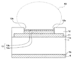
1b…半導体基板の基板裏面、4…裏面電極としてのコレクタ電極、
4b…コレクタ電極のNi膜、10…半導体装置としての半導体チップ、
11…Al電極、13…金属電極、13a…Niメッキ層、
13b…Auメッキ層、100…半導体ウェハ。
Claims (5)
- 半導体基板(1)における素子が形成された面である基板表面(1a)にアルミニウムからなるアルミニウム電極(11)を備え、前記半導体基板における前記基板表面とは反対側の基板裏面(1b)に裏面電極(4)を備えてなる半導体装置において、
前記アルミニウム電極の表面には、メッキ形成されたニッケルメッキ層(13a)を含む積層構造の外部接続用の金属電極(13)が形成されており、
前記裏面電極は物理的気相成長法により形成されたニッケル膜(4b)を含む積層構造の電極であり、前記ニッケル膜の膜応力が前記金属電極における前記ニッケルメッキ層の膜応力の3倍以上であることを特徴とする半導体装置。 - 前記ニッケル膜(4b)の膜応力が2.7×10⁸Pa以上であり、前記ニッケルメッキ層(13a)の膜応力が8.9×10⁷Pa以下であることを特徴とする請求項1に記載の半導体装置。
- 前記半導体基板(1)の厚さが200μm以下であることを特徴とする請求項1または2に記載の半導体装置。
- 前記半導体基板(1)の前記基板表面(1a)の全面積に対する前記アルミニウム電極(11)の占める占有面積の比率が30%以上であることを特徴とする請求項1ないし3のいずれか一つに記載の半導体装置。
- 前記金属電極(13)上にはSnを主成分とするはんだが接続されるものであり、前記ニッケルメッキ層(13a)の膜厚は少なくとも5μm以上に調整されていることを特徴とする請求項1ないし4のいずれか一つに記載の半導体装置。
Priority Applications (1)
| Application Number | Priority Date | Filing Date | Title |
|---|---|---|---|
| JP2003273455A JP3767585B2 (ja) | 2003-07-11 | 2003-07-11 | 半導体装置 |
Applications Claiming Priority (1)
| Application Number | Priority Date | Filing Date | Title |
|---|---|---|---|
| JP2003273455A JP3767585B2 (ja) | 2003-07-11 | 2003-07-11 | 半導体装置 |
Publications (2)
| Publication Number | Publication Date |
|---|---|
| JP2005033130A JP2005033130A (ja) | 2005-02-03 |
| JP3767585B2 true JP3767585B2 (ja) | 2006-04-19 |
Family
ID=34210688
Family Applications (1)
| Application Number | Title | Priority Date | Filing Date |
|---|---|---|---|
| JP2003273455A Expired - Lifetime JP3767585B2 (ja) | 2003-07-11 | 2003-07-11 | 半導体装置 |
Country Status (1)
| Country | Link |
|---|---|
| JP (1) | JP3767585B2 (ja) |
Families Citing this family (14)
| Publication number | Priority date | Publication date | Assignee | Title |
|---|---|---|---|---|
| JP4788390B2 (ja) * | 2005-06-07 | 2011-10-05 | 株式会社デンソー | 半導体装置の製造方法 |
| JP2007194514A (ja) | 2006-01-23 | 2007-08-02 | Mitsubishi Electric Corp | 半導体装置の製造方法 |
| JP4973046B2 (ja) * | 2006-07-20 | 2012-07-11 | 株式会社デンソー | 半導体装置の製造方法 |
| WO2010117987A1 (en) * | 2009-04-08 | 2010-10-14 | Efficient Power Conversion Corporation | Bumped, self-isolated gan transistor chip with electrically isolated back surface |
| JP5672685B2 (ja) * | 2009-09-29 | 2015-02-18 | 富士電機株式会社 | 半導体装置の製造方法 |
| JP5575444B2 (ja) * | 2009-09-29 | 2014-08-20 | 富士電機株式会社 | 半導体装置の製造方法 |
| KR101998340B1 (ko) * | 2012-07-18 | 2019-07-09 | 삼성전자주식회사 | 전력 소자 모듈 및 그 제조 방법 |
| EP2993690A4 (en) * | 2013-11-22 | 2017-01-18 | Fuji Electric Co., Ltd. | Silicon carbide semiconductor device and method for producing silicon carbide semiconductor device |
| JP2015109334A (ja) * | 2013-12-04 | 2015-06-11 | 株式会社デンソー | 半導体装置 |
| JP6300236B2 (ja) * | 2015-02-26 | 2018-03-28 | 株式会社日立製作所 | 半導体装置、半導体装置の製造方法および電力変換装置 |
| DE102015104570B4 (de) | 2015-03-26 | 2019-07-11 | Infineon Technologies Ag | Leistungs-chip und chipanordnung |
| WO2016163319A1 (ja) * | 2015-04-06 | 2016-10-13 | 三菱電機株式会社 | 半導体素子及びその製造方法 |
| JP6698499B2 (ja) | 2016-11-15 | 2020-05-27 | ルネサスエレクトロニクス株式会社 | 半導体装置およびその製造方法 |
| JP2024134749A (ja) * | 2023-03-22 | 2024-10-04 | 三菱電機株式会社 | 半導体装置、電力変換装置および半導体装置の製造方法 |
Family Cites Families (7)
| Publication number | Priority date | Publication date | Assignee | Title |
|---|---|---|---|---|
| JPS58122782A (ja) * | 1982-01-14 | 1983-07-21 | Nippon Telegr & Teleph Corp <Ntt> | ダイオ−ド |
| JPS63305532A (ja) * | 1987-06-05 | 1988-12-13 | Toshiba Corp | バンプの形成方法 |
| JPH0784647B2 (ja) * | 1988-09-15 | 1995-09-13 | 日本電装株式会社 | ニッケル膜およびそれを形成するスパッタリング方法 |
| JPH06216065A (ja) * | 1993-01-20 | 1994-08-05 | Matsushita Electric Ind Co Ltd | 半導体装置の製造方法 |
| JP3601432B2 (ja) * | 2000-10-04 | 2004-12-15 | 株式会社デンソー | 半導体装置 |
| JP2003110064A (ja) * | 2001-07-26 | 2003-04-11 | Denso Corp | 半導体装置 |
| JP2004221416A (ja) * | 2003-01-16 | 2004-08-05 | Toyota Industries Corp | 半導体装置の製造方法及びその半導体装置 |
-
2003
- 2003-07-11 JP JP2003273455A patent/JP3767585B2/ja not_active Expired - Lifetime
Also Published As
| Publication number | Publication date |
|---|---|
| JP2005033130A (ja) | 2005-02-03 |
Similar Documents
| Publication | Publication Date | Title |
|---|---|---|
| JP5413707B2 (ja) | 金属−セラミック複合基板及びその製造方法 | |
| JP6250864B2 (ja) | パワー半導体装置 | |
| JP5141076B2 (ja) | 半導体装置 | |
| US7880285B2 (en) | Semiconductor device comprising a semiconductor chip stack and method for producing the same | |
| JP4049035B2 (ja) | 半導体装置の製造方法 | |
| US7030496B2 (en) | Semiconductor device having aluminum and metal electrodes and method for manufacturing the same | |
| JP2005520339A (ja) | ウエハレベルのコーティングされた銅スタッドバンプ | |
| CN101221915B (zh) | 功率mosfet的晶片级芯片规模封装 | |
| US10026695B2 (en) | Semiconductor device and method for manufacturing the same | |
| JP2005033130A (ja) | 半導体装置 | |
| JP4604641B2 (ja) | 半導体装置 | |
| JP2006261569A (ja) | サブマウントおよびその製造方法 | |
| US20200161234A1 (en) | Semiconductor package structure and method of making the same | |
| JP2023174895A (ja) | 半導体素子および半導体装置 | |
| US7425503B1 (en) | Apparatus and method for enhanced thermal conductivity packages for high powered semiconductor devices | |
| JP2005019922A (ja) | 半導体パッケージ用リードフレーム | |
| US20210104449A1 (en) | Power Semiconductor Package with Highly Reliable Chip Topside | |
| US7678609B2 (en) | Semiconductor package with redistributed pads | |
| JP2007005368A (ja) | 半導体装置の製造方法 | |
| US20220238425A1 (en) | Semiconductor package structure | |
| WO2007034791A1 (ja) | 半田層及びこれを用いた放熱基板並びにその製造方法 | |
| CN111490018A (zh) | 具有金属导热凸块接垫的陶瓷基板元件、组件及制法 | |
| JP2019125758A (ja) | 半導体装置の製造方法 | |
| JP2006261415A (ja) | 半導体装置の製造方法 | |
| JP2016219749A (ja) | 半導体装置および半導体装置の製造方法 |
Legal Events
| Date | Code | Title | Description |
|---|---|---|---|
| A977 | Report on retrieval |
Free format text: JAPANESE INTERMEDIATE CODE: A971007 Effective date: 20051026 |
|
| A131 | Notification of reasons for refusal |
Free format text: JAPANESE INTERMEDIATE CODE: A131 Effective date: 20051129 |
|
| A521 | Request for written amendment filed |
Free format text: JAPANESE INTERMEDIATE CODE: A523 Effective date: 20051205 |
|
| TRDD | Decision of grant or rejection written | ||
| A01 | Written decision to grant a patent or to grant a registration (utility model) |
Free format text: JAPANESE INTERMEDIATE CODE: A01 Effective date: 20060110 |
|
| A61 | First payment of annual fees (during grant procedure) |
Free format text: JAPANESE INTERMEDIATE CODE: A61 Effective date: 20060123 |
|
| R150 | Certificate of patent or registration of utility model |
Free format text: JAPANESE INTERMEDIATE CODE: R150 Ref document number: 3767585 Country of ref document: JP Free format text: JAPANESE INTERMEDIATE CODE: R150 |
|
| FPAY | Renewal fee payment (event date is renewal date of database) |
Free format text: PAYMENT UNTIL: 20090210 Year of fee payment: 3 |
|
| FPAY | Renewal fee payment (event date is renewal date of database) |
Free format text: PAYMENT UNTIL: 20100210 Year of fee payment: 4 |
|
| FPAY | Renewal fee payment (event date is renewal date of database) |
Free format text: PAYMENT UNTIL: 20110210 Year of fee payment: 5 |
|
| FPAY | Renewal fee payment (event date is renewal date of database) |
Free format text: PAYMENT UNTIL: 20120210 Year of fee payment: 6 |
|
| FPAY | Renewal fee payment (event date is renewal date of database) |
Free format text: PAYMENT UNTIL: 20130210 Year of fee payment: 7 |
|
| FPAY | Renewal fee payment (event date is renewal date of database) |
Free format text: PAYMENT UNTIL: 20140210 Year of fee payment: 8 |
|
| R250 | Receipt of annual fees |
Free format text: JAPANESE INTERMEDIATE CODE: R250 |
|
| R250 | Receipt of annual fees |
Free format text: JAPANESE INTERMEDIATE CODE: R250 |
|
| R250 | Receipt of annual fees |
Free format text: JAPANESE INTERMEDIATE CODE: R250 |
|
| R250 | Receipt of annual fees |
Free format text: JAPANESE INTERMEDIATE CODE: R250 |
|
| R250 | Receipt of annual fees |
Free format text: JAPANESE INTERMEDIATE CODE: R250 |
|
| R250 | Receipt of annual fees |
Free format text: JAPANESE INTERMEDIATE CODE: R250 |
|
| R250 | Receipt of annual fees |
Free format text: JAPANESE INTERMEDIATE CODE: R250 |
|
| R250 | Receipt of annual fees |
Free format text: JAPANESE INTERMEDIATE CODE: R250 |
|
| R250 | Receipt of annual fees |
Free format text: JAPANESE INTERMEDIATE CODE: R250 |
|
| R250 | Receipt of annual fees |
Free format text: JAPANESE INTERMEDIATE CODE: R250 |
|
| EXPY | Cancellation because of completion of term |