JP3774538B2 - Personal computer circuit, computer system, and operation method thereof - Google Patents
Personal computer circuit, computer system, and operation method thereof Download PDFInfo
- Publication number
- JP3774538B2 JP3774538B2 JP08421097A JP8421097A JP3774538B2 JP 3774538 B2 JP3774538 B2 JP 3774538B2 JP 08421097 A JP08421097 A JP 08421097A JP 8421097 A JP8421097 A JP 8421097A JP 3774538 B2 JP3774538 B2 JP 3774538B2
- Authority
- JP
- Japan
- Prior art keywords
- dsp
- microprocessor
- memory
- main cpu
- pci
- Prior art date
- Legal status (The legal status is an assumption and is not a legal conclusion. Google has not performed a legal analysis and makes no representation as to the accuracy of the status listed.)
- Expired - Fee Related
Links
Images


Classifications
-
- G—PHYSICS
- G06—COMPUTING OR CALCULATING; COUNTING
- G06F—ELECTRIC DIGITAL DATA PROCESSING
- G06F9/00—Arrangements for program control, e.g. control units
- G06F9/06—Arrangements for program control, e.g. control units using stored programs, i.e. using an internal store of processing equipment to receive or retain programs
- G06F9/46—Multiprogramming arrangements
- G06F9/50—Allocation of resources, e.g. of the central processing unit [CPU]
-
- G—PHYSICS
- G06—COMPUTING OR CALCULATING; COUNTING
- G06F—ELECTRIC DIGITAL DATA PROCESSING
- G06F13/00—Interconnection of, or transfer of information or other signals between, memories, input/output devices or central processing units
- G06F13/14—Handling requests for interconnection or transfer
- G06F13/20—Handling requests for interconnection or transfer for access to input/output bus
- G06F13/28—Handling requests for interconnection or transfer for access to input/output bus using burst mode transfer, e.g. direct memory access DMA, cycle steal
-
- G—PHYSICS
- G06—COMPUTING OR CALCULATING; COUNTING
- G06F—ELECTRIC DIGITAL DATA PROCESSING
- G06F13/00—Interconnection of, or transfer of information or other signals between, memories, input/output devices or central processing units
- G06F13/38—Information transfer, e.g. on bus
- G06F13/40—Bus structure
- G06F13/4004—Coupling between buses
- G06F13/4009—Coupling between buses with data restructuring
- G06F13/4018—Coupling between buses with data restructuring with data-width conversion
-
- G—PHYSICS
- G06—COMPUTING OR CALCULATING; COUNTING
- G06F—ELECTRIC DIGITAL DATA PROCESSING
- G06F13/00—Interconnection of, or transfer of information or other signals between, memories, input/output devices or central processing units
- G06F13/38—Information transfer, e.g. on bus
- G06F13/40—Bus structure
- G06F13/4004—Coupling between buses
- G06F13/4027—Coupling between buses using bus bridges
-
- G—PHYSICS
- G06—COMPUTING OR CALCULATING; COUNTING
- G06F—ELECTRIC DIGITAL DATA PROCESSING
- G06F15/00—Digital computers in general; Data processing equipment in general
- G06F15/76—Architectures of general purpose stored program computers
- G06F15/78—Architectures of general purpose stored program computers comprising a single central processing unit
- G06F15/7839—Architectures of general purpose stored program computers comprising a single central processing unit with memory
- G06F15/7864—Architectures of general purpose stored program computers comprising a single central processing unit with memory on more than one IC chip
-
- G—PHYSICS
- G06—COMPUTING OR CALCULATING; COUNTING
- G06F—ELECTRIC DIGITAL DATA PROCESSING
- G06F9/00—Arrangements for program control, e.g. control units
- G06F9/06—Arrangements for program control, e.g. control units using stored programs, i.e. using an internal store of processing equipment to receive or retain programs
- G06F9/30—Arrangements for executing machine instructions, e.g. instruction decode
- G06F9/38—Concurrent instruction execution, e.g. pipeline or look ahead
- G06F9/3877—Concurrent instruction execution, e.g. pipeline or look ahead using a secondary processor, e.g. coprocessor
- G06F9/3879—Concurrent instruction execution, e.g. pipeline or look ahead using a secondary processor, e.g. coprocessor for non-native instruction execution, e.g. executing a command; for Java instruction set
-
- G—PHYSICS
- G06—COMPUTING OR CALCULATING; COUNTING
- G06F—ELECTRIC DIGITAL DATA PROCESSING
- G06F9/00—Arrangements for program control, e.g. control units
- G06F9/06—Arrangements for program control, e.g. control units using stored programs, i.e. using an internal store of processing equipment to receive or retain programs
- G06F9/46—Multiprogramming arrangements
- G06F9/54—Interprogram communication
- G06F9/544—Buffers; Shared memory; Pipes
-
- G—PHYSICS
- G06—COMPUTING OR CALCULATING; COUNTING
- G06F—ELECTRIC DIGITAL DATA PROCESSING
- G06F2209/00—Indexing scheme relating to G06F9/00
- G06F2209/50—Indexing scheme relating to G06F9/50
- G06F2209/509—Offload
Landscapes
- Engineering & Computer Science (AREA)
- Theoretical Computer Science (AREA)
- General Engineering & Computer Science (AREA)
- Software Systems (AREA)
- Physics & Mathematics (AREA)
- General Physics & Mathematics (AREA)
- Computer Hardware Design (AREA)
- Advance Control (AREA)
- Microcomputers (AREA)
- Stored Programmes (AREA)
Abstract
Description
【0001】
【発明の属する技術分野】
本発明は、一般に改善されたパーソナルコンピュータ(以下、PCと称する)回路、コンピュータシステム、及びこれらの動作方法に関する。
【0002】
【発明が解決しようとする課題】
初期のコンピュータは、大きな空間を要し、室全体を占めた。時来、ミニコンピュータ及びデスクトップコンピュータが市場に出回ってきた。
【0003】
普及しているデスクトップコンピュータには、「Apple(商標)」(Motorola(商標)680x0 マイクロプロセッサベース)及び「IBM(商標)−互換機」(Intel(商標)又はその他のx86マイクロプロセッサベース)等多種のものがあり、これらはPCとして知られ、オフィス及び家庭での使用に非常に普及してきている。また、いくつかのスーパスカラ及びSuperSPARC(商標)のような他の非常に高性能マイクロプロセッサに基づくワークステーションと呼ばれるハイエンド(high end)デスクトップコンピュータも導入されている。
【0004】
更に発展して、ノートブック寸法又はパームトップコンピュータが、携帯ユーザ応用のためにオプショナルに電池式を採っている。このようなノートブック及び小形コンピュータは、ミニチュア化、絶えずより高速、より高性能、より融通性及び充電間電池の長寿命化と云う相容れない目標を迫られる技術に挑戦している。また、ドッキングステーションと呼ばれるデスクトップ密閉容器はドッキングステーション内へはめ込まれる携帯用コンピュータを有し、かつこのような携帯用コンピュータ/ドッキングステーションシステムの改善が望まれる。しかしながら、これら全てのシステムは、一般に、中央処理装置(以下、CPUと称する)の選択がシステムの処理能力を決定しかつアドインカード(add−in−card)、すなわち、組込みカードがCPUに付加されて、モデム、マルチメディアのような特定応用又は機能を付加すると云う意味でCPU中心的である。回路、集積回路デバイス、あらゆる型式のコンピュータシステムにおける改善、かつ、なかでも、いま上に挙げた挑戦に取り組む方法が、本明細書に説明するように望まれる。
【0005】
【課題を解決するための手段】
全体的に、かつ本発明の1つの形では、PCシステムは、主CPUマイクロプロセッサ、ファイルベースオペレーティングシステム、及びディジタル信号処理装置(以下、DSPと称する)マイクロプロセッサを含み、これらは主CPUが他に係わって占有されている時間間隔中DSPが主CPU動作を実行することができるように配置され、それによってこのPCシステムの帯域幅を広げる。このPCシステムは、多数のCPU及び(又は)多数のDSPを含むこともできる。
【0006】
本発明の他の形では、DSPマイクロプロセッサ、ビデオ/オーディオ制御論理回路、及び圧縮/伸張電子回路を含む組合わせビデオ/作像システムが、共に、DSPマイクロプロセッサ、主CPUマイクロプロセッサ、これら両マイクロプロセッサに結合されたメモリ管理回路、及びメモリ回路をメモリ管理路に結合するメモリ回路とローカルバスに結合され、それであるから、メモリ回路がDSP、主CPU、ビデオ/オーディオ制御論理回路、及び圧縮/伸張電子回路に対する統一メモリアーキテクチャとして働き、かつDSPがビデオ/オーディオ制御論理回路及び圧縮/伸張電子回路の両方に関する処理機能を遂行する。加えて、ビデオ/作像機能の部分を仮想化するソフトウェアがこのシステムに付加されることがある。
【0007】
本発明は、PCを総合的にソフト高度化するシステムを提供する。
【0008】
本発明は、アドインカードを通してアドイン特徴、すなわち、組込み特徴をまとめて取り扱うことによって性能を向上するシステムを提供する。
【0009】
本発明は、マザーボード実現のためにコア論理内の特徴を集積化する方法論を提供する。
【0010】
本発明は、CPUチップ上にシステムの全機能集積化する。
【0011】
本発明は、主CPU、DSP、及び実質的に物理層のみに減少したアプリケーションハードウェアの少なくとも1つの片を有し、それであるからそのDSPがこの物理層によって媒介される信号に関連したアプリケーションの残りを仮想化しかつ遂行するシステムを提供する。このシステムは、多数のアプリケーション及び層を採用することがある。DSPは、例えば、ローカルエリアネットワーク(以下、LANと称する)、ビデオコントローラ、画像圧縮/伸張電子回路、ファックス、及びモデムを仮想化する。
【0012】
本発明は、DSPコア、マスタ/スレーブバスインタフェース、このインタフェースに結合された先入れ先出し(以下、FIFOと称する)機能を含むメモリ回路、及びDSPコアに結合されたRAM機能を有する集積回路を提供する。
【0013】
本発明は、DSPコア、マスタ/スレーブバスインタフェース、及びこのインタフェースに結合されたFIFO機能を含むメモリ回路、及びこのメモリをDSPコアに結合する単一命令/多重データ制御回路を含む集積回路を提供する。
【0014】
本発明は、DSPコア、マスタ/スレーブバスインタフェースと翻訳回路を含むインタフェース回路、マスタスレーブバスインタフェースに結合されたFIFO機能と翻訳回路に結合されたRAM機能を含むメモリ回路を有し、前記DSPコアが前記メモリ回路とインタフェースに結合される集積回路を提供する。
【0015】
本発明は、第1バスインタフェース回路、ディスプレイインタフェースを有するディスプレイコントローラ回路、及び第2バスインタフェース回路を有し、前記ディスプレイコントローラ回路が前記第2バスインタフェース回路に結合されたバスマスタリング回路を含むビデオコントローラ集積回路を提供する。
【0016】
本発明は、次のようなソフトウェアシステムを提供する。すなわち、オペレーティングシステム、少なくとも1つのマルチメディアドライバ、x86オブジェクトコードアプリケーション、ハードウェアアプリケーションを仮想化する非x86DSPコードアプリケーション、及びDSPカーネルソフトウェアを有するソフトウェアシステムであって、このカーネルソフトウェアが、オペレーティングシステム及び(又は)マルチメディア実時間事象と関連して、実時間割り込み、及び(又は)直接メモリアクセス(以下、DMAと称する)仮想化及び(又は)DSPコア内でのマルチスレッドマルチタスキングオペレーションを遂行するためにDSPコア上で動作可能であり、及び(又は)DSPコアに、そうでなければx86によって遂行されるメモリトランザクション機能及び(又は)入出力(以下、I/Oと称する)トランザクション機能を遂行させる。
【0017】
本発明は、処理素子、前記処理素子に接続された相互接続回路、前記処理素子(又は前記相互接続回路)に接続されたメモリ電子回路、前記相互接続回路に接続された多重化バス、及び予め選択されたアプリケーション機能を遂行するために前記多重化バスに接続された仮想化回路を有す計算システムを提供する。
【0018】
本発明は、第1多重化バスインタフェース回路、第2多重化バスインタフェース回路、及び前記第1多重化バスインタフェース回路と第2多重化バスインタフェース回路に接続された少なくとも1つの信号処理素子を有する予め選択されたアプリケーション機能を遂行する仮想化回路を提供する。
【0019】
他の改善されたPC装置、システム、及びこれらの動作方法もまた特許請求の範囲で請求される。
【0020】
本発明は、添付図面と関連して次の詳細な説明を参照することによって理解される。
【0021】
これらの添付図面において、もし他に指示がなければ、同一機能を有する部品は同一符号で示してある。
【0022】
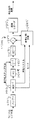
【発明の実施の形態】
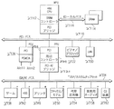
図27を初めに参照すると、本発明の改善されたPC100のブロック図が示されている。図27で、マイクロプロセッサユニット(MicroProcessor Unit、以下、MPUと称する)ブロック2702は、486(又はP5)CPU、又はx86CPUの他のいずれかの型式、ダイナミックRAM(以下、DRAMと称する)コントローラ回路、及び周辺デバイス相互接続(以下、PCIと称する)ブリッジ回路を含む。PC100は、マルチメディアアプリケーション能力を有する。
【0023】
ローカルCPUバス2706は、MPUブロック2702をDRAM2714に接続する。このDRAMは、好適には、少なくとも4Mの容量を有する。もっとも、多かれ少なかれメモリがこのように採用されるのは明白である。ローカルバス2706は、種々のCPUが同じバス上で使用されるようにCPUを独立させて維持するように設計される。
【0024】
PCIバス2710は、CPUブロック2702内のPCIブリッジを経由してブロック2702内のCPUに接続される。このようにして、PCI2710バスは、広い帯域幅バスを提供し、かつまた、そうでなければローカルバス2706を不利にロードするおそれのある多種の周辺デバイスに対してコネクタを提供する。
【0025】
周辺処理装置(以下、PPUと称する)2718は、PCIバス2710をISA/ATバス2734に接続するシステムブリッジとして働く。また、PCMCIAカード又はPCMCIAカードバス用PCMCIAブリッジ2726がPCIバスに接続する。PCIバスに接続されたネットワークブリッジ2730は、LANブリッジと同じように複雑でないものでよく、又は広域ネットワーク(以下、WANと称する)ブリッジ、無線周波数(以下、RFと称する)ブリッジ、非同時伝送モード(以下、ATMと称する)ブリッジ又は総合サービスディジタル網(以下、ISDNと称する)ブリッジであってよい。ブリッジのこれらの型式の各々は、PCIバス上に直接かなり多量のトラフィックを発生し、及びローカルバス2706上に間接にかなりのトラフィックを発生する。PC100は、ユーザ入力用にこれに接続されたキーボード及びマウス(図27には示されていない)、及びCPU出力のユーザ観察用ディスプレイ又はCRT(図27に示されていない)を有する。
【0026】
図27において、バス2706、2710、及び2734、は、相互接続されていない。ISA/ATバス2734に接続されて、例えば、ゲーム2739、ハードディスク装置2742、プリンタ2746、ファックスデータモデム2750、電話代理応答機(DTADとも称する)2754、業務用オーディオブロック2758、及びマルチメディアPC用CD(コンパクトディスク)装置2762のような、しかしこれらに限定されないオプショナルアクセサリ周辺デバイスの集合が表示されている。これらのISAブロックの各々は、パートタイム機能を遂行するアクセサリ周辺デバイスであり、かつ多くのもの(星印を付されたもの)はDSPを含む。
【0027】
一般に、図27でPCIバス2710に接続された他のブロックは、ISA/ATバス2734に接続された全ての周辺デバイスとほぼ同じ位のコストがかかる。例えば、業務用オーディオシステム2758の総合システムコストは、10ドル未満、すなわち総合PCシステムコストの約0.5%未満のはずである。
【0028】
コスト低減の構図(roadmap)、将来の高度化へと、及び現存する(「遺産」)ソフトウェア目標との互換性は、いずれの改善されたPCシステムにとっても重要な目標である。本発明のシステム実施例は、システムレベルでの改善がこれらの目標を達成し得ることを確認しかつ証明する。特に、システム実施例は、PCマザーボードに含まれるそのいずれもが、好適には、低コスト、ソフトウェア無用、及び本質的に無視可能なマザーボードエリアしか占めないことを確認する。
【0029】
DOS及びWindows(商標)3.11との後方互換性(backward compatibility)が、本発明の「仮想」ハードウェアによって提供されると云える。仮想ハードウェアは、図27に示された全ての機能が固定されかつ専用され、及びたとえこれらの機能が分散されても更新可能でないことを意味する。ソフトウェアは、それらを仮想化するのを助援することができる。もし1チップが図27に示された機能の全てを実現するならば、このチップは非常にプログラマブルなものであろう。したがって、本発明の種々の実施例は、図27に示した全ての冗長なかつ相容れないハードウェアを組み合わせて図27に示された機能の全てを「仮想化」するのに充分にプログラマブルであるいくつかのチップを作成し、かつ、最終的に、これらの機能を遂行する単一チップを提供する。
【0030】
Windowsは、最近及び将来のPC用オペレーティングシステム(以下、OSと称する)であって、かつライブラリにダイナミックにリンクし、それであるからソフトウェアは実行時間前にコンパイルされかつリンクされなくてよく、例えば、ダイナミックリンクローディング(以下、DLLと称する)はラン時間までリンクされず、かつ仮想ソフトウェアを提供する。これが、ソフトウェア寸法を縮小する。
【0031】
一般に、従来のCPUシステムは、種々のアプリケーションを実現するために固定CPUハードウェアを使用するが、しかしそのCPUはATバス又は図27に示された全てのI/Oポートに係わることでがきない。本明細書に後に説明される本発明の一実施例では、ハードウェアがこれを正にできるようにする。
【0032】
マルチメディアアプリケーション用に、システムブリッジ2718内のDMA2719及び割り込みコントローラ2720が、固定ハードウェア及び固定機能を有する。本発明の一実施例では、DMA及び割り込み制御は仮想化される。マルチメディアをサービスするに当たって2つの鍵になる挑戦が、マルチメディアデータ用広帯域幅に及び実時間割り込みをサービスする能力に必要である。これらの挑戦は、障害、及び実時間事象をサービスする能力に制約又は限界を持ち込む割り込み可能性を生じることがある。これの全てを、本発明の実施例では、ハードウェアを仮想化して、例えば、ハードウェアを多数の個性を帯びるようにプログラマブルにすることによって克服する。ハードウェアが割り込みハンドラ(handler)の個性を帯びるとき、それはCPUの部分又はそうでなければ実時間能力のあるCPU及びOSの拡張であって、コプロセッサ又は付属装置ではない。
【0033】
仮想ハードウェアは、同時にCPU内とOS内とに係わる移動性を有する。これを物理的に達成する方法は知られていないので、本発明の教示に従って仮想化が実現される。プログラマブルであるDSP解決及びコアは、仮想ハードウェアの基礎として働き、これは、本明細書に説明されるようにカスタム化されかつ改善される。
【0034】
DSPコアは、本発明の実施例に必要な種々の仮想化をランするために高度に有利な基礎である。しかしながら、DSPはメモリ周辺デバイス及びローカルDSPバスを利用し、これが更に加わる挑戦を導入する。本発明の教示を使用すると、正反対に異なるDSPが、Pentium(R)のような、x86CPUのように「見える」ように作られ、又はこの逆にも作られる。
【0035】
ソフトウェアリンクが、DSPとその周辺デバイスをx86CPUに緊密に結合するために使用され、かつ、これを行うのに、例えば、Windows95のような、しかしこれに限定されない、普及したOSを使用する。このソフトウェアリンクは、DSPとその周辺デバイスが同じチップ上にある場合よりもこれら2つを緊密に結合する。それゆえ、ことごとくがソフトウェアに作られ、ハードウェアとソフトウェアとの間の線がはっきりしておらず、或る著しい利点を達成する。結局、電話線によって又は制御情報転送によって遠隔的に高度化可能なソフトウェアを有する単一チップが得られる。
【0036】
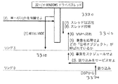
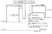
図19aは、Windows3.11内で支配的な層構造アーキテクチャを示す。アプリケーションブロック1902は、音声アプリケーションのような、マルチメディアアプリケーションである。ブロック1902の下の普通ブロックは、独立系ソフトウェアベンダー(以下、ISV)にトランスペアレントである。Windowsアプリケーションは、クライアント/サーバモデルを使用し、この場合アプリケーションはクライアントであり、かつサーバはそのリクエストを取り扱うものは何でもそうである。そのリクエスリトの発する方(issue)が、多くの場合、正しいサーバが見つけている。ブロック1906は、ブロック1902の下の第1層MMSYSTEM(マルチメディアシステム)であり、マルチメディアハードウェアと通信し、かつ音声 .WAVファイルを再生する。Windows.WAV ドライバブロック1910は、このシステム内の第2層又は第1ドライバ層であり、アプリケーション1902からのリクエストを取り扱い、かつ圧縮を伴わず .WAVフォーマットで信号を再生する。CPU環境内の最下層は、DSPドライバ1914であり、これはハードウェア適合層(以下、HALと称する)内のハードウェアを仮想化する仮想デバイスドライバである。オーディオ圧縮マネージャ(以下、AVMと称する)ドライバ1918は、システム内に圧縮/伸張機能性を提供し、かつブロック1914と通信する。これは、CPU2702側からの画像マッピングを完全にする。
【0037】
これは、クライアント/サーバアーキテクチャへプラグインする方法をWindowsアーキテクチャ内に提供する。それゆえ、Windowsを通してDSPサーバ又はオーディオ圧縮サーバをプラグインすることができ、それらの機構はどれも同じである。図19aは、所望のどれかのアーキテクチャをWindowsにプラグインする方法を示す。また、これは、後方互換性に対する鍵であると共に、将来への優れた(bland)新たな非浸入性の(nonintrusive)構図を確立する。
【0038】
次に、図19bで、仮想ハードウェア環境1922が、既に利用可能な最大第3者設置ソフトウェアベース(例えば、モデム、オーディオ機器等)に適合する特別DSPカーネルソフトウェアを備えたTI TMS320C5x DSPで以て、しかしこれに限定されることなく、実現されている。ことごとくがプリエンプティブ割り込み(preemptive)ベースでランし、及び優先権が実時間に計算されかつダイナミックに実行される。しかしながら、OSが実時間に優先権を計算することができるように或る何かがOSを供給しなければならない。その或る何かが実時間カーネルソフトウェア1922である。これはWindows OSを補完し、かつこれと相容れないようなことはなく、これを拡張するように働く。これによって、マルチスレッドかつマルチタスキングシステムが提供される。
【0039】
次に、オーディオコンバータブロック1926がDSP側上でオーディオ圧縮/伸張を遂行するのに対して、ACMドライバブロック1918がCPU側で同じ機能を果たすこともできる。しかしながら、もしそのCPUが占有されており、この機構を遂行する時間を持たないならば、DSPがそれを取り扱うことがある。もしCPUもDSPも自由ならば、CPUとDSPの間の線をはっきりさせないソフトウェアの能力のために、これらのいずれか又は両方がこの機能を行うことができる。それゆえ、全て、OSを通しての有利な結果として、CPUはDSPを体現でき、かつDSPはCPUを体現できる。従来、CPUはデータ移動を遂行するが、これはCPUが32又は64ビットチャンクで移動を遂行できるからである。しかしながら、本発明では、DSPに対するアプリケーション呼び出し内のアルゴリズム性の強い(algorithumic intensive)ブロックがそれを行う。このようにして、アプリケーションが加速されると云える。
【0040】
DSPコーデックドライバ1930は、ステレオコーデック1934に結合する。好適には、このシステム実施例の場合、コーデック更新を考慮に入れるために、DSPに対して1チップを外部ステレオコーデック1934と共に適当に使用する。
【0041】
図1は、本発明の改善されたPCシステム100のブロック図を示す。図1で、PCシステム100はCPU102を含み、このCPUはキャッシュ104及びホストブリッジ108に接続される。ホストブリッジ108は、主メモリバス106(ときには、CPUバス又はローカルバスと称する)に接続され、これによって主メモリ112に、かつまたPCIバス116に接続される。PCシステム100は、ユーザ入力用にこれに接続された典型的にキーポード及び(又は)マウス(図1には示されていない)、及びCPU出力のユーザ観察用ディスプレイ又はCRT(図1には示されていない)を有する。仮想DSP回路200は、PCIバス116に接続される。システム100用に低速から高速直列キャプチャポートを実現するP1394/USB(上側波帯)ブロック120は、PCIバス116に接続される。I/Oブロック124は、図1に示されており、PCIバス116に接続される。このI/Oブロック124は、ATM/LAN、ISDN又はRFリンクであってよい。DSPブロック200は、これらの種々の全てのI/Oシステムにオプショナルに接続する。
【0042】
DSP200は、ブロック124の上掲の機能又はアプリケーションを遂行するために必要なハードウェアを「仮想化」するDSP200の能力があるので、I/Oブロック124を包含する又は置換することができる。
【0043】
図1で、DSPブロック200に適当なモデムソフトウェアを備えることによって過去のモデムが仮想化されている。仮想化されることがある他の類似のアプリケーションは、スピーカホーン、スピーチ、DSVD(digital simultaneous voice and data modem)、T.120トランスポート層、VDSVD(video digital simultaneous voice and data)である。図1の「長円形ブロック」は、これらアプリケーションの或るものを示す。
【0044】
他の仮想化可能アプリケーションには、ビデオ圧縮/伸張用ベクトル量子化(以下、VQと称する)、ビデオ圧縮/伸張用MPEG、ISDNに基づく室内会議H.320、ATN及びLANに基づくH.321、H.322、及び電話線によるテレビ会議がある。
【0045】
更に他の仮想化可能アプリケーションには、3次元グラフィック表示アプリケーション、及び移送指向性オーディオ用3次元音声がある。
【0046】
このようなアプリケーションの多くは、業務用オーディオ、ゲーム、ハードディスク装置、プリンタ、ファックスデータモデム、電話代理応答機(DTAD)、マルチメディア用CD装置、及びデータ/ファイル圧縮があり、後者はシステムトラフィック及びCPU負担を軽減するためにDSPによって実行され、またフォーマット変換、及びディジタルフィルタとディジタル変換がある。
【0047】
図1に、P1394/USBブロック120を含めてあるが、これは国内市場はPCを表向き家庭器具として供給しているが、常時運転しているとは限らないと認めるためである。例えば、PCは、簡単にオン、オフスイッチされ、ユーザはこれにインタフェースしない。1つはUSB用、1つはP1394用に2つのケーブルがこのPCに接続され、かつRFインタフェースが同様に接続されることがある。ユーザは電話代理応答機を欲するとき、低コスト電話機を持つ、すなわち、その電話機はこれからPCのUSBジャックへ延びるUSBケーブルを持つ、また同様に通常の壁取り付け電話ジャックへの線を持つ。もしPCがその家の他の部屋内にあるならば、RFが使用されるか、又はその家がP1394に対して配線される。
【0048】
セルラ電話からコストを借り出すために、ハードウェアをセルラ電話の設計から除去し、PCへ移す。それゆえ、セルラ電話は、もはや孤立したシステムでない。
【0049】
それゆえ、各家庭アプリケーション毎に、現在知られているようにハードウェアをそのアプリケーションから除去して、このハードウェアを仮想化するPCへ移す。
【0050】
I/Oブロック124のRFハードウェアも同様にその物理層だけになるように仮想化される。それゆえ、PCシステムは、真に多機能化かつマルチタスキングである。
【0051】
図2は、本発明の改善されたPCシステム100の仮想DSPブロック200の更に詳細なブロック図を示す。図2で、ブロック200は、PCIバス116及びISAバス128に接続されている。他の実施例では、ブロック200がなおまたローカルバス106にも接続される。
【0052】
図2で、PCIバス116はハードウェアインタフェース電子回路210に接続され、このインタフェースが第1層に接続され、この層が次にインタフェース電子回路214に接続され、この回路が次に2つのテキサスインスツルメンツTMS320C5x DSPコア218及び222に結合される。電子回路210は、スピーチトランスコーディング用PCIスレーブインタフェース(Truespeech Slave)、Windowsベースモデムデータポンプ用PCIスレーブインタフェース(WinModem Slave)、DMA散乱−収集機能性(scatter−gather)用PCIスーパーバス・マスタインタフェース、I/Oポートに似たサウンドブラスタ(R,Creative Labs)、及びDMAインタフェースを含む。電子回路210及びPCIバス116によって、PCI/ISAブリッジがまたマルチメディア用に確立される。
【0053】
ブロック200の心臓は、1つ以上のDSPコア218、222である。電子回路214はFIFO RAMである、すなわち、電子回路214はハードウェアFIFOでなくてFIFO機能を遂行する主メモリ112、すなわち、RAMの片である。DSPコア218、222にとってRAM112は正規RAMのように見えるのに対して、このインタフェースのPCIバス側にとってRAM112はFIFOのように見える。電子回路214内で沢山の翻訳が行われる。データ及びオペランドは、CPU102とブロック200との間に流れる。CPU102は、バイト又はビット単位で動作しない。たとえCPU102が32又は64ビット単位で動作しても、それはキャッシュ線に基づくキャッシュ104及び主メモリ112を経由するバーストを通して動作する。このデータ流の非互換性が、翻訳に当たって多くのサイクルを消費する。
【0054】
インタフェースハードウェア214は、32又は64ビット幅データ路を取り、そのどれかの部分を抽出してバイトにし、次いで16ビット語をDSPコアに供給するように設計される。それゆえ、単一命令多重データ(以下、SIMDと称する)アーキテクチャに対する複雑命令セットコンピュータ(以下、CISCと称する)又は縮小命令セットコンピュータ(以下、RISCと称する)がインタフェース挑戦を解決するめに実現される。
【0055】
それゆえ、有利上、インタフェース電子回路214は、次の機能を行う。すなわち、1)FIFO互換性バーストとして64又は128ビット幅バーストを流し込む。2)それらを予め選択されたDSPフォーマットに翻訳する。3)DSPコアに対するRAMとして作用する。
【0056】
異なるクロックが異なるチップ上でランするので、DSPコア動作をPCI動作から減結合することによってクロッキング挑戦をブロック210内で解決する。CPU側からは、このシステムは、充分にPCI動作と同期させられる。DSP側からは、このシステムはPCI動作と非同期である。このようにして多数待機状態を回避し、DSP動作速度を上げても、CPUにインタフェースするとき苛酷な停止(grindinghalt)に立ち至ることはない。
【0057】
DMAトランザクションは、好適には、流れ−I/Oに基づく。CPUは仮想空間内で動作するが、DMAは物理空間で働く。翻訳は、CPU102内の古い又は新しいハードウェアに頼ることなく、好適には、Windows95を使用するソフトウェア制御の下にDSPによって遂行される。DSPは、主DMAのエンジンになる。他の実施例では、CPU102内のDMAエンジンをDSP218から減結合することができ、かつDSPコア218及びDSPコア222がDMAエンジンと関連させられる。DSPは、CPU102又はWindowsが望む方法でDMAを組み立てかつ実行する。例えば、100Mbyte/sのDMA処理能力が、現行技術のDMAコアを用いて容易に達成可能である。
【0058】
ブロック210自体は、PCIエージェントであり、かつ動作中以外は、ハードウェア内の単一マスタ、マルチスレーブRCIエージェントであると云う意味においてコストを低減している。ブロック210のバス支配能力によって、全てのスレーブが動作中従動させられるが、しかしアプリケーションによってPCIバスを支配するように呼び出されるとそれを行う能力を有する。ソフトウェアは、適当な構成データによってスレーブをマスタであるように呼び出す。この多重体現インターフェースは、CPUが他に係わって占有されていないならばCPUがポーリングを行う場合に、働く。もしバスマスタリングが要求されるが、しかしCPUが他に係わって占有されているならば、同じことを実現するためにブロック210内のマスタを通してDSPをバスマスタにならせる。それゆえ、同じアプリケーションのために、DSPは、CPU102自体の代わりにホストの資格で働く。
【0059】
Windowsのソフトウェアアーキテクチャは、Windows下でファイルトランザクションのように見えることごとくを要求する。ファイルトランザクションは、メモリトランザクションであり、かつCPU又はDSPのどれがそれらを遂行しようとかまわない。CPUは一時に1つのことを遂行することしかできず、それでDSPがシステム休止時間に作業を行い、休止時間を満たすので、ハードウェアは必要ない。チェリーピック(cherry pick)するかつ休止時間に作業を行うこの能力は、CPUでは遂行することができないこの調査研究の重要な利点である。ビデオチップ、DSP、CPU、…等、これら全てのチップは、ことごとくのトランザクションがメモリトランザクション又はファイルトランザクション(又はこの目的では余り重要でないI/Oトランザクション)でなければならないと云う同じ拘束によって統制される。全ては、OSの下で同等に扱われる。
【0060】
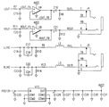
図3は、図1の改善されたコンピュータシステムの部分の一好適実施例の更に詳細な電気回路図(部分的に概略図、部分的にブロック図)である。図3は、図2のハードウェアインタフェース電子回路210及びインタフェース電子回路214を概略的に示す。特に、PCIマスタ/スレーブインタフェース回路304がPCIバス116に接続されていることが判る。PCIマスタ/スレーブインタフェース回路304は、マスタ動作及びスレーブ動作用電子回路を含み、かつハードウェア層305に接続され、この層はPCI構成制御及び状態レジスタ電子回路306、PCI I/O空間レジスタ電子回路308、2重ポート読み出し書き込みFIFO電子回路310、及びDSP I/O空間レジスタ電子回路312を含む。ハードウェア層305は、次にインタフェース/コーデックDMA制御回路316に接続され、後者は次にDSP(図3に示されていない)に接続される。
【0061】
図4aは、図1の改善されたコンピュータシステムの部分の好適実施例の更に詳細な電気回路図(部分的に概略図、部分的にブロック図)である。図4aで、PCIバス116は、マスタ/スレーブインタフェース424へのゲートウェイを経由してマザーボード上又はアドインカード上の単一チップ420に接続される。図4aは、また、PCIバス116に接続される第2チップ460を示す。2つのチップ420、460は、本発明の教示による種々の機能性を区分する2つの異なる方法を示す。
【0062】
チップ420は、オンチップ加速バス343を有しかつ好適にはデスクトップPCである。汎用バスGPI401及びGPI402が、チップ420又は460のどちらか用に備わる(図4aには示されていない)。チップ420内で、IDSP論理ブロック428が図2のブロック200の全ての論理を少なくとも含む。同様に、チップ420のIDSP論理ブロック428が図2のブロック200の全ての論理を少なくとも含む。チップ460は、2つのズームビデオ(以下、ZVと称する)バスを含み、かつ好適には携帯用PC内に使用される。グラフィック/ビデオコントローラ432は、2次元、3次元グラフィック能力ばかりでなく、ビデオ捕獲/圧縮/伸張能力を有する。コントローラ432は、バスマスタであることを要するが、しかし慣例的には常にスレーブである。提案された新しい統一メモリアーキテクチャ(UMAと称する)は、バスマスタを有利にする。
【0063】
典型的又は従来のメモリサイクルは長過ぎるので、メモリも変化しなければならない。メモリは機能性の点では商品であり得ない。それでメモリは追加機能を要し、かつこれを新ブロックにインタフェースさせなければならない。本発明は、この追加機能性を有するメモリの利点を活かす。
【0064】
図4bで、PCIバス116が図4aのDSP/ビデオチップ420に接続されて、PCシステムを形成する。チップ420はメモリコントローラ484に接続され、このコントローラはCPU102との他の結合を有する。メモリコントローラ484及びCPU102は、更に、データバッファ488に結合され、これを制御し、かつこのバッファはローカルバス106上のUMAメモリにアクセスする。データバッファ488を使用することによって、CPUは、また、メモリアクセスを制御するのではなくメモリアクセスをリクエストしなければならない。有利には、ビデオ/グラフィックブロック432の機能が、PCシステム内に合体されている。チップ420は、おそらくパッドバウンド(すなわち、多くのピンを有しかつ要求される全てのパッドに適合するのに必要なシリコンの全てを回路が占めない)であるので、ビデオ/グラフィック機能は有利な空間内に存在する。ここで初めに挙げた種々のアプリケーションの全ては、IDSP加速バスに持ち込まれる。
【0065】
UMAブロック492は、ローエンド(low−end)市場用拡張データ出力DRAM(Extended Data Output DRAM、以下、EDOと称する)を含む。EDOは、不変ピンカウントを有し、486レべルCPUを支持し、かつそのデータ出力は予充電を回避するためにより長く活性に維持される。他の適当なUMAは、キャッシュ線を満たすバースト能力を備える高速EDOである。高レベルUMAは、マルチバンクバーストEDOである。熟練作業員は、特定アプリケーションシステムに望まれる性能及び市場価格点考慮に従ってメモリ型式を選択する。
【0066】
UMAブロック492から、一実施例は、バス106上に最高11Gbyte/sの帯域幅の非圧縮出力を有する。これは、広帯域バス又は500MHz以上で動作するRAMバスのような高速バスのどちらかによって達成されると云える。図4bで、コントローラ432は、UMA492をアクセスしかつ非圧縮ビデオをディスプレイ436(図4bには示されていない)へ送る。広帯域メモリ及びPCIバス116を通してのメモリへのアクセスは、広帯域及び短待ち時間(例えば、2ms)を維持する。
【0067】
図4aの加速バス434は、コントローラ432の加速を考慮するために外部アクセス又は内部アクセスできるようにDSP428に接続される。同様にして、図4bも外部又は内部アクセスをできるように加速バスを含む。
【0068】
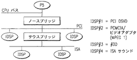
図5は、ホスト依存性である非対称多重処理に対する本発明の改善されたコンピュータシステムの一実施例のブロック図を示す。図5で、P5プロセッサはCPUである。図5で、PC内のどのCPU/IDSPインテリジェンスも、これらをアプリケーションを支持するのに必要な量だけ本発明の仮想技術を介して一括集中することができ、そのアプリケーションが停止した後これを解散することができる。ユーザには、いかなるときにも所与のアプリケーションに要求される計算リソースの所与の量さえあればよい。
【0069】
どれか特定のアプリケーションの必要を満足する多数のIDSPが図5に示されている。これらのチップは、ISAバス及びPCIバスに適当にインタフェースするために異なって設計されている。いくつかの例が図5に示されている。IDSPブロックは、これらのバスに取り付けられて示されているが、これらをノース(north)ブリッジ又はサウス(south)ブリッジのどちらかに取り付けてもよく、及びそのブロックの機能内に集積化してもよい。
【0070】
図6aは、本発明の改善されたコンピュータシステムに対してスーパスカラ拡張を使用するCPUモデルの実施例の概略ブロック図を示す。図6bで、新チップが3つのパイプラインを有し、これらのパイプラインは2つの従来スーパスカラパイプライン及び第3のDSPオペレーションパイプラインである。すなわち、スーパスカラCISC/RISC及びDSP CPUアーキテクチャが単一チップ上にディスパッチされた3つのオペレーションを有する。CISC内にマイクロコード記憶がある。DSPコアはDSPハードウェアマイクロ記憶であり、これはDSPオペレーションをディスパッチする。DSPコアは、ユーザがWindowsアイコンをクリックオンし、次いで、DSPコードが実行のためにハードディスクから主メモリ、ローカルメモリへキャッシュされるまで、「空」でいられる。このようにして、x86CPUは、非標準オペレーション及びディスパッチDSPオペレーションを行わなくて済む。このような組合わせアーキテクチャは、Windows95と互換性である。
【0071】
図6bは、1つのこのようなメモリキャッシュ階層構造を示す。ディスク記憶装置2742は、図6bに定義されたスペクトルの1極にある。次は、主メモリ112である。外部単一アクセスメモリは、ISAバス、PCIバス上のどれか他のメモリ、又はチップ200内の又は図6bの第3レベルのPCシステム内の他の何処かにあるメモリ214である。第2レベルに、構成可能(configurable)DSPコア・アドオンメモリ内のように、単一アクセスオンチップメモリが備わっている。第1レベルに、テキサスインツルメンツTMS320CxコアのB0、B1、B2メモリを有する2重アクセスオンチップDSPコアメモリが、例示として、しかしこれに限られる訳でなく、備わっている。
【0072】
これは、キャッシュ動作するブロック210及びキャッシュ動作するCPU、OSを備えるソフトウェアキャッシュである。それゆえ、DSPはソフトウェア内でキャッシュ動作サイクルを組み立て、かつ制御が階層構造を上へ過ぎる。
【0073】
例として、1つのV.34モデムは、モデム速度交渉がこのモデムにどれか他のモデムと話すことができるように要求するので、従来のようにコードとデータ間隔の64Kを使用する。75ms期間中、このモデムは他のモデムが何を話しているかを知り、次いで、交渉の結果として求められたそのモデムに相当する特定のアプリケーションを維持するためにコードの断片のみの間中スイッチを入れる。このようにして、先行技術に比較して必要とするコード及びデータは少なくて済む。
【0074】
132Mbyte/sの転送速度を持つことによって、多くのアプリケーションが、要求されるコードをメモリからそれを実行するDSPローカルメモリへ容易に移動させることができる。
【0075】
図7は、DSPとCPUを結合するためにいかに共用メモリモデルを使用するかを示す。Windowsのアーキテクチャに基づく共用メモリモデムは、その下にあるどんな対称ソフトウェアアーキテクチャ上にも非対称にDSPとCPUを緊密に結合する。
【0076】
図7で、Windowsは、仮想メモリ内の何処でソフトウェアが開始し、終了するかを告げるファイル引出し状のハンドルを呼び出すアーキテクチャを有する。それらのハンドルは、仮想メモリ空間内のメモリリソースの位置を示す機構を提供する。これらのハンドルによって、DSPはホストCPUが行うことができる。ホストは、アプリケーションが或るメモリ内容をマニピュレートすることを必要とすること、及び送り手(source)ハンドルが何処にあるか、また受け手(destination)ハンドルが何処にあるか発言する。内容をベースにするWindowsは、情報を受け手ハンドルによって定義された位置へ送る。1)何処に送り手ハンドルがあるか、2)何処に受け手ハンドルがあるかを知って、DSPは動作に入り、CPUに代わって転送を取り扱う。アプリケーションに従って、OSの仮想メモリマネージャが何処に物理アドレスがあるかをCPUに告げる。また、CPUは、物理アドレスの決定を助援するオンチップハードウェアを有する。DSPは、スーパバスマスタ(例えば、このマスタは単なるバスマスタと異なりページ境界と交差することができる)としてのOSの仮想メモリマネージャに質問する。ハンドルを仮想アドレスとして取り扱うCPUと異なり、DSPはアプリケーションをランしている間、ハンドルをロックしてこれらを実際の物理アドレスにならせる。DSPロックは、HAL層内の主DSPドライバに書き込まれたユーティリティであり、OS仮想メモリマネージャ内の既存のユーティリティを活性化して物理アドレスを復帰させる。
【0077】
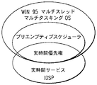
図8は、本発明の改善されたコンピュータシステムに対するマルチメディア拡張モデルの実施例の概略線図である。特に、本発明のIDSPによって提供された実時間サービスが、また、マルチスレッドかつマルチタスキングであるWindows OSの割り込みスケジューラに実時間優先権を供給することが判る。図32及び33は、後に論じられるが、実時間性を与えるためにいかに割り込みを取り扱うかの詳細を示す。図35は、或る実時間サービスの詳細を示す。
【0078】
図9は、本発明の改善されたコンピュータシステムに対するシステム/キャッシュ/仮想メモリモデルの実施例の概略線図である。DSPコアは、データ及び命令を非常に効率的に往き、戻り移動させるキャッシュである。CPUは、データをハードディスクからこのキャッシュへ移動させる。本発明の改善されたPC用キャッシュ動作方式を説明する。
【0079】
図9で、ラン時間中、コードをハードディスク装置(HDDとも称する)から主メモリ112へ取り出す。ラン時間中、コードの断片を主メモリ112から図2のブロック214へ取り出す。ブロック210がDSP及びCPUと独立に、コードを更に図9のDSPメモリ918及びC5xメモリへ移動させる。キャッシュ動作方式は図6bに示されている。図2で、ブロック210はキャッシュ動作方式の部分を行う。図19bで、CPUの休止時間に相当するコードの断片を、いまやブロック300内のDSP側上のメモリを含むように拡張されているCPU内の仮想空間を通して、ページする。このようにして、OSを使用して仮想メモリを物理メモリに翻訳する。図9で、DARAMは2重アクセススタティックRAM、SARAMは単一アクセススタティックRAMである。
【0080】
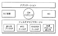
図10は、本発明の改善されたコンピュータシステムに採用されることがあるMPEG再生フィルタグラフモデルの実施例の概略ブロック図である。図10でユーザがソフトウェアオブジェクトをクリックオンすると、Windowsは、ダイナミックにメモリを配分しかつオブジェクトリンキング埋込み(object linking embedding、以下、OLEと称する)をランする。MPEGは、層から層式の代わりにオブジェクトからオブジェクト式で働く。送り手は、伸張するために画像捕獲データを含むことがある。
【0081】
図11は、本発明の改善されたコンピュータシステムに対する仮想I/Oハードウェア−PCIDMA及びマルチメディア実時間割り込みハンドラモデルの実施例の概略ブロック図である。図11で、システムは、実時間に割り込みを遮る。DSP空間は、主メモリ112内に実際目的のために在駐する外部スタティックRAM(以下、SRAMと称する)である。それゆえ、送り手空間、受け手空間、及びDSP空間は、全て同じ空間内に包含される。このようにして、そうでなければWindowsシステムに配分することのできないリソースをダイナミックに得る。遺産コードは、システム100上で互換的にWindowsの下で有利にランする。アプリケーション(APPとも称する)は主メモリの部分を使用し、これらをPCIバス散乱−収集DMAコントローラを示されたブロックへ効果的に分解する。
【0082】
図12は、本発明の改善されたコンピュータシステムに対するフレーム内のCPU及びIDSPによる並列処理の概略ブロック図である。図12で、フレームが与えられると、ホストCPUは、処理を全て実行しかつ時間帯1204内の多数のスロットを独占しなけばならない。有利上、DSPとCPUの組合わせが2つの時間帯1210と1212を提供し、ここでDSPは時間帯1210内のフレームを処理し、かつ離散余弦変換器(以下、DCTと称する)がCPU時間帯1212内の2つの短いタイムスロットになる。
【0083】
それゆえ、比較的中位の性能のDSPが主要な画像処理を行う充分なリソースを有するが、これはこのDSPがその信号処理タスクに専用されるためである。LAN、モデム、及び他のアプリケーションは画像処理と時分割されるが、しかし図12の分析点と無関係な他の時間間隔中においてである。
【0084】
図13は、本発明の改善されたコンピュータシステムが採用することがあるMPEGエンコーダ1300の簡単化ブロック図である。特に、入来ビデオ画像をブロック1301内でリオーダ(reorder)し、次いで運動推定ブロック1303に供給して画像のどのエリアが変化しているかを判定する。運動推定ブロック1303からの出力を画像/記憶予測ブロック1305、出力マルチプレクサ1307、及び加算器1309に供給する。画像/記憶予測ブロック1305からの出力を加算器1311及び加算器1309に供給する。加算器1309はDCTブロック1313の入力へ供給し、ブロック1313は出力を量子化ブロック1315へ供給する。量子化ブロック1315は、出力を可変長エンコーダ1317及び逆量子化ブロック1319へ供給する。逆量子化ブロック1319は、出力を逆DCTブロック1321に供給し、後者は出力を加算器1311に供給する。可変長エンコーダブロック1317は、出力をマルチプレクサ1307に供給し、このマルチプレクサは出力をバッファ1323に供給し、このバッファはコード化ビデオデータを出力する。このようなエンコーダは、ハードウェア内又はソフトウェア内で実現される。
【0085】
図14は、本発明の改善されたコンピュータシステムが採用することがあるMPEGデコーダ1400の簡単化ブロック図である。入来コード化ビデオを入力バッファ1401に記憶し、このバッファはデマルチプレクサ1403へ出力し、このデマルチプレクサは画像記憶/予測ブロック1405及び可変長デコーダ1409へ出力する。画像記憶/予測ブロック1405は加算器1407へ出力する。可変長デコーダ1409は逆量子化ブロック1411へ出力し、このブロック1411は量子化ブロックステップをデマルチプレクサ1403から供給される。逆量子化ブロック1411は逆DCTブロック1413へ出力し、後者は加算器1407へ出力する。加算器1407は画像記憶/予測ブロック1405及び画像リオーダブロック1415へ出力し、ブロック1415はデコードしたビデオ画像を出力する。
【0086】
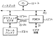
図15は、CPUとしてP5プロセッサを採用することがある本発明のノートブックコンピュータに対するビデオ解決の実施例の簡単化ブロック図である。図15で、システムは、図4aに示されたのと同じように、PCMCIA標準、改正2.1を用いて働く。
【0087】
ZVは、エキストラフレームバッファを要せずフレームバッファ内に収容されるビデオ入力リソースに適合する。PCIは、等時的ではなく、バーストされかつ割り込まれ、したがってビデオには極めて不利である。本発明によれば、フレームバッファに接続された専用バックドア私設高速バスZVによって等時性能力が付けられる。ブロックを図4のチップ420又は460内に一括にリンクするのが、加速バスである。
【0088】
図16は、CPUとしてP5プロセッサを採用することがある本発明のデスクトップコンピュータに対するビデオ解決の実施例の簡単化ブロック図である。図16は、PCMCIA又はカードバスを用いないデスクトップPCを示す。それゆえ、MPEGビデオを再生中、CPUはビデオデコード機能を遂行するのに対して、DSPはオーディオデコード機能を遂行するか、又はこれの反対である。もしデータがCD ROMから到来するのであるならば、システム同期はCPUによって遂行される。もしデータが外部カメラ1394又は他の外部画像捕獲システムから来るならば、DSPがシステム同期を遂行するが、それはこのデータがまずDSPに到来するためである。このようにして、このシステム及び方法は、どのプロセッサがシステム同期を遂行するべきかの問題を有利に解決する。
【0089】
図17は、本発明の改善されたコンピュータシステムに対するアプリケーションパイプラインの簡単化ブロック図である。図17で、単一プロセッサは、たとえスーパースカラプロセッサであっても、アプリケーションレベルでパイプラインすることはできない。これは、パイプラインプロセッサのハードウェアパイプラインと明確に異なる。意味する所は、アプリケーションをパイプラインするために同じ時間にパイプラインの異なる部分を実行すると云うことである。
【0090】
ステージが、アプリケーションの性質によって確立される。例えば、DSPがビデオのNフレームを伸張するのに対して、x86CPUが同時にフレームN−1についてプロセッサデータをスクリーンへ出力し、次いで、このサイクルをパイプラインに関係した仕方で繰り返す。DSPは、また、フィルタリング、スケーリング、及びカラー変換を遂行するのに対して、CPUはデータを入力又はデータを出力する。
【0091】
図18は、本発明による改善されたコンピュータシステムに対するハードウェアアーキテクチャの他の実施例のシステムレベルを示すブロック図である。図18は、図1の簡単化ブロック図の代替配置を示す。図18は、PCIバスを使用しかつプラグインPCIカード1820用スロット1810を有するPDCを示す。プラグインPCIカード1820は、図3又は図4aに示されたように、PCIインタフェース(I/F)1822、DSP1824、及び関連コーデック1826を含む。その他はいずれも標準PCハードウェアである。ハードディスク装置1830は、標準PCハードウェアの部分である。コーデック1826は、オーディオ機能を取り扱う。
【0092】
PCIカード1820は、PCIマスタ及びPCIスレーブの両方である。ホストCPUは、スレーブモードでPCI構成レジスタ及び主メモリポインタレジスタにアクセスすることができる。マスタモードで、DSPは、散乱−収集DMAを使用してプログラムコード及びデータを取り出し、かつ主メモリに記憶することができる。
【0093】
図19bは、図1の改善されたコンピュータシステムの好適実施例の更に詳細な電気回路図(部分的に概略図、部分的にブロック図)である。図19bは、図3に類似しているが、しかし更にDSP1950及び関連メモリ1952、1954の詳細を示す。加えて、コーデックチップ1956ばかりでなく、チップ300(図3に示されている)、スピーカ1962、及びマイクロホン1960へのその接続を示す。図38から図44は、この実施例における一配置の詳細を示す。
【0094】
DSP1950は、CPUと独立にランする。CPUは、PCIカードがスレーブのとき、リセットの後初期化コードをDSPへダウンロードし、そこで、DSPは独立する。CPUは、PCI I/O空間レジスタ308内のSTARTビットをセットすることによってDSPを始動させることができる。STARTビットは、DSPにとって割り込みであり、DSPにコード実行を開始させる。DSPは、コード実行を終了するまでPCIマスタとして独立に実施する。DSPアルゴリズムが終了したとき、DONEビットがPCI状態語(StatusWord)308内にセットされかつCPUへの割り込みがPCIバス上に発生される。
【0095】
CPUは、主メモリにポインタアドレスを供給する。必要な3つのアドレスは、プログラム空間についてのDSPの128Kバイトに対するベースアドレス、読び出し空間(送り手)についての128Kバイトに対するアドレス、及び書き込み空間(受け手)についての128Kバイトに対するアドレスである。アプリケーションに従って、これらはメモリの異なるエリアを指摘する、又はメモリの同じエリアを指摘する。CPUは、DSPに対するSTARTビットを有するレジスタ308に書き込むことによってDSPを制御する。DSPは、このビットを割り込みとして使用する。この割り込みは、DSPにロードされたアルゴリズムを開始させるか、又はホストがコマンドをDSPに送ったことを表示する。
【0096】
レジスタ308内の他のビットは、DSPリセットビットである。このビットは、DSPのリセットピンへ送られる。このビットは、現行DSPタスクを打ち切らせて、DSPをブートロード順序で開始させる。新タスクをDSPにロードするために、DSPをリセットするか(これはブートロードするために追加の時間を要する)又はMASTER ABORTビットをホスト制御されるレジスタ308にセットするかのどちらかをできる。MASTER ABORTビットがセットされると、割り込みがDSPに発生されて、これが初めにロードされたブートコードを実行させる。このブートコードは、RCI I/O空間メモリプログラム空間ポインタによって現在指摘されているホスト主メモリからDSPタスクをロードする。DSPは、PCI I/O空間CMD/STATUSレジスタ308内にEVENTビットをセットすることによってそのタスクが終了したことを表示しかつPCI割り込みを発生する(タスクを完了する前にビットがまたセットされて、DSPが働いていることを表示する)。
【0097】
PCIアプリケーションカードDSPアーキテクチャは、初期的には無メモリである。これは、コストを可能な限り低く押さえる必要のあるシステム製造業者の関心を引く。しかしながら、このアーキテクチャは、メモリ1952、1954で示されたような、外部プログラム空間メモリ又は外部データ空間メモリを追加することを妨げない。もしDSPアプリケーションソフトウェアが逐次8ビットアクセスを行う時間及びオーバヘッドを提供できるならば、データメモリを実現するために16ビット2RAMチップメモリシステムの代わりに1つの8ビット幅外部RAMを使用してもよい。無メモリシステムを達成するために、DSPの内部メモリをプログラム空間とデータ空間とに分割することになる。もしプログラムが内部メモリに適合するには大き過ぎるならば、コードを必要に応じて主メモリからPCIバス上へ取り出さなければならない。生データが主メモリから取り出され、かつDSP動作の結果のデータを主メモリに帰されることになる。
【0098】
外部メモリがない場合は、DSP内へのコードを実行化可能にするただ1つの方法は、DSPをリセットしかつROMをベースにしたブートローダを使用して主メモリからの小さい初期化プログラムをロードすることである。DSPのブートローダ版(「BDSP」)を以下の説明に使用する。このDSPは、どの型式のブートローディングが起こるかを決定するために、リセットされたグローバルメモリアドレスFFFFを読み出す。4つの最下位ビット内の1100の値は、ハンドシェーキング用XF信号及びベーシックI/O(以下、BIOと称する)信号を使用する16ビット並列I/Oロードを表示する。BIOが低のとき、データバスが駆動される。ブートロードが完了した後、BIOはDSPデータバス上のバス衝突を防止するために高のままでなければならない。
【0099】
16ビット語をI/Oブートモードを介してロードすることによって、CPUがベーシック主メモリ初期化プログラムをDSPに敏速にロードすることができる。DSPはリセット状態になり、それであるからDSPはスレーブとしてPCIバストランザクションに応答することができるだけである。PCIホストは、DSPにロードされている初期化プログラム値を制御することになる。これが、初期化プログラムをソフトウェアで修正できるようにする。このルーチンがロードされた後、DSPはリセットを解かれ、それであるからDSPは初期化プログラムを実行することができる(DSPのBIO信号をFIFO状態信号で駆動できるようにするためBIO選択ビットをまたセットしなければならない)。初期化プログラムは、PCIバスマスタとして働きかつ主メモリに入って実際DSPアプリケーションソフトウェアを取り出す。初期化プログラムのみをブートロードすることによって、DSP PCIバスマスタが実際DSPアプリケーションコードのローディングを制御することができる。
【0100】
もしDSPアプリケーションソフトウェアがDSP内部メモリ内に全体として適合できないならば、より多くのコードをスワップインする必要がある。このコードは、主メモリから取り出される。多くのコードを取り出すために、DSPアプリケーションはBLDP(Block Load Program to Data)命令を遂行することがあり、これはグローバル(Global)空間データを取り出し、それをプログラム空間へ移動させる。もしグローバルデータ(Global Data)空間が外部メモリであると指定されかつプログラム空間が内部メモリであると指定されるならば、コードを移動させるために必要な外部アクセスをBDSPが行う。DSPは外部世界へのグローバルデータ空間取り出しを行いつつあるので、そのアプリケーションソフトウェアは、PCIインタフェースにDSPコードがバス上に取り出されつつあり、データではないことを告げる機構を必要とする。I/Oポートレジスタビットが、取り出されつつあるのはプログラム空間コードか、送り手データか、受け手データか、又はDSP決定したデータかどうかを表示するために使用されることになる。I/Oポートレジスタビットは、リセットされているプログラム空間をアクセスするようにセットされる。
【0101】
アプリケーションコード内に持ち込まれて使用された最初にブートロードされたコードは、好適には、メモリ内に維持されているものとする。これは、CPUにこのアプリケーションをリロードするように割り込みを強制することによってDSP動作を打ち切らせる。もしこのコードが喪失するならば、CPUはDSPを制御しなくなり、かつプログラムコードをリロードするためにDSPをリセットしなければならない。DSPアプリケーションソフトウェアは、データを外部メモリから内部メモリへ転送しかつBLDD(Block Load Data to Data)コマンドによってこれを復帰させることができる。
【0102】
PCIインタフェースは、PCIマスタ及びPCIスレーブの両方である。このインタフェースは、CPUが構成空間にアクセスすることができるようにスレーブであることを要する。CPUは、DSPへの或る制御を実行しかつ主メモリポインタを組み立てるためにメモリ空間又はI/O空間のどちらかにアクセスすることができる。DSPは、コード及びデータについて主メモリをアクセスするためにPCIマスタであることになる。また、PCIインタフェースに含まれてFIFO310がある。このFIFOは、好適には、データの64バイトを保持する。BDSPは16ビット外部データバスを有するので、PCIバスとBDSPバスとの間のFIFOは、DSPプログラムとデータを32ビットから16ビットに変換しなければならない。各主メモリ場所に2つの命令又は2つのデータ語を詰めることによって、所与のアプリケーションに要求されるPCIバスの数を2分の1に減少することができる。
【0103】
PCI標準によって要求される構成レジスタは、PCI I/O空間及びメモリアドレス空間内のエリヤを0及び1で以て指定するために使用される。要求される限りのPCI空間は5つの倍語である。アドレス空間は2のべきで要求されるので、8アドレスを確保しなければならない。必要とされるこれら5つの倍語より上のレジスタは使用されず、もし読み出されるならば、0を返すことになる。これら5つの倍語は、プログラム空間ポインタ、データ空間ポインタ、DSPコマンド、DSP状態語、及びBDSPをブートロードするためのI/Oポートに使用される。
【0104】
PCIホストは、PCI I/O空間レジスタ308を書き込む。DSPは、これらのレジスタによって制御される。構成レジスタ内のベースアドレス0及び1は、このチップが応答するPCI空間のエリアを指摘する。両ベースアドレスが同じ空間を指摘するが、しかしベースアドレス0はI/O空間として構成される。ベースアドレス1は、メモリ空間として構成される。これによって、メモリベースシステム又はI/Oベースシステムのいずれかを設計するシステム設計者にとって融通性が増すようになる。DSPと通信しかつこれを制御するために、20バイトが必要である。32バイトがPCI構成レジスタ内に確保されている。レジスタ0x64から0x1Fが確保されることになりかつ0だけを返す。それらのアドレスは、ベースアドレス+0x0からベースアドレス+0x13である。これらのレジスタによって、CPUが、主メモリのどの部分をDSPメモリに対して使用するべきかを決定できるばかりでなく、DSPの状態を開始、停止、及び監視できるようになる。主メモリプログラム(及びデータ)空間レジスタの下位12ビットが確保される。これによって、プログラム及びデータ空間が4K境界内に再配置される。
【0105】
DSPアルゴリズムが終了すると、状態語内のEVENT INTERRUPTビットがセットされる。このビットがセットされると、割り込みがPCIバスを通してアプリケーションソフトウェアに対して発生される。この割り込みはDSPソフトウェアによって制御されるので、割り込み許可(enable)はハードウェア内で実現されない。
【0106】
DSPハードウェア制御語は、DSPハードウェアの動作を直接制御する。その最下位4ビットは、リトライカウンタ(Retry Couter)ビットである。リトライカウンタビットは、もしPCIマクロ機能がPCIトランザクションを初期的に失敗するならば、この機能にそれをリトライさせる。この値は、上掲の機能にいつまでもリトライをさせることになる0000にリセットされる。この値を、1から15リトライの間にするように変化させることができる。もしトランザクションが遂行されないためにリトライカウンタがランしなくなるならば、MISC CTRLレジスタ内のリトライカウンタ期限切れ(RetryCounter Expired)ビットがセットされる。この状態は、ホストに利用可能である。
【0107】
DSPインタフェースASICは、PCIインタフェース、PCI FIFO、DSP(接続デバイス)インタフェース、及びCODECインタフェースからなる。この調査研究は、BDSPが離散チップであることを必要とする。
【0108】
DSPは、利用可能な5ユーザ割り込みを有する。これらの割り込みの1つは、マスク不可能であり、4つはマスク可能である。CODECインタフェースは、3割り込みを必要とし、PCIインタフェースレジスタは2割り込み及びRESETピンを必要とする。これらの割り込みは、次のように使用される。すなわち、NMI− マスタ打ち切り(PCIホストからDSPへ)、INT1−CDRQ(コーデックから)、INT2−PDQR(コーデックから)、INT3−IRQ/IRQ2(コーデック1とコーデック2から)、及びINT4−コマンド(PCIホストからDSPへ)。コンマンド割り込みは最低優先権であるが、これはRESETピンから出るのとDSPアルゴリズムに応答するのとの間になされる充分なハウスキーピングがあるから問題はない。マスタ打ち切り割り込みは、最高優先権であり、DSPにその初めのDSPコードをリロードさせるのに使用される。割り込み1、2、及び3は、コーデックによって発生される。もし第2コーデックがユーザによって必要とされるならば、IRQ割り込みを共用することができる。IRQ信号とIRQ2信号が一緒にゲートされてDSPに対する1割り込みを生じる。IRQ信号、CDRQ信号、及びPDRQ信号は、ASICによって反転される。ユーザによって供給されるIRQ2信号は、低で活性でなければならない。
【0109】
DSPは、メモリマップI/Oポートにアクセスし、このポートは動作マスタリング用PCIマクロを制御するために使用される。
【0110】
CODECレジスタは、DSPによってPCIアプリケーションボード上の離散CODRECと通信するために使用される。FIFO状態は、I/OポートでDSPによって利用可能である。このASIC又は将来のASICの改正によっては、FIFOが異なった寸法を持つこともある。性能を同調させるために、どんな寸法のFIFOと共にDSPが働かなくてはならないかを知ることは、DSPを助援するであろう。FIFO寸法レジスタは、FIFOが保持することのできる語の最大数を表示する。転送するDSP語の数は、他のI/Oポートに書き込まれる。この値は、転送するバイトの数を得るためにハードウェアでは2倍される。転送することのできる語の最大数は、32768(65536バイト)である。これは、レジスタ0x59の最上位ビットを使用することができないことを意味する。もし1がそのビットに書き込まれるならば、それは無視される。
【0111】
PCIアドレスオフセット(0x58)はDSP空間内のアドレスであって、PCI空間内に転送されて、データをホストへ又はこれから転送するのに使用される。DSPは、DSPポインタをPCI加算(Adder)ポインタレジスタに書き込むことによってホスト主メモリをアクセスし、PCI加算ポインタレジスタは2DSP語を取り上げかつ32ビットPCIポインタを作る。これは、もしDSPが散乱−収集テーブルにデータベースを有する主メモリ内の位置を計算することを必要とするならば、有効である。PCI制御レジスタ内のPCIアドレス空間選択ビットは、PCIバストランザクションが開始されたとき、PCII/O空間に書き込まれたDSPポインタ又はPCIポインタを使用するかどうかを決定する。
【0112】
コーデック状態/モードレジスタ(0x5F)は、全16ビットについて読み出し可能である。その下位8ビットだけが書込み可能である(上位8ビットは読み出されるだけ)、BIO選択は、DSP BIO入力に接続されるFIFO状態又はユーザ信号を融通性選択を可能にする。状態信号の全て、したがって、BIOは、高で活性である。
【0113】
DSPは、PCI ASIC上の64バイトFIFOを通してPCIバスからの又はこれへの読み出し及び書込みを遂行する。PCIのFIFOは、PCIクロックに同期する2並列16語FIFOとして構成される。DSP制御信号は、DSPのCLKOUT1信号に同期する。プロセッサをクロックするのに2つのオプションが用意されている。第1オプションは、DSPをPCIクロック速度(最高33MHz)で内部的にランさせるためにPCIクロックを2で分周しかつDSPのCLKIN2入力を使用する(これはCLKIN2信号を2で倍周することになる)。この結果、PCICLK信号がCLKOUT1信号と同じ周波数になる状況を生じる。しかしながら、CLKOUT1信号が最大約270度移相されることがある。クロック分周電子回路を通しての遅延及びDSPの位相ロックループ(以下、PLLと称する)を通しての移相は、最長25nsの総合遅延を起こすこともある。第2オプションは、PCICLK信号を1で分周しかつDSPの1による分周入力オプションを使用する(DSPはこのモードを支持しない)ことである。最終結果は、PCICLK信号が依然CLKOUT1信号と同じ周波数であるが、しかしその位相は異なると云うことであろう。
【0114】
DSPのRDz(読み出し許可−−低で活性)信号及びWEz(書き込み許可−−低で活性)信号が、FIFO読み出しパルス及び書き込みパルスを発生するために使用される。DSPによる読み出しを、クロック遅延を考慮することを保証するために、少なくとも3ソフトウェア待機状態で以て遂行しなければならない。
【0115】
クロック遅延を考慮に入れる保証をするために、DSPによる書き込みを少なくとも2ソフトウェア待機状態で以て遂行しなければならない。
【0116】
DSPは、FIFOから到来する及びこれへ行くデータを管理する。このデータ流は、FIFOをオーバーランかつアンダラン(underun)させない限りDSPにトランスペアレントであり得ない[DSPはPCIバスをアウトラン(outrun)しかつFIFOをオーバランすることもあり得る]。DSPにリソースを最善に使用させるために、いつFIFOが読み出すデータを有する又はFIFOが書き込み中いつ空になったかをDSPに告げるためにフラグとしてBIO信号を使用することになっている。DSPからの書き込みを遂行する2つに方法がある。第1の方法は、FIFOが(読み出し又は書き込み前に)空になるまで待機し、次いでFIFOを満たす数の語を読み出す又は書き込むことである。これは、現行のハードウェア構成では32語を扱うことになり、FIFOをオーバラン又はアンダランしないように保証する。32語を読み出し又は書き込んだ後、DSPはBIO信号をループに載せ(これはFIFOが他の12語を受ける用意を整えたことを表示する)かつ他の32語を読み出し又は書き込みすることができる。
【0117】
第2の方法は、12語より大きいデータのブロックを転送させることである。この方法は、BIO信号を使用するが、しかしDSPはFIFOへの毎読み出し又は書き込みの前にBIO信号をループに載せる。これらの動作に関してBIO信号を介してFIFO状態を表示するために、半空及び半満フラグを使用することができる。DSPは、そのI/O空間を使用して、PCIトランザクションを開始させるために制御レジスタ内にビットをセットする。その制御レジスタパラメータは、PCIアドレス空間選択ビット、FIFOリセットビット、PCIマクロビット、DSP状態ビット、開始ビット、及びBIO選択ビットである。トランザクションが開始する前にFIFOの状態を検査するために状態レジスタがまた必要である。PCIバストランザクションを開始させるのに必要なパラメータは、DSPアドレス(これはPCI主メモリアドレスに翻訳される)、転送する語の数(ハードウェアは語の数をバイトの数へ変換する)、及び方向である。
【0118】
2語だけがPCIバスを通して転送されるとき、信号データ位相転送が起こる。これらの2語は1つの32ビットトランザクションを満たすだけである。PCIマクロは、PCIプロトコルを正しく取り扱うためにこの特別な状況を知っている必要がある。DSPによって書き込まれた値(語の数)は、バイトの数を得るために2倍され、それであるからバイトの最少数は2である。実際に転送するべきバイトの数は4ある。もし4バイト未満が転送されるならば、DSPはPCIバスバイト許可ビットを変化させなければならないか、又はPCIデータ位相の4バイトのうちの2つが有効でないことになる。方向ビットは、これがFIFOの入力の送り手内の決定因子であるので、重要である。方向ビットは、DSPがFIFOに書き込むとき自動的にセットされる(これは、ビットをセットし、FIFOを書込み、次いでトランザクショを開始させなければならないことを防止する)。PCIバスからの読み出しの際、方向ビットは、トランザクションを開始させるレジスタへの書込みによってセットされる。BIO信号は、BIO選択レジスタの値によって選択される。この値を、読み出し動作と書き込み動作との間に変化がある毎に変化させなければならない。
【0119】
これらのパラメータがインタフェースASICに書き込まれた後に、開始ビットがDSPによって書き込まれたときPCI転送が開始される。DSP順序の例は次のとおりである。すなわち、
【0120】
DSP読み出し順序
1. 転送されて来るデータのアドレスを書き込め。
2. 転送する語の数(≧2)を書き込め。
3. 終了(DONE)ビット(それをクリアせよ)、 ワーキングビット(それをセットせよ)、転送の方向(0=読み出し)、BIO選択、及び開始(START)ビットを書き込め。
【0121】
いったん開始ビットがセットされると、ハードウェアは、すなわち、
3.1 PCIバスが自由になる(P2CDGNTCUPL信号が不活性へ移行する)のを待機せよ。
3.2 CD2PREQCULPL信号及びCD2PGNTCUPL信号をセットするためにレジスタに書き込め。
3.3 P2CDGNTCUPL信号が活性へ移行するのを待機せよ。
3.4 (他のトランザクションを防止するために)CD2PMSTCUPL信号をセットするためにレジスタに書き込め。
3.5 新アドレス、バイトの数、方向、及び多相状態をマクロへストローブせよ。
3.6 FIFOを満す動作を開始せよ。
4. FIFOが空でないことをマクロが表示するのを待機せよ。(この状態をBIOとしてDSPにもたらせ)。
5. FIFOから読み出せ。読み出しを2サイクル/1待機状態命令をで以てFIFOから行うことができる。これらの待機状態は、ソフトウェア待機状態である。FIFO読み出しパルスは、DSP読み出し信号によって発生される。もしFIFOがデータを持たないならば、BIOはセットされず、動作は延期される(これについて、内部時間切れを使用しなければならないことがある)。BIO信号を使用することによって、DSPはデータを待機する。3.にループバックして、完成まで繰り返せ。PCI割り込みの発生が完了するとき、DONEビットをオプショナルにセットすることができる。
【0122】
もしPCIバススレーブが最後の2データ位相中待機状態なしでランできるならば、PCIマクロはFIFOを満たすことになる。もし最後のデータ位相になんらの待機状態がないならば、FIFOは最後の語を書き込まれないことになる。FIFOは、FIFO Full−1倍語を内部に有することになる。
【0123】
DSP書き込み順序
1. FIFOが空であることをマクロが表示するのを待機せよ。(この状態をBIOとしてDSP内に持たらせ。)
2. FIFOに書き込め。書き込みを3サイクル/1待機状態命令で以てFIFOに行うことができる。これらの待機状態は、ソフトウェア待機状態である。FIFO書き込みパルスは、DSP書き込み信号によって発生される。
3. 転送されるデータのアドレスを書き込め。
4. 転送する語の数(この場合、32)を書き込め。
5. 終了(DONE)ビット(それをリセットせよ)、ワーキングビット(それをセットせよ)、BIO選択、及び開始ビットを書き込め。
【0124】
いったん開始ビットがセットされると、ハードウェアは、すなわち、
5.1 PCIバスが自由になる(P2CDGNTCUPL信号が不活性へ移行する)のを待機せよ。
5.2 CD2PREQCUPL信号及びCD2PGNTCUPL信号をセットするためにレジスタに書き込め。
5.3 P2CDGNTCUPL信号が活性へ移行するのを待機せよ。
5.4 (他のトランザクションを防止するために)CD2PMSTCUPL信号をセットするためにレジスタに書き込め。
5.5 新アドレス、バイトの数、方向、及び多相状態をマクロへストローブせよ。
5.6 FIFOが空であることをDSPに警告せよ(BIO信号を使用せよ)。3.にループバックして完成まで繰り返せ。
【0125】
DSPが主メモリにアクセスするとき、DSPの16ビット語指向アドレスを32ビットバイト指向アドレスに翻訳しなければならない。この翻訳の部分は、DSPの16ビットを1ビット左へシフトさせる(2を乗じる)ことを要求する。これは、メモリ空間の64K語をアドレス指定する代わりに、DSPがPCIホスト主メモリの128Kバイトをアクセスすることが実際にできることを意味する。PCI仕様は、直線アドレス指定(アドレスがバースト転送中直線的に増分する)を使用することを望むPCIイニシエータがアドレスの2最下位ビットを00として残すことを要求する。これは、主メモリからの全ての取り出しを奇数アドレス(最下位ビットが0)で以て開始しなければならないと云う制約をDSPソフトウェアに課する。主メモリ内のアプリケーションに融通性持たせるために、DSPデータ空間及び命令空間は4K境界上で再配置可能であることになる。
【0126】
PCIバスは、選択可能幅バスである。どんな4バイト許可信号も、このバス上の4バイトのどれか又は全てが有効データであることを、活性で以て表示することができる。DSPは16ビットバスを有し、このバスは毎転送の際有効データの16ビットを有するものと仮定する。DSPがPCIバス上のイニシエータである間、全てのバイト許可信号は活性である(全てのデータは32ビット)。PCIバスとDSPバスとの間で転送するために、並列な2つの16ビットがあってPCIデータを捕獲する。DSPは、いくつかのFIFOの出力を多重化(mux)して16ビット語を得る。多重化はDSPの最下位ビットによって制御される。アドレスビット0上の0は、最下位語FIFOを選択しかつアドレスビット0上の1は最上位語FIFOを選択する。
【0127】
ステレオオーディオコーデック1956は、ISAバスインタフェースを備える8ビットデバイスである。このコーデックは、DSPのデータバスから分離されているデータバスに接続される。DSPは、I/O空間レジスタを経由してこのコーデックにアクセスする。DSPが低速ISAインタフェースを待機するのに拘束されるのを防止するために、ASIC316がDSPからの及びこれへの実際読み出し及び書き出しを制御するステートマシンを実現する。
【0128】
コーデックを統制するこのステートマシンは、DSP I/Oアドレス空間におけるコーデック状態/モード(CODEC Statue/Mode)レジスタを介して制御される。ステートマシンは、1が開始ビットに書き込まれるとき開始する。読み出し又は書き込みが要求されるかどうか、及びPIOアクセス又はDMAアクセスが要求されるか否かに従って、ステートマシンは適当なプロトコルに従い、かつそれらのバイトをI/O空間レジスタに書き込むか又はコーデックの内容を読み出してそれらのレジスタ内に入れるかする。BYTE XFER COUNTビットは、DMA動作中いくつのバイトが転送されるかを決定する(ビット1から4)。ADDR SELビットは、PIOアクセス中どのアドレスに最下位バイトが書き込まれるかを決定する(ビット0から3)。コーデックステートマシンが完了すると、コーデック状態ビットDONEがセットされる。このビットは、ステートマシンが開始するときクリアされる。このビットは、DSPのみに対する情報のために提供される。
【0129】
PCIカードユーザは、DSPのプログラム空間内及びデータ空間内の外部メモリを含むオプションを有する。このメモリ(容易な設置及び除去のためにソケット接続される)によって、DSPアルゴリズムは、ホスト主メモリへのアクセスの利点を活かしてコードを再書き込みできるようになるまで、その現行形式を維持することができるようになる。データ空間は、ローカルデータをホスト主メモリから分離して維持するために利用可能である。グローバルメモリは、ホストシステムへのインタフェースとして指定される。このインタフェースは、グローバルメモリ空間内に在駐するFIFOを経由することになる。このメモリは、READY信号の代わりにソフトウェア待機状態を使用してアクセスされる。
【0130】
ブートロードプロセスは、グローバルメモリ位置0xFFFF及びメモリマップI/Oポート50hを使用する。この位置は、もしPCI I/O空間レジスタ内のBIOビット(DSPコマンド語 −− ビット3)が高にセットされるならば、グローバルメモリ内で利用可能である。もしBIOが低にセットされるならば、位置0xFFFFからの読み出しの結果、ブートロードデータとグローバルメモリデータとの間にバス衝突が起こる。もしユーザがグローバルメモリを使用しなければならないならば、DSPからASICへのBR#信号がユーザアドレスデコード信号で以てゲートされて、ユーザのグローバルメモリアクセスの際にASICのFIFOが活性になるのを防止する。
【0131】
パワーオンの際に実行されるPC BIOシステム(以下、BIOSと称する)ソフトウェアは、どの種のPCIカードがシステムに設置されているかを発見する責務を負う。このソフトウェアは、云わゆるパワーオンセルフテスト(以下、POSTと称する)コードであり、かつPCIアプリケーションの総称的初期化を遂行する責務を負う。初期化を完了した後、カードを主メモリに挿入し、自己のプログラムコードを取り出す。
【0132】
いったんPCがパワーアップされると、DSPは、ホストDSPドライバがDSPのリセットを解くまで、リセット状態に保持される。この点で、ドライバは、PCI I/O空間コマンド語(COMMAND WORD)レジスタに書込みしてDSPのリセットを解く。そこで、CPUがBDSPをブートロードする。このデバイスドライバは、XFをセットするためにBDSPを捜すことによってPCI I/O空間ブートロードデータ(BOOTLOAD DATA)レジスタを経由して16ビット語をDSPにダウンロードし、次いで、有効データがブートロードデータレジスタに書き込まれた後、(コマンド語レジスタ内に)BIOをセットする。これは、PCI ASIC内に又はアプリケーションカード上に追加のハードウェアを必要としない。これは、ホストDSPドライバに関していくらかのオーバヘッドを起こす。これは、また、ブートロードコードをソフトウェア内で変化させることができるので、最も融通性に富む調査研究である。いったんDSPが初期化されると、DSPはCPUがレジスタに書き込みかつCOMMANDビットをセットするのを待機する。COMMANDビットは、DSPへの割り込みを発生しかつDSPに実行を開始させる。この初期DSPコードのなすべき第1のことの1つは、データメモリの存在を検査することである。もしデータメモリが発見されるならば、そのメモリが8ビット幅か16ビット幅かどうか判定しなければならない。DSPグローバルメモリの存在は、DSPアプリケーションがPCIカードにアクセスするPCIバスを経由することを要せずPCIカード上の高速メモリにデータの最大64K語(又はバイト)までを記憶する機会を得ることを意味する。
【0133】
図20は、本発明の改善されたコンピュータシステムに対するメモリ分配及びロッキングモデルの概略ブロック図である。図20に示されたメモリ配分及びロッキングは、図11に示されたものに相当する。DSP空間に対するポインタがあることがDSPソフトウェアを通して知られている。トランザクション毎に、何処に送り手及び受け手テーブルあるかがまた知られている。図20は、メモリアーキテクチャに対するディレクトリを提供する。図11は、単一送り手空間及び連続受け手空間を表す。Windows95では、これは仮想空間について云えるが、物理アドレスは全空間にわたって散乱している。それゆえ、DSPによる散乱−収集バスマスタリングなる用語がある。
【0134】
図21は、本発明の改善されたコンピュータシステムに対する送り手及び受け手データDMA転送テーブルモデルの概観ブロック図である。図21で、各ブロック2110、2120、2130、2140は、ラン時間にそのアプリケーションに利用されるメモリ112又はメモリ112の部分内の(散乱ロックされた)領域である。その瞬間にディレクトリが組み立てられ、これが領域内の多数の片に分裂する。リンクリストよって、アプリケーションは仮想空間内を飛び回わることができるようになる。ピンポンバッファ2150、2160調査研究が使用される。このCPUに巧く継がるCPUにとって、受け手が送り手になる。
【0135】
図22は、本発明の改善されたコンピュータシステムに対する送り手データDMA転送テーブルモデルの内部構造の概略ブロック図である。図22で、図20と比較して送り手DMA転送テーブルの更に詳細な構造が示されている。
【0136】
図23は、図22の送り手DMA転送テーブルに対する領域リストの詳細である。図24は、本発明の改善されたコンピュータシステムに対する受け手データDMA転送テーブルモデルの内部構造の概略ブロック図である。図25は、図20のプログラマ/データ空間の部分テーブルの更に詳細なブロック図である。図24は、受け手転送テーブル構造の詳細を示す。図25は、図20のプログラマ/データ空間ブロックの詳細を示す。図23は、図22、24、及び25のいずれか1つにおけるリスト領域の詳細を示す。これらの図は、いかにDSP及びホストCPUがローカルメモリ112のような同じメモリ空間を使用する際効に共用しかつ共存するかを示す。
【0137】
図26は、本発明による改善されたコンピュータシステムの他の実施例の電気回路ブロック図である。この実施例の場合、メモリ管理論理、メモリコントローラ、及びメモリ、及びキャッシュは1つのブロックに組み合わせられ、かつローーカルバスを経由してCPUに接続される。ローカルバスは、次に、PCIブリッジに接続され、このブリッジはPCIバスに接続される。更に、ビデオ/グラフィックチップ2614及び画像捕獲/伸張ブロック2618が、2次元及び3次元グラフィック及び本明細書で先に挙げた種々のビデオ画像機能を提供する。
【0138】
図28は、本発明による改善されたコンピュータシステムの他の実施例の電気回路ブロック図である。この実施例の場合、CPUは、そのチップ上に集積されたメモリコントローラ及びPCIブリッジを有し、それゆえメモリ及びPCIバスに直接接続される。集積マルチメディアグラフィックコントローラがPCIバス及びディスプレイに接続される。加えて、2つのオプショナルチップが提供されPCIバスに接続される。1つのチップはDSPを備える周辺I/O COMBO用である。他のチップは、DSPを備えるPCMCIAコントローラ用である。キーボード、マウス、及び並列ポート(以下、PPと称する)が接続されているように、PCのBIOSがI/Oブロックに接続される。ハードディスク装置(以下、HDDと称する)及びフロッピィディスク装置(以下、FDDと称する)ばかりでなく、直列ポート(以下、SPと称する)がDSP部分に接続される。
【0139】
図29は、本発明による改善されたコンピュータシステムの他の実施例の電気回路ブロック図である。図29は、図28に類似しているが、しかし図29の無線LANはPCMCIAコントローラブロックと共に集積化され、1394データ流を含むように高度化されている。
【0140】
図29は、1チップで以て全ての機能が提供されかつ裸ボンド物理層で以てI/Oを提供される実施例を示す。物理層以外のことごとくがPCの部分である。この実施例は、多重周辺電子回路を回避しており、米連邦通信委員会(FCC)の承認を必要とする物理層に重点を置くことができる。回線保護装置(以下、DAAと称する)は、ソフトウェアであり、スピーチコーデックで以て音声注釈する能力を備えている。LANは物理層に重点を置き、DSPは他のLAN機能を仮想化する。コスト低減の終局的ディジタル革新において、物理層以外のことごとくが仮想化され、DSP200はこの革新の中核をなしている。
【0141】
図30は、本発明の改善されたコンピュータシステムに対するアプリケーション/ドライバモデルの実施例の電気回路ブロック図である。VxD環境(以下、VXDEと称する)は、Windowsアプリケーション用DSP関連低レベルサービス、例えば、マルチメディアアプリケーションを提供する。図30に示されたDSPドライバのWindows3.1モデルは、WindowsVxD及びWindowsDLLを含む。Windowsアプリケーションとの又はこれへのDLLインタフェースは、アプリケーションコールバック及びファイルI/Oを遂行し、割り込みを取り扱い、及びVxDとインタフェースする。VxDは、DSPによって使用されることがある物理メモリをロックダウンし及び自由にする責務を負うだけである。
【0142】
DSPドライバDLLが通信する必要のあるWindowsドライバは16ビット又は32ビットであるので、Windows95の下では、上述のモデルはもはや適当でない。16ビットWindowsドライバ及び32ビットWindowsドライバの両方がDSPドライバと通信できるためには、上述のモデルを図31に示したように修正する。
【0143】
図31は、本発明の改善されたコンピュータシステムに対するアプリケーション/ドライバモデルの他の実施例の電気回路ブロック図である。図31に示されたモデルは、WindowsVxD、16ビットWindowsDLL、及び32ビットWindowsDLLを有する。これらのDLLは、WindowsドライバとDSP VxDとの間の通信のためにのみ必要である。しかしながら、このモデルにとって、DSP VxDは、ことごとくに責務を負う、すなわち、DSPとインタフェースし、アプリケーションコールバック及びファイルI/O等を取り扱い、割り込みを遂行し、かつDSP VxD環境と云う名称を与えられている。
【0144】
VXDEは、Windowsアプリケーション用DSP関連低レベルサービス、例えば、マルチメディアアプリケーションを提供する。マルチメディアアプリケーションの場合、これらのサービスには、次が挙げられる。NodeAdvise、NodeAllocate、NodeDestroy、NodeGetAttr、NodeGetData、NodeGetPosition、NodePause、NodePuttData、NodeResetStream、NodeRun、NodeSetAttr、NodeSignalEvent、NodeCovertData、NodeWaitSemaphore、NodeCreatSemaphore、及びNodeDestroySemaphore。
【0145】
Windowsマルチメディアアプリケーションは16ビットDLL又は32ビットDLlを通してVXDEと通信し、VXDEは16ビットの場合はコールバック機能を通して又は32ビットの場合は或る事象信号機構[セマフォー(Semaphore)]を通してWindowsアプリケーションと通信する。VXDEは、DSPのメモリマップポートに書き込むことによってDSPと通信し、DSPはハードウェア割り込みを発生することによってVXDEと通信する。ただし、このハードウェアはVXDEによってVPICDを通して仮想化される。
【0146】
VXDEとの通信を望むどのWindowsアプリケーションにとっても、行う必要のある全ては、16ビットDLL又は32ビットDLL(DSAPI.DLL又はDSPAP32.DLLと称する)と一緒に上に挙げたAPIの集合を使用することである。好適には、16ビットDLLは、呼出し構造にパラメータを入れ、この構造を16ビット側からの呼としてマークし、次いで入口(entry)点を通してVXDEを呼び出す。入口点は、Int 2F機能1684hを使用して位置検出される。他方、32ビットDLLは、DEVICEIOCONTROLインタフェースを通してVXDEを呼び出す。VXDE側では、呼を入口点から受信すると、呼び出し構造のポインタが直線アドレスに翻訳されかつその呼が相当する機能へディスパッチされる。この機能は、どんな型式のポインタでもSELECTOR/OFFSETアドレスから直線アドレスに翻訳し、次いでこの呼を処理する。もし呼がDEVICEIOCONTROLインタフェースから受信されるならば、この呼はなんら翻訳を要せず相当する機能へ直接ディスパッチされる。
【0147】
いつDSPハードウェアが特定タスクを終了したかの通知を望む12ビットWindowsアプリケーションは、それを次によって行うことができる、すなわち、OVERLAPPED構造内に有効事象ハンドルを入れかつポインタをVXDEへ送る。したがって、これは、事象に際してWaitForSigleObjectを呼び出す必要がある。通知を望まないアプリケーションの場合、VXDEを呼び出すとき、OVERLAPPED構造に対するポインタを含むパラメータは零であるとする。
【0148】
いつDSPハードウェアが特定タスクを仕上げたかの報せを望む16ビットWindowsアプリケーションは、コールバック機能を使用することができる。
【0149】
図32及び33は、本発明の改善されたコンピュータシステムに対する図31及び32のアプリケーション/ドライバモデルにおける種々の作用を示す概略ブロック図である。VXDEは、VPICDを通してDSPと通信するために使用されるIRQを仮想化する。指定されたIRQへのどんな割り込みもVXDEへディスパッチされる。割り込みが発生すると、VXDEはまず当該割り込みをクリヤしてどんな将来の割り込みも使用許可し、次いで当該割り込みへのサービスを開始する。もし当該割り込みが16ビットアプリケーションからの呼び出しの結果であるならば、コールバック機能がスケジュール事象(Call_Priority_Event)を通して取り扱われ、この間コールバック機能はVmmサービスSimulate_Far_Callを通して呼び出される。これは、VxDがハードウェア割り込みを処理するとき、それがその呼び出す番号サービスによって制約されるためである。もし割り込みが32ビットアプリケーションからの呼び出しの結果ならば、アプリケーションの通告がやはりスケジューリング事象を通して取り扱われ、ここで、通告はEBX=overlapped.
Internalを用いてWin32サービスvWin32_DIOCCompletionRoutineを呼び出すことによって実現される。
【0150】
図34は、本発明の改善されたコンピュータシステムに対する仮想メモリモデルの実施例の概略ブロック図である。図34のモデルは、いかに全ての通信を直列ポートを通してDSPハードウェアへ再指向させるかを示す。
【0151】
直列ポートを通して通信をDSPハードウェアへ再指向させるために、DSPVxDがサービスの集合をポートドライバ及びポート仮想化VxDに提供する。ポート仮想化VxDがロードされるシステムブート時間に際し、この仮想化VxDは、その実行環境を初期化し、I/Oトラッピングハンドラを設置し、ポートI/Oコンテンションハンドラを設置する、等々、それゆえコンピュータ出力マイクロフィルム(以下、COMと称する)デバイスを仮想化する。
【0152】
ディスクオペレーションシステム(以下、DOSと称する)内のDOSアプリケーションがCOMポートを獲得しようとするとき、そのポートの所有権が実モード仮想メモリ(以下、仮想メモリをVMと称する)に与えられ、そのCOMに関連したIRQがVPICDを通して仮想化され、それだからそのIRGからの割り込みを正しいVMへ反映することができる。COMポートを通すどんな通信も設置されたポートI/Oトラッピングハンドラを通してトラップされ、かつDSP VxDによって提供されるサービスの集合を使用してDSPハンドラへ再指向させられる。
【0153】
システムVMz上でラン中のWindowsアプリケーションがCOMポートを獲得しようとするとき、ポートドライバが、ポート仮想化VxDによって設置されたコンテンションハンドラを呼び出してそのCOMポートの所有権をシステムVMにセットし、かつI/Oトラッピングをターンオフする。COMポートを通るどんな通信もDSP VxDによって提供されるサービスの集合を使用するポートドライバによってDSPハードウェアへリダイレクトさせられる。
【0154】
図35は、本発明の改善されたコンピュータシステムに対する仮想メモリモデルの他の実施例の概略ブロック図である。ハードウェアとのインタフェースがポートドライバ内でのみ起こるように図34のモデルを図35へ変化させることができる。これを行う利点は、ハードウェアを変化させるとき、ポートドライバのみを修正すればよいと云うことである。欠点は、DOSベースアプリケーションに関する追加の遅延である。
【0155】
図36は、本発明による改善されたコンピュータシステムの部分の実施例の電気回路ブロック図である。図36は、グラフィックコントローラのメモリコントローラとの集積化及びこれらのメモリデータバスを通してのメモリの共用を示す。CPUは、メモリコントローラにアドレスを供給し、これを制御し、かつそのホストバス上のデータをデータバッファを経由して受信する。
【0156】
図37は、本発明による改善されたコンピュータシステムの部分の実施例の電気回路ブロック図である。図37は、PCカードソケットとビデオグラフィックアレイ(以下、VGAと称する)コントローラとの間の点対点単方向ビデオバスとしてのVZ(ズームビデオ)の使用を示す。この図は、いかに窓内のTVを低コストPCカードを備える携帯用コンピュータ内で達成することができるかを示す。MPEG又はテレビ会議カードをまたPCMCIAスロットにプラグインすることもできる。
【0157】
図38から44は、本発明による改善されたコンピュータシステムの部分のブレッドボードを示す実施例の電気回路ブロック図である。この実施例は、PCIショートカード定義に適合する多層PCボードであるDC/PC質問カードに変形される。このカードは、ディジタルエリア、アナログエリア、及びブランクエリアを有し、ブランクエリアに子カードを背の低い姿勢で接続することが可能である。アナログエリア用アナログ接地面及びディジタルエリア用ディジタル接地面をコーデックチップに近くして接続するものとする。このボードの端板は、C5xエミュレーションヘッダ(マザーボードに最も近い)、3つのステレオホーンジャック(3.5mm)、2つのRCA844ジャック、及びRJ11ホーンジャック(マザーボードから最も遠い)を収容する。
【0158】
子カード用ヘッダはマザーボード上の2重90度ピンである。子カードは、全体的に背の低いボード用に作られる2重ヘッダソケットを有する。子カード上のI/Oバスを経由して利用可能のアドレス範囲は、ソフトウェア待機状態を異なるアドレス範囲に割り当てるのに融通性を持たせるために分解される。
【0159】
DSPのC5x系列は、どの型式の入力クロック動作方式を使用するか決定する2つの入力ピンを有する。CLLKMD1信号及びCLKD2信号は、4つの異なるロック動作を使用できるようにする(これらの1つは試験用に確保される)。このボード設計は、2つのクロック動作オプションを有する。
【0160】
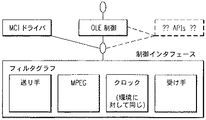
図45は、本発明の改善されたコンピュータシステムに採用されるMPEG再生フィルタグラフモデルの実施例の概略ブロック図である。図10で、ユーザがソフトウェアオブジェクトをクリックオンすると、Windowsアプリケーションは、ダイナミックにメモリを配分しかつOLEをランする。図45の「COMインタフェース」円は、アプリケーションとフィルタグラフマネージャとの間のインタフェースであり、及びMCIブロックはメディアインタフェースを制御する。MPEGは、層から層式の代わりにオブジェクトからオブジェクト式に働く。送り手は、伸張するために画像捕獲データを含むことがある。
【0161】
図46は、本発明による改善されたコンピュータシステムの他の実施例の電気回路ブロック図である。図46は、図29に類似しているが、しかしPCカードバスブロックが集積化IDSP、及びビデオ用ZVバスを有する。サウスブリッジは、また、集積化IDSP機能を含む。グラフィック及びビデオ機能はPCIバスに接続された単一チップ内に集積されている。
【0162】
図47は、本発明の改善されたコンピュータシステムに使用されるソフトウェアアプリケーション及びそれらの関連アプリケーションのブロック図である。図47は、図29の下側部分に類似している。
【0163】
図48は、本発明の改善されたコンピュータシステムに使用されるオーディオデコーダの簡単化ブロック図である。入来コード化オーディオは多重分離され、誤り検査され、かつどんな付随データも出力される。種々のオーディオ副帯域が逆量子化ブロックへ出力され、この逆量子化ブロックは量子化ブロックステップをデータの部分として供給される。逆量子化ブロック1411は逆フィルタバンクブロックへ出力し、後者はデコードしたオーディオ信号を出力する。
【0164】
図49は、直接DSP(directDSP)構成要素及びいかにこの要素をそのドライバ及びエミュレーションブロックとインタフェースするかの概略ブロック図である。このような構成要素は本発明の改善されたコンピュータシステムに採用される。
【0165】
図50は、本発明の改善されたコンピュータシステムに対する仮想メモリモデルの他の実施例の概略ブロック図である。図50に示されたモデルは、図12のそれに類似しているが、しかしWindows直接DSP HAL、16ビットWindowsDLL、及び32ビットWindowsDLLを有する。これらのDLLは、Windowsドライバと直接DSPとの間の通信にのみ必要である。しかしながら、このモデルにとって、直接DSPは、ことごとくの責務を負う、すなわち、DSPとインタフェースし、割り込みを取り扱い、アプリケーションコールバック及びファイルI/Oを遂行する、等々、かつ直接DSP環境の名称を与えられている。
【0166】
図51は、本発明の改善されたコンピュータシステムを実現するWindowsアプリケーションと基礎をなすPCハードウェアとの間のソフトウェアの種々の層を示す概略ブロック図である。
【0167】
図52は、本発明の改善されたコンピュータシステムに対する図50の種々のモデル内の種々の作用を示す概略ブロック図である。図52は、図32に類似しているが、しかしまたAPIレベルブロックを含む。
【0168】
図53は、本発明の改善されたコンピュータシステムに対する図50の種々仮想モデル内の種々の作用を示す概略ブロック図である。図52は、図33に類似しているが、しかしまたAPIレベルブロックを含む。
【0169】
図54は、本発明の改善されたコンピュータシステムに対する仮想モデルの他の実施例の概略ブロック図である。図54は、図34に類似しているが、しかしまた直接HALブロックを含む。
【0170】
図55は、本発明の改善されたコンピュータシステムに対する仮想モデルの他の実施例の概略ブロック図である。図55は、図35に類似しているが、しかしまた直接HALブロックを含む。
【0171】
図56は、本発明の改善されたコンピュータシステム上で使用可能なマルチメディアに対する仮想モデルの他の実施例の概略ブロック図である。このモデルはdiretx nomenclatureを使用しかつアプリケーションとドライバ構成要素との間の種々のインタフェースを示す。
【0172】
図57は、本発明の改善されたコンピュータシステムを実現するWindowsアプリケーションとその基礎をなすPCハードウェアとの間のソフトウェアの種々の層を示す概略ブロック図である。このモデルは、アプリケーション、ドライバ構成要素、及び種々のハードウェアブロックの間の種々のインタフェースを示す。
【0173】
図58は、本発明の技術に従いDSPを含むブロックを提供するように選択されたアプリケーション機能性が一括組み合わせられる種々の方法を示す概略ブロック図である。この図は、PCIバスに典型的に付属する機能性を使用する種々の集積化を示す。
【0174】
図59は、本発明の技術に従いDSPを含むブロックを提供するように選択されたアプリケーション機能性が一括組み合わせられる代替方法を示す概略ブロック図である。この図は、PCIバスに典型的に付属する機能性を使用する種々の集積化及びいかにこの機能性の或るものがCPUの動作を加速するためにノースブリッジと共に含まれるかを示す。加えて、第2PCIバスが種々のネットワーキング機能性又は高速アクセス用に示されている。
【0175】
図60は、本発明の改善されたコンピュータシステムに採用される他の実施例の概略ブロック図である。図60は、CPU及びメモリへのアクセスを提供するインタフェース5550の使用を示す。インタフェース5550に接続されて、複数のブロック5510、5520、5530があり、これらは各々DSPを含みかつ本発明の教示に従って1つ以上のアプリケーションを仮想化するために使用される。これらのブロックは、次にインタフェース5560に接続され、後者はPCMCIA、PCI、及び(又は)ISAバスに適当に接続される。加えて、高速ZVバスがブロック5510、5520、5530の適当な1つと相互接続するようにまた示されている。
【0176】
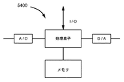
図61は、本発明の改善されたコンピュータシステムに採用される他の実施例の高レベル概略ブロック図である。図61は、いかに図60の総合ブロック5500が、メモリ及び適当なAD変換ブロック、DA変換ブロックと接続している処理素子として分類されるかを示す。追加のI/Oもまた示されている。
【0177】
本発明は、図示の実施例を参照して説明されたが、この説明を限定的に解釈することを意図しているのではない。図示の実施の種々の変形ばかりでなく、本発明の他の実施例は、本説明を参照するならば当技術の習熟者に実施可能でありかつ明白である。したがって、添付の特許請求の範囲は、本発明の真の範囲に属するあらゆるこのような変形及び実施例を包含すると考える。
【0178】
以上の説明に関して更に以下の項を開示する。
【0179】
(1) 計算システムであって、
主CPUマイクロプロセッサ、
前記主CPUマイクロプロセッサとは異なる命令集合を有するDSPマイクロプロセッサ、
前記主CPUマイクロプロセッサと前記DSPマイクロプロセッサとに結合された記憶装置、及び
主CPUが他に係わって占有されている時間間隔中DSPが前記CPUの動作を実行することによって前記システムの性能を高めるように配置された前記記憶装置内のファイルベースオペレーティングシステム
を含む計算システム。
【0180】
(2) 第1項記載の計算システムであって、前記DSPマイクロプロセッサと前記主CPUマイクロプロセッサとに結合されたビデオ集積回路を更に含み、前記記憶がディスクとDRAMを更に含み、前記DRAMが前記マイクロプロセッサと、前記主CPUマイクロプロセッサと、前記ビデオ集積回路とに対して統一メモリアーキテクチャ内で結合される、計算システム。
【0181】
(3) 第1項記載の計算システムであって、前記システムのアプリケーションを支持する少なくとも1つのアプリケーション装置を更に含み、前記アプリケーション装置が物理層のみに実質的に減少させられたハードウェアを更に含み、それであるから、前記DSPマイクロプロセッサが前記物理層によって媒介される信号を利用して前記アプリケーションの残りを仮想化しかつ遂行する、計算システム。
【0182】
(4) 第1項記載の計算システムであって、前記DSPマイクロプロセッサによる実行用に前記記憶装置内にカーネルソフトウェアを更に含む計算システム。
【0183】
(5) 第4項記載の計算システムであって、前記DSPマイクロプロセッサに結合されたI/Oポートを更に有し、前記カーネルソフトウェアが前記ファイルベースオペレーティングシステムと適切に調整するDSPマイクロプロセッサ動作を定義し、もし前記主CPUマイクロプロセッサが仮想ハードウェアを表す所与の機能を実行するのに占有されるならば、前記DSPマイクロプロセッサが前記機能を実行し、もし前記主CPUと前記DSPの両方が自由であるならば、前記ファイルベースオペレーティングシステムによって決定されるに従って前記主CPUマイクロプロセッサ又は前記DSPマイクロプロセッサのどちらかが前記機能を実行することができ、前記仮想ハードウェアが前記CPUと前記I/Oとに係わる移動度を有する、計算システム。
【0184】
(6) 第4項記載の計算システムにおいて、前記カーネルソフトウェアが前記ファイルベースオペレーティングシステムを用いて割り込みベースでDSPマイクロプロセッサ動作を定義し、所与の機能に対する優先権が実時間に計算され、かつ機能がダイナミックに実行され、かつ前記カーネルソフトウェアが前記ファイルベースオペレーティングシステムを供給し、それによって実時間優先権を計算することができる、計算システム。
【0185】
(7) 第1項記載の計算システムにおいて、前記ファイルベースオペレーティングシステムが前記DSPマイクロプロセッサ用プログラム空間について、かつ更に前記主CPUマイクロプロセッサと前記DSPマイクロプロセッサとの共用メモリモデルとしての読み出しデータ送り手空間と書込みデータ受け手空間とについて前記記憶装置に対するポインタアドレスを前記DSPマイクロプロセッサに供給するソフトウェアを含み、それによって前記配置が前記ファイルベースオペレーティングシステムを使用して前記DSPマイクロプロセッサを前記主CPUマイクロプロセッサに緊密に結合する、計算システム。
【0186】
(8) ソフトウェアアプリケーションの少なくとも部分を実行する能力のある第1項記載の計算システムであって、前記ファイルベースオペレーティングシステムが、仮想メモリ内の何処にソフトウェアの部分が開始しかつ終了するか告げるハンドルを定義する前記ソフトウェアを含み、前記システムが前記DSPマイクロプロセッサに主CPU機能を実行させる動作を定義するDSPカーネルを更に含み、前記主CPUマイクロプロセッサは何処に送り手ハンドルと受け手ハンドルがあるかを定義し、前記ファイルベースオペレーティングシステムは情報を受け手ハンドルによって定義された位置へ送る動作を定義し、前記DSPカーネルは何処で前記送り手ハンドルと前記受け手ハンドルとが前記DSPマイクロプロセッサに前記主CPUの代わりに機能を実行させるべきかに基づき動作を定義する、計算システム。
【0187】
(9) 第1項記載の計算システムにおいて、前記主CPUマイクロプロセッサが仮想アドレスを利用し、かつ前記ファイルベースオペレーティングシステムが前記仮想アドレスに相当する物理アドレスを提供する仮想メモリマネージャを含み、かつ前記計算システムがDSPマイクロプロセッサ機能用物理アドレスを利用する動作を定義するDSPカーネルを更に含む、計算システム。
【0188】
(10) 第1項記載の計算システムにおいて、前記ファイルベースオペレーティングシステムが、16ビットアプリケーション用にコールバック機能を通して、かつ32ビット用にセマフォーを通してアプリケーションと通信する仮想デバイスドライバ(VxD)を定義するソフトウェアを含む、計算システム。
【0189】
(11) 第1項記載の計算システムにおいて、前記ファイルベースオペレーティングシステムが前記DSPマイクロプロセッサと前記主CPUマイクロプロセッサとの間を通信するために使用される割り込みを仮想化する動作を定義する、計算システム。
【0190】
(12) 幅を有するデータ入力、前記データ入力と異なる幅のデータ出力、アドレス入力、アドレス出力、及びアドレスとデータ幅と第1バスクロック周波数とを有する第1バスと前記第1バスと異なるデータ幅の第2バスであってかつアドレスを有する前記第2バスとの間のインタフェースとして使用されるようなデバイスとを有する集積回路デバイスであって、
前記第1バスクロック周波数に同期するFIFOの動作用クロック入力を有する少なくとも2つの並列複数語FIFO、
制御入力を有するマルチプレクサ電子回路であって、前記FIFOを経由して前記データ入力と前記異なる幅のデータ出力との間のデータのバイトを多重化するように結合された前記マルチプレクサ電子回路、及び
前記アドレス入力と前記アドレス出力との間でアドレスを翻訳するアドレス翻訳回路であって、前記アドレス入力が前記マルチプレクサ電子回路の前記制御入力に結合された最下位ビットを有し、それであるからデータバイトが前記アドレス入力最下位ビットに従って異なって多重化される、前記アドレス翻訳回路
を含む集積回路デバイス。
【0191】
(13) 第12項記載の集積回路デバイスであって、命令集合を有しかつ前記集積回路デバイス上に集積されたプロセッサを更に含み、前記プロセッサが前記アドレス入力と前記アドレス出力とに結合された、集積回路デバイス。
【0192】
(14) 第13項記載の集積回路デバイスであって、バイト使用許可出力を有し、かつ前記バイト使用許可出力をセットしかつ前記FIFOからのデータを前記データ出力に結合するために前記プロセッサに更に応答性の集積回路デバイス。
【0193】
(15) 第13項記載の集積回路デバイスであって、DRAMメモリコントローラとPCIバスインタフェースとを含むノースブリッジ電子回路を更に有する集積回路デバイス。
【0194】
(16) 第13項記載の集積回路デバイスであって、カードバスコントローラ電子回路を更に有する集積回路デバイス。
【0195】
(17) 第13項記載の集積回路デバイスであって、汎用直列バス(USB)とIEEE1394−準拠直列バスとを含む群から選択される直列バスコントローラ電子回路を更に有する集積回路デバイス。
【0196】
(18) 第12項記載の集積回路デバイスであって、前記アドレス出力に結合された散乱−収集DMA電子回路を更に有する集積回路デバイス。
【0197】
(19) 第12項記載の集積回路デバイスであって、前記データ出力に結合されたマスタ回路とスレーブ回路との両方を含むバス制御ブロック更に含む集積回路デバイス。
【0198】
(20) 主CPUマイクロプロセッサ、
前記主CPUマイクロプロセッサに結合された第1バスであって、アドレス線と、データ幅と、第1バスクロック周波数とを有する前記第1バス、
前記主CPUマイクロプロセッサと異なる命令集合を有する第2マイクロプロセッサ、
前記第1バスと異なるデータ幅の第2バスであって、アドレス線を有しかつ前記第2マイクロプロセッサに結合された前記第2バス、及び
幅を有するデータ入力と、前記データ入力と異なる幅のデータ出力と、アドレス入力とアドレス出力とを有し、前記第1バスと第2バスとへのインタフェースとして結合された集積回路デバイスであって、
前記第1バスクロック周波数に同期するFIFOの動作用クロック入力を有する少なくとも2つの並列複数語FIFO、
制御入力を有するマルチプレクサ電子回路であって、前記FIFOを経由して前記データ入力と前記異なる幅のデータ出力との間のデータのバイトを多重化するように結合された前記マルチプレクサ電子回路、及び
前記アドレス入力と前記アドレス出力との間でアドレスを翻訳するアドレス翻訳回路であって、前記アドレス入力が前記マルチプレクサ電子回路の前記制御入力に結合された最下位ビットを有し、それであるからデータバイトが前記アドレス入力最下位ビットに従って異なって多重化される前記アドレス翻訳回路
を有する前記集積回路デバイス
を含み、
、前記第2マイクロプロセッサが前記第2バスを経由して前記アドレス入力と前記データ入力とに結合されている
計算システム。
【0199】
(21) 改善されたPCシステム(100)であって、主CPUマイクロプロセッサ(102)と、ファイルベースオペレーティングシステム(図19a)と、DSPマイクロプロセッサ(200)とを含み、主CPU(102)が他に係わって忙殺されている時間間隔中前記DSP(200)が前記主CPUの動作を実行するように配置され、それによって前記PCシステムの帯域幅の増大が達成される。このPCシステムは多重CPU及び(又は)多重DSPを含むこともできる。
【図面の簡単な説明】
【図1】本発明による改善されたコンピュータシステムの実施例の電気回路ブロック図。
【図2】図1の改善されたコンピュータシステムの部分の好適実施例の詳細な電気回路ブロック図(部分的に概略図、部分的にブロック図)。
【図3】図1の改善されたコンピュータシステムの部分の一好適実施例の更に詳細な電気回路図(部分的に概略図、部分的にブロック図)である。
【図4】図1の改善されたコンピュータシステムの部分の好適実施例の詳細な電気回路ブロック図(部分的に概略図、部分的にブロック図)であって、aはその含むチップ内の構成図、bは全体の接続図。
【図5】ホスト依存性である非対称多重処理のための本発明の改善されたコンピュータシステムの一実施例のブロック図。
【図6】本発明の改善されたコンピュータシステムに対してスーパスカラ拡張を使用する実施例の概略ブロック図であって、aはCPUモデルの図、bはメモリキャッシュ階層構造図。
【図7】本発明の改善されたコンピュータシステムに対する共用メモリモデルの実施例の概略線図。
【図8】本発明の改善されたコンピュータシステムに対するマルチメディア拡張モデルの実施例の概略線図。
【図9】本発明の改善されたコンピュータシステムに対するシステム/キャッシュ/仮想メモリモデルの実施例の概略線図。
【図10】本発明の改善されたコンピュータシステムに採用されることがあるMPEG再生フィルタグラフモデルの実施例の概略ブロック図。
【図11】本発明の改善されたコンピュータシステムに対する仮想I/Oハードウェア−PCIDMA及びマルチメディア実時間割り込みハンドラモデルの実施例の概略ブロック図。
【図12】本発明の改善されたコンピュータシステムに対するフレーム内の並列処理の概略ブロック図。
【図13】本発明の改善されたコンピュータシステムが採用することがあるMPEGエンコーダの簡単化ブロック図。
【図14】本発明の改善されたコンピュータシステムが採用することがあるMPEGデコーダ1400の簡単化ブロック図。
【図15】本発明のノートブックコンピュータに対するビデオ解決の実施例の簡単化ブロック図。
【図16】本発明のデスクトップコンピュータに対するビデオ解決の実施例の簡単化ブロック図。
【図17】本発明の改善されたコンピュータシステムに対するDSPアルゴリズム用アップリケーションパイプラインの簡単化ブロック図。
【図18】本発明による改善されたコンピュータシステムの他の実施例の電気回路ブロック図。
【図19】本発明の改善されたコンピュータシステム流れ図と電気回路図であって、aはシステム流れ図、bは図1の改善されたコンピュータシステムの好適実施例の更に詳細な電気回路図(部分的に概略図、部分的にブロック図)。
【図20】本発明の改善されたコンピュータシステムに対するメモリ分配及び物理ロッキングモデルの概略ブロック図。
【図21】本発明の改善されたコンピュータシステムに対する送り手及び受け手データDMA転送テーブルモデルの概観ブロック図。
【図22】本発明の改善されたコンピュータシステムに対する送り手データDMA転送テーブルモデルの内部構造の概略ブロック図。
【図23】図22の送り手DMA転送テーブルに対する領域リストの詳細を示すブロック図。
【図24】本発明の改善されたコンピュータシステムに対する受け手データDMA転送テーブルモデルの内部構造の概略ブロック図。
【図25】図20のプログラマ/データ空間の部分テーブルの更に詳細なブロック図。
【図26】本発明による改善されたコンピュータシステムの他の実施例の電気回路ブロック図。
【図27】本発明による改善されたコンピュータシステムの他の実施例の電気回路ブロック図。
【図28】本発明による改善されたコンピュータシステムの更に他の実施例の電気回路ブロック図。
【図29】本発明による改善されたコンピュータシステムのなお更に他の実施例の電気回路ブロック図。
【図30】本発明の改善されたコンピュータシステムに対する仮想メモリモデルの実施例の電気回路ブロック図。
【図31】本発明の改善されたコンピュータシステムに対する仮想メモリモデルの他の実施例の電気回路ブロック図。
【図32】本発明の改善されたコンピュータシステムに対する図31及び32の仮想メモリ内の種々の作用を示す概略ブロック図。
【図33】本発明の改善されたコンピュータシステムに対する図31及び32の仮想メモリ内のなおまた種々の作用を示す概略ブロック図。
【図34】本発明の改善されたコンピュータシステムに対する仮想メモリモデルの他の実施例の概略ブロック図。
【図35】本発明の改善されたコンピュータシステムに対する仮想メモリモデルの更に他の実施例の概略ブロック図。
【図36】本発明による改善されたコンピュータシステムの部分の実施例の電気回路ブロック図。
【図37】本発明による改善されたコンピュータシステムの部分の実施例の電気回路ブロック図。
【図38】本発明の改善されたコンピュータシステムの部分の実施例の概略ブロック図。
【図39】本発明の改善されたコンピュータシステムの部分の実施例の概略ブロック図。
【図40】本発明の改善されたコンピュータシステムの部分の実施例の概略ブロック図。
【図41】本発明の改善されたコンピュータシステムの部分の実施例の概略ブロック図。
【図42】本発明の改善されたコンピュータシステムの部分の実施例の概略ブロック図。
【図43】本発明の改善されたコンピュータシステムの部分の実施例の概略ブロック図。
【図44】本発明の改善されたコンピュータシステムの部分の実施例の概略ブロック図。
【図45】本発明の改善されたコンピュータシステムに対するMPE再生フィルタグラフモデルの実施例の概略ブロック図。
【図46】本発明による改善されたコンピュータシステムの他の実施例の電気回路ブロック図。
【図47】本発明の改善されたコンピュータシステムに使用されるソフトウェアアプリケーション及びそれらの関連アプリケーションのブロック図。
【図48】本発明の改善されたコンピュータシステムに使用される音声デコーダの簡単化ブロック図。
【図49】直接DSP構成要素及びいかにこの要素をドライバ及びエミュレーションブロックとインタフェースさせるかの概略ブロック図。
【図50】本発明の改善されたコンピュータシステムに対する仮想メモリモデルの他の実施例の概略ブロック図。
【図51】本発明の改善されたコンピュータシステムを実現するWindowsアプリケーションと基礎をなすPCハードウェアとの間のソフトウェアの種々の層を示す概略ブロック図。
【図52】本発明の改善されたコンピュータシステムに対する図50の種々のモデル内の種々の作用を示す概略ブロック図。
【図53】本発明の改善されたコンピュータシステムに対する図50の種々仮想モデル内の種々の作用を示す概略ブロック図。
【図54】本発明の改善されたコンピュータシステムに対する仮想モデルの他の実施例の概略ブロック図。
【図55】本発明の改善されたコンピュータシステムに対する仮想モデルの他の実施例の概略ブロック図。
【図56】本発明の改善されたコンピュータシステム上で使用可能なマルチメディアに対する仮想モデルの他の実施例の概略ブロック図。
【図57】本発明の改善されたコンピュータシステムを実現するWindowsアプリケーションとその基礎をなすPCハードウェアとの間のソフトウェアの種々の層を示す概略ブロック図。
【図58】本発明の技術に従いDSPを含むブロックを提供するように選択されたアプリケーション機能性が一括組み合わせられる種々の方法を示す概略ブロック図。
【図59】本発明の技術に従いDSPを含むブロックを提供するように選択されたアプリケーション機能性が一括組み合わせられる代替方法を示す概略ブロック図。
【図60】本発明の改善されたコンピュータシステムに採用される他の実施例の概略ブロック図。
【図61】本発明の改善されたコンピュータシステムに採用される他の実施例の高水レベル略ブロック図。
【符号の説明】
100 PCシステム
102 CPU
104 キャッシュ
106 主メモリバス
108 ホストブリッジ
112 主メモリ
116 PCIバス
120 P1394/USBブロック
124 I/Oブロック
128 ISAバス
200 DSPブロック
210 ハードウェアインタフェース電子回路
214 インタフェース電子回路、メモリ
218 DSPコア
222 DSPコア
304 PCIマスタ/スレーブインタフェース回路
305 ハードウェア層
306 PCI構成制御及び状態レジスタ電子回路
308 PCI I/O空間レジスタ電子回路
310 2重ポート読み出し書き込みFIFO電子回路
312 DSP I/O空間レジスタ電子回路
316 インタフェース/コーデックDMA制御回路
420 チップ
424 マスタ/スレーブインタフェース
428 DSP
432 カードバスコントローラ
460 チップ
488 データバッファ
APP アプリケーション
FFD フロッピィディスク装置
HDD ハードディスク装置
MUX マルチプレクサ
PCI 周辺デバイス相互接続
PP 並列ポート
PPU 周辺処理装置
SP 直列ポート
UMA 統一メモリアーキテクチャ
VxD ビデオドライバ
WAN 広域ネットワーク[0001]
BACKGROUND OF THE INVENTION
The present invention generally relates to improved personal computer (hereinafter referred to as PC) circuits, computer systems, and methods of operation thereof.
[0002]
[Problems to be solved by the invention]
Early computers took up a lot of space and occupied the whole room. From time to time, minicomputers and desktop computers have been on the market.
[0003]
Popular desktop computers include "Apple ™" (Motorola ™ 680x0 microprocessor-based) and "IBM ™ -compatible machine" (Intel ™ or other x86 microprocessor-based). These are known as PCs and have become very popular for office and home use. High-end desktop computers called workstations based on some superscalar and other very high performance microprocessors such as SuperSPARC ™ have also been introduced.
[0004]
Further developing, notebook size or palmtop computers are optionally battery powered for portable user applications. Such notebooks and small computers are challenging technologies that are faced with the incompatible goals of miniaturization, continually higher speed, higher performance, more flexibility and longer battery life. Also, a desktop enclosure called a docking station has a portable computer that fits into the docking station, and improvements to such portable computer / docking station systems are desired. However, in all these systems, the selection of a central processing unit (hereinafter referred to as CPU) generally determines the processing power of the system and an add-in card, ie, an embedded card is added to the CPU. Thus, it is CPU-centric in the sense of adding a specific application or function such as a modem or multimedia. Improvements in circuits, integrated circuit devices, all types of computer systems, and, among other things, ways to address the challenges listed above are desired as described herein.
[0005]
[Means for Solving the Problems]
Overall, and in one form of the invention, a PC system includes a main CPU microprocessor, a file-based operating system, and a digital signal processor (hereinafter referred to as DSP) microprocessor, which are the other main CPUs. The DSP is arranged to be able to perform main CPU operations during the time interval occupied, thereby increasing the bandwidth of this PC system. The PC system can also include multiple CPUs and / or multiple DSPs.
[0006]
In another form of the invention, a combined video / imaging system that includes a DSP microprocessor, video / audio control logic, and compression / decompression electronics, together comprises a DSP microprocessor, a main CPU microprocessor, and both A memory management circuit coupled to the processor, and a memory circuit coupled to the memory management path and a local bus, so that the memory circuit comprises a DSP, a main CPU, a video / audio control logic circuit, and a compression / Serves as a unified memory architecture for decompression electronics, and the DSP performs processing functions for both video / audio control logic and compression / decompression electronics. In addition, software that virtualizes parts of the video / imaging function may be added to the system.
[0007]
The present invention provides a system for comprehensively upgrading the software of a PC.
[0008]
The present invention provides a system that improves performance by collectively handling add-in features, ie, embedded features, through an add-in card.
[0009]
The present invention provides a methodology for integrating features in core logic for motherboard implementation.
[0010]
In the present invention, all functions of the system are integrated on a CPU chip.
[0011]
The present invention has at least one piece of main CPU, DSP, and application hardware reduced substantially only to the physical layer, so that the DSP is associated with the application associated with the signal mediated by this physical layer. Provide a system that virtualizes and fulfills the rest. This system may employ a large number of applications and layers. The DSP virtualizes, for example, a local area network (hereinafter referred to as LAN), video controller, image compression / decompression electronic circuit, fax machine, and modem.
[0012]
The present invention provides a DSP core, a master / slave bus interface, a memory circuit including a first-in first-out (hereinafter referred to as FIFO) function coupled to the interface, and an integrated circuit having a RAM function coupled to the DSP core.
[0013]
The present invention provides an integrated circuit including a DSP core, a master / slave bus interface, a memory circuit including a FIFO function coupled to the interface, and a single instruction / multiple data control circuit coupling the memory to the DSP core. To do.
[0014]
The present invention includes a DSP core, an interface circuit including a master / slave bus interface and a translation circuit, a memory circuit including a FIFO function coupled to the master / slave bus interface and a RAM function coupled to the translation circuit. Provides an integrated circuit coupled to the memory circuit and an interface.
[0015]
The present invention relates to a video controller including a bus mastering circuit having a first bus interface circuit, a display controller circuit having a display interface, and a second bus interface circuit, wherein the display controller circuit is coupled to the second bus interface circuit. An integrated circuit is provided.
[0016]
The present invention provides the following software system. That is, a software system having an operating system, at least one multimedia driver, an x86 object code application, a non-x86 DSP code application that virtualizes a hardware application, and DSP kernel software, the kernel software comprising: Or) in conjunction with multimedia real-time events, perform real-time interrupts and / or direct memory access (hereinafter referred to as DMA) virtualization and / or multi-thread multitasking operations within the DSP core. Memory transaction functions and / or inputs / outputs that are operable on the DSP core and / or otherwise performed by the x86 Hereinafter referred to as I / O) to perform a transaction function.
[0017]
The present invention includes a processing element, an interconnect circuit connected to the processing element, a memory electronic circuit connected to the processing element (or the interconnect circuit), a multiplexed bus connected to the interconnect circuit, A computing system having a virtualization circuit connected to the multiplexed bus to perform a selected application function is provided.
[0018]
The present invention includes a first multiplexed bus interface circuit, a second multiplexed bus interface circuit, and at least one signal processing element connected to the first multiplexed bus interface circuit and the second multiplexed bus interface circuit in advance. A virtualization circuit that performs a selected application function is provided.
[0019]
Other improved PC devices, systems, and methods of operation thereof are also claimed in the claims.
[0020]
The present invention will be understood by reference to the following detailed description in conjunction with the accompanying drawings.
[0021]
In these attached drawings, unless otherwise indicated, parts having the same function are denoted by the same reference numerals.
[0022]
DETAILED DESCRIPTION OF THE INVENTION
Referring initially to FIG. 27, a block diagram of the
[0023]
A
[0024]
The PCI bus 2710 is connected to the CPU in the
[0025]
Peripheral processing unit (hereinafter referred to as PPU) 2718 serves as a system bridge that connects PCI bus 2710 to ISA /
[0026]
In FIG. 27,
[0027]
In general, the other blocks connected to PCI bus 2710 in FIG. 27 cost about as much as all peripheral devices connected to ISA /
[0028]
Cost reduction loadmap, future sophistication, and compatibility with existing ("heritage") software goals are important goals for any improved PC system. The system embodiment of the present invention confirms and proves that improvements at the system level can achieve these goals. In particular, the system embodiment confirms that any of the PC motherboards preferably preferably occupy only a low cost, no software, and essentially negligible motherboard area.
[0029]
Backward compatibility with DOS and Windows ™ 3.11 may be provided by the “virtual” hardware of the present invention. Virtual hardware means that all the functions shown in FIG. 27 are fixed and dedicated and not updatable even if these functions are distributed. Software can help to virtualize them. If a chip implements all of the functions shown in FIG. 27, this chip will be very programmable. Accordingly, the various embodiments of the present invention are some programmable enough to “virtualize” all of the functions shown in FIG. 27 in combination with all the redundant and incompatible hardware shown in FIG. And ultimately provide a single chip that performs these functions.
[0030]
Windows is a recent and future PC operating system (hereinafter referred to as OS) and dynamically links to libraries so that software does not have to be compiled and linked before run time, for example Dynamic link loading (hereinafter referred to as DLL) is not linked until run time and provides virtual software. This reduces the software size.
[0031]
In general, conventional CPU systems use fixed CPU hardware to implement various applications, but the CPU cannot be involved in the AT bus or all the I / O ports shown in FIG. . In one embodiment of the invention described later in this specification, the hardware can do this positively.
[0032]
For multimedia applications, the
[0033]
The virtual hardware has mobility related to the CPU and the OS at the same time. Since no way is known to physically achieve this, virtualization is implemented in accordance with the teachings of the present invention. A DSP solution and core that are programmable serve as the basis for virtual hardware, which is customized and improved as described herein.
[0034]
The DSP core is a highly advantageous basis for running the various virtualizations necessary for embodiments of the present invention. However, DSP utilizes memory peripheral devices and a local DSP bus, which introduces additional challenges. Using the teachings of the present invention, diametrically different DSPs can be made to “look” like x86 CPUs, such as Pentium®, or vice versa.
[0035]
A software link is used to tightly couple the DSP and its peripheral devices to the x86 CPU, and to do this, use a popular OS such as, but not limited to, Windows 95. This software link couples the two tighter than if the DSP and its peripheral devices are on the same chip. Therefore, everything is made in software and the line between hardware and software is not clear, achieving some significant advantages. The end result is a single chip with software that can be advanced remotely by telephone line or by transfer of control information.
[0036]
FIG. 19a shows the dominant layered architecture within Windows 3.11.
[0037]
This provides a way to plug into the client / server architecture within the Windows architecture. Therefore, a DSP server or audio compression server can be plugged in through Windows, and their mechanisms are all the same. FIG. 19a shows how to plug in any desired architecture to Windows. This is also the key to backward compatibility and establishes a new and non-intrusive composition for the future.
[0038]
Next, in FIG. 19b, the virtual hardware environment 1922 is a TI TMS320C5x DSP with special DSP kernel software that is compatible with the largest third party installed software base (eg, modem, audio equipment, etc.) already available. However, it is realized without being limited to this. Everything runs on a preemptive basis, and priority is calculated in real time and executed dynamically. However, something must supply the OS so that the OS can calculate the priority in real time. Some of that is real-time kernel software 1922. This complements Windows OS and is not incompatible with it, and works to extend it. This provides a multithreaded and multitasking system.
[0039]
Next, the audio converter block 1926 performs audio compression / decompression on the DSP side, whereas the ACM driver block 1918 can perform the same function on the CPU side. However, if the CPU is occupied and does not have time to perform this mechanism, the DSP may handle it. If both the CPU and the DSP are free, either or both of these can perform this function due to the software's ability to not blur the line between the CPU and the DSP. Therefore, all as an advantageous result through the OS, the CPU can embody the DSP, and the DSP can embody the CPU. Conventionally, the CPU performs data movement because the CPU can perform movement in 32 or 64 bit chunks. However, in the present invention, an algorithmic intense block in an application call to the DSP does that. In this way, it can be said that the application is accelerated.
[0040]
The
[0041]
FIG. 1 shows a block diagram of an
[0042]
The
[0043]
In FIG. 1, past modems are virtualized by providing the DSP block 200 with appropriate modem software. Other similar applications that may be virtualized are speaker horns, speech, digital simulated voice and data modem (DSVD), T.D. 120 transport layer, VDSVD (video digital voice and voice). The “oval block” in FIG. 1 shows some of these applications.
[0044]
Other virtualizable applications include video compression / decompression vector quantization (hereinafter referred to as VQ), video compression / decompression MPEG, ISDN based indoor conference H.264. 320, HTN based on ATN and LAN. 321; There are video conferences over 322 and telephone lines.
[0045]
Still other virtualizable applications include 3D graphic display applications and 3D audio for transport directional audio.
[0046]
Many of these applications include professional audio, games, hard disk drives, printers, fax data modems, telephone answering machines (DTADs), multimedia CD devices, and data / file compression, the latter being system traffic and Performed by the DSP to reduce the CPU burden, there is also format conversion, and digital filter and digital conversion.
[0047]
FIG. 1 includes the P1394 /
[0048]
To borrow the cost from the cellular phone, the hardware is removed from the cellular phone design and transferred to the PC. Therefore, cellular telephones are no longer isolated systems.
[0049]
Therefore, for each home application, the hardware is removed from the application, as is currently known, and the hardware is moved to a virtualized PC.
[0050]
Similarly, the RF hardware of the I / O block 124 is virtualized so as to be only the physical layer. Therefore, the PC system is truly multifunctional and multitasking.
[0051]
FIG. 2 shows a more detailed block diagram of the virtual DSP block 200 of the
[0052]
In FIG. 2, the
[0053]
The heart of
[0054]
The
[0055]
Therefore, advantageously, the
[0056]
As different clocks run on different chips, the clocking challenge is solved in
[0057]
DMA transactions are preferably based on flow-I / O. The CPU operates in the virtual space, but the DMA works in the physical space. Translation is preferably performed by the DSP under software control using Windows 95, without resorting to old or new hardware in the
[0058]
[0059]
The Windows software architecture requires everything to look like a file transaction under Windows. File transactions are memory transactions, and it does not matter which CPU or DSP is performing them. The CPU can only do one thing at a time, so the DSP does the work during the system downtime and meets the downtime, so no hardware is needed. This ability to cherry pick and work during downtime is an important advantage of this research study that cannot be performed by the CPU. All these chips, such as video chips, DSPs, CPUs,..., Are governed by the same constraint that every transaction must be a memory transaction or a file transaction (or an I / O transaction that is less important for this purpose). . Everything is treated equally under the OS.
[0060]
3 is a more detailed electrical schematic (partially schematic, partly block diagram) of one preferred embodiment of the portion of the improved computer system of FIG. FIG. 3 schematically illustrates the
[0061]
4a is a more detailed electrical schematic (partially schematic, partly block diagram) of a preferred embodiment of the portion of the improved computer system of FIG. In FIG. 4 a, the
[0062]
[0063]
Since typical or conventional memory cycles are too long, the memory must also change. Memory cannot be a product in terms of functionality. So the memory needs additional functionality and this must be interfaced to the new block. The present invention takes advantage of the memory with this additional functionality.
[0064]
In FIG. 4b, the
[0065]
The
[0066]
From UMA block 492, one embodiment has an uncompressed output of up to 11 Gbytes / s on
[0067]
The
[0068]
FIG. 5 shows a block diagram of one embodiment of the improved computer system of the present invention for host-dependent asymmetric multiple processing. In FIG. 5, the P5 processor is a CPU. In FIG. 5, any CPU / IDSP intelligence in the PC can be centralized through the virtual technology of the present invention in the amount necessary to support the application, and then dissolve after the application is stopped. can do. A user need only have a given amount of computational resources required for a given application at any given time.
[0069]
A number of IDSPs that meet the needs of any particular application are shown in FIG. These chips are designed differently to properly interface to the ISA bus and the PCI bus. Some examples are shown in FIG. Although IDSP blocks are shown attached to these buses, they may be attached to either a north bridge or a south bridge, and may be integrated within the function of the block. Good.
[0070]
FIG. 6a shows a schematic block diagram of an embodiment of a CPU model that uses a superscalar extension for the improved computer system of the present invention. In FIG. 6b, the new chip has three pipelines, which are two conventional superscalar pipelines and a third DSP operations pipeline. That is, the superscalar CISC / RISC and DSP CPU architecture has three operations dispatched on a single chip. There is microcode storage in the CISC. The DSP core is a DSP hardware microstore, which dispatches DSP operations. The DSP core is "empty" until the user clicks on the Windows icon and then the DSP code is cached from hard disk to main memory, local memory for execution. In this way, the x86 CPU does not have to perform non-standard operations and dispatch DSP operations. Such a combined architecture is compatible with Windows 95.
[0071]
FIG. 6b shows one such memory cache hierarchy.
[0072]
This is a software cache including a
[0073]
As an example, a single V.P. The 34 modem uses 64K of code and data spacing as before because the modem speed negotiation requires this modem to talk to any other modem. During the 75 ms period, this modem knows what other modems are talking about, and then switches on for only a piece of code to maintain the specific application corresponding to that modem as a result of the negotiation. Put in. In this way, less code and data are required compared to the prior art.
[0074]
Having a transfer rate of 132 Mbyte / s allows many applications to easily move the required code from memory to the DSP local memory that executes it.
[0075]
FIG. 7 shows how a shared memory model is used to couple the DSP and CPU. Shared memory modems based on the Windows architecture tightly couple the DSP and CPU asymmetrically over any underlying symmetric software architecture.
[0076]
In FIG. 7, Windows has an architecture that calls a file drawer-like handle that tells where in the virtual memory the software starts and ends. These handles provide a mechanism for indicating the location of memory resources in the virtual memory space. With these handles, the DSP can be performed by the host CPU. The host tells the application that it needs to manipulate certain memory contents and where the source handle is and where the destination handle is. Content-based Windows sends information to the location defined by the receiver handle. 1) Knowing where the sender handle is, and 2) Knowing where the receiver handle is, the DSP enters operation and handles the transfer on behalf of the CPU. According to the application, the virtual memory manager of the OS tells the CPU where the physical address is. The CPU also has on-chip hardware that assists in determining the physical address. The DSP queries the OS's virtual memory manager as a superbus master (eg, this master can cross the page boundary unlike a simple bus master). Unlike a CPU that handles handles as virtual addresses, the DSP locks the handles to make them actual physical addresses while the application is running. The DSP lock is a utility written in the main DSP driver in the HAL layer, and activates an existing utility in the OS virtual memory manager to restore the physical address.
[0077]
FIG. 8 is a schematic diagram of an embodiment of a multimedia extension model for the improved computer system of the present invention. In particular, it can be seen that the real-time service provided by the IDSP of the present invention also provides real-time priority to the Windows OS interrupt scheduler, which is multi-threaded and multi-tasking. Figures 32 and 33, which will be discussed later, show details of how to handle interrupts to provide real-time capability. FIG. 35 shows the details of a certain real-time service.
[0078]
FIG. 9 is a schematic diagram of an embodiment of the system / cache / virtual memory model for the improved computer system of the present invention. The DSP core is a cache that moves data and instructions back and forth very efficiently. The CPU moves data from the hard disk to this cache. The improved cache operation method for PC of the present invention will be described.
[0079]
In FIG. 9, the code is extracted from the hard disk device (also referred to as HDD) to the
[0080]
FIG. 10 is a schematic block diagram of an embodiment of an MPEG playback filter graph model that may be employed in the improved computer system of the present invention. When the user clicks on a software object in FIG. 10, Windows dynamically allocates memory and runs object linking embedding (hereinafter referred to as OLE). MPEG works from objects to objects instead of layers to layers. The sender may include image capture data for decompression.
[0081]
FIG. 11 is a schematic block diagram of an embodiment of a virtual I / O hardware-PCIDMA and multimedia real-time interrupt handler model for the improved computer system of the present invention. In FIG. 11, the system intercepts the interrupt in real time. The DSP space is an external static RAM (hereinafter referred to as SRAM) that is resident in the
[0082]
FIG. 12 is a schematic block diagram of parallel processing by CPU and IDSP in a frame for the improved computer system of the present invention. In FIG. 12, given a frame, the host CPU must perform all processing and monopolize a number of slots in the
[0083]
Therefore, a relatively medium performance DSP has enough resources to do the main image processing because it is dedicated to its signal processing task. LANs, modems, and other applications are time shared with image processing, but during other time intervals unrelated to the analysis point of FIG.
[0084]
FIG. 13 is a simplified block diagram of an
[0085]
FIG. 14 is a simplified block diagram of an
[0086]
FIG. 15 is a simplified block diagram of an embodiment of video resolution for a notebook computer of the present invention that may employ a P5 processor as the CPU. In FIG. 15, the system works using the PCMCIA standard, revision 2.1, as shown in FIG. 4a.
[0087]
ZV does not require an extra frame buffer and is compatible with video input resources accommodated in the frame buffer. PCI is not isochronous, but is bursting and interrupted, and is therefore very disadvantageous for video. According to the present invention, isochronous capability is provided by a dedicated backdoor private high speed bus ZV connected to the frame buffer. It is the acceleration bus that links the blocks together in the
[0088]
FIG. 16 is a simplified block diagram of an embodiment of video resolution for a desktop computer of the present invention that may employ a P5 processor as the CPU. FIG. 16 shows a desktop PC that does not use PCMCIA or a card bus. Therefore, during playback of MPEG video, the CPU performs the video decoding function while the DSP performs the audio decoding function or vice versa. If data comes from a CD ROM, system synchronization is performed by the CPU. If data comes from an
[0089]
FIG. 17 is a simplified block diagram of an application pipeline for the improved computer system of the present invention. In FIG. 17, a single processor cannot be pipelined at the application level, even if it is a superscalar processor. This is clearly different from the pipeline pipeline hardware pipeline. What is meant is that different parts of the pipeline are executed at the same time to pipeline the application.
[0090]
The stage is established by the nature of the application. For example, while the DSP decompresses N frames of video, the x86 CPU simultaneously outputs processor data for frame N-1 to the screen and then repeats this cycle in a pipeline related manner. The DSP also performs filtering, scaling, and color conversion, while the CPU inputs data or outputs data.
[0091]
FIG. 18 is a block diagram illustrating the system level of another embodiment of a hardware architecture for an improved computer system in accordance with the present invention. FIG. 18 shows an alternative arrangement of the simplified block diagram of FIG. FIG. 18 shows a PDC that uses a PCI bus and has a slot 1810 for a plug-in PCI card 1820. The plug-in PCI card 1820 includes a PCI interface (I / F) 1822, a
[0092]
The PCI card 1820 is both a PCI master and a PCI slave. The host CPU can access the PCI configuration register and main memory pointer register in slave mode. In master mode, the DSP can use scatter-collect DMA to retrieve program code and data and store it in main memory.
[0093]
FIG. 19b is a more detailed electrical schematic (partially schematic, partly block diagram) of the preferred embodiment of the improved computer system of FIG. FIG. 19b is similar to FIG. 3, but further shows details of the DSP 1950 and associated
[0094]
The DSP 1950 runs independently of the CPU. When the PCI card is a slave, the CPU downloads an initialization code to the DSP after reset, where the DSP is independent. The CPU can start the DSP by setting the START bit in the PCI I /
[0095]
The CPU supplies a pointer address to the main memory. The three required addresses are the base address for the DSP's 128K bytes for the program space, the address for the 128K bytes for the read space (sender), and the address for the 128K bytes for the write space (receiver). Depending on the application, they point to different areas of memory, or the same area of memory. The CPU controls the DSP by writing to a
[0096]
The other bit in
[0097]
The PCI application card DSP architecture is initially memoryless. This is of interest to system manufacturers who need to keep costs as low as possible. However, this architecture does not preclude the addition of external program space memory or external data space memory, as indicated by
[0098]
In the absence of external memory, the only way to make code into the DSP executable is to reset the DSP and load a small initialization program from main memory using a ROM-based boot loader. That is. The DSP bootloader version ("BDSP") is used in the following description. The DSP reads the reset global memory address FFFF to determine what type of bootloading will occur. A value of 1100 in the four least significant bits indicates a 16-bit parallel I / O load using an XF signal for handshaking and a basic I / O (hereinafter referred to as BIO) signal. When BIO is low, the data bus is driven. After the boot load is complete, the BIO must remain high to prevent bus collisions on the DSP data bus.
[0099]
By loading 16-bit words via the I / O boot mode, the CPU can quickly load the basic main memory initialization program into the DSP. The DSP goes into a reset state, so the DSP can only respond to PCI bus transactions as a slave. The PCI host will control the initialization program values loaded into the DSP. This allows the initialization program to be modified by software. After this routine is loaded, the DSP is released from reset, so the DSP can execute the initialization program (also set the BIO select bit to allow the DSP's BIO signal to be driven with the FIFO status signal). Must be set). The initialization program acts as a PCI bus master and enters main memory to actually retrieve the DSP application software. By bootloading only the initialization program, the DSP PCI bus master can actually control the loading of the DSP application code.
[0100]
If the DSP application software cannot fit entirely in the DSP internal memory, more code needs to be swapped in. This code is retrieved from main memory. In order to retrieve a lot of code, a DSP application may perform a BLDP (Block Load Program to Data) instruction, which retrieves global space data and moves it to program space. If the global data space is designated as external memory and the program space is designated as internal memory, the BDSP performs the external access necessary to move the code. Since the DSP is taking out the global data space to the outside world, its application software needs a mechanism that tells the PCI interface that the DSP code is being taken out on the bus and is not data. The I / O port register bits will be used to indicate whether it is the program space code, the sender data, the receiver data, or the DSP determined data that is being retrieved. The I / O port register bit is set to access the program space that has been reset.
[0101]
The first bootloaded code that was brought into and used in the application code is preferably maintained in memory. This causes the CPU to abort the DSP operation by forcing an interrupt to reload this application. If this code is lost, the CPU has no control over the DSP and must reset the DSP to reload the program code. The DSP application software can transfer data from the external memory to the internal memory and restore it by a BLDD (Block Load Data to Data) command.
[0102]
The PCI interface is both a PCI master and a PCI slave. This interface needs to be a slave so that the CPU can access the configuration space. The CPU can access either the memory space or the I / O space to perform certain controls on the DSP and assemble the main memory pointer. The DSP will be a PCI master to access main memory for code and data. There is also a
[0103]
Configuration registers required by the PCI standard are used to specify areas in the PCI I / O space and memory address space with 0 and 1. The required PCI space is 5 double words. Since the address space should be 2 and required, 8 addresses must be reserved. The registers above these five doubles that are needed are not used and will return 0 if read. These five double words are used for the program space pointer, data space pointer, DSP command, DSP status word, and I / O port for bootloading the BDSP.
[0104]
The PCI host writes the PCI I /
[0105]
When the DSP algorithm is finished, the EVENT INTERRUPT bit in the status word is set. When this bit is set, an interrupt is generated to the application software through the PCI bus. Since this interrupt is controlled by the DSP software, interrupt enable is not implemented in hardware.
[0106]
The DSP hardware control word directly controls the operation of the DSP hardware. The least significant 4 bits are a retry counter bit. The retry counter bit causes this function to retry it if the PCI macro function initially fails the PCI transaction. This value is reset to 0000 which will cause the listed function to retry indefinitely. This value can be varied to be between 1 and 15 retries. If the retry counter will not run because no transaction is performed, the Retry Counter Expired bit in the MISC CTRL register is set. This state is available to the host.
[0107]
The DSP interface ASIC includes a PCI interface, a PCI FIFO, a DSP (connected device) interface, and a CODEC interface. This research requires that the BDSP is a discrete chip.
[0108]
The DSP has 5 user interrupts available. One of these interrupts is not maskable and four are maskable. The CODEC interface requires 3 interrupts, and the PCI interface register requires 2 interrupts and the RESET pin. These interrupts are used as follows. NMI-Master abort (from PCI host to DSP), INT1-CDRQ (from codec), INT2-PDQR (from codec), INT3-IRQ / IRQ2 (from
[0109]
The DSP accesses the memory mapped I / O port, which is used to control the operation mastering PCI macro.
[0110]
The CODEC register is used by the DSP to communicate with the discrete CODERC on the PCI application board. The FIFO state is available by the DSP at the I / O port. Depending on this ASIC or future revision of the ASIC, the FIFO may have different dimensions. Knowing what size FIFO the DSP must work with in order to tune the performance will aid the DSP. The FIFO size register displays the maximum number of words that the FIFO can hold. The number of DSP words to be transferred is written to another I / O port. This value is doubled in hardware to get the number of bytes to transfer. The maximum number of words that can be transferred is 32768 (65536 bytes). This means that the most significant bit of register 0x59 cannot be used. If a 1 is written to that bit, it is ignored.
[0111]
The PCI address offset (0x58) is an address in the DSP space that is transferred into the PCI space and used to transfer data to or from the host. The DSP accesses the host main memory by writing the DSP pointer to the PCI adder (Adder) pointer register, which takes up 2 DSP words and creates a 32-bit PCI pointer. This is useful if the DSP needs to calculate the location in main memory that has a database in the scatter-collection table. The PCI address space select bit in the PCI control register determines whether to use the DSP pointer or PCI pointer written to the PCI / O space when a PCI bus transaction is initiated.
[0112]
The codec status / mode register (0x5F) can be read for all 16 bits. Only the lower 8 bits are writable (the upper 8 bits are only read), and the BIO selection allows a flexible selection of the FIFO state or user signal connected to the DSP BIO input. All of the status signals, and therefore BIO, are high and active.
[0113]
The DSP performs reads and writes to and from the PCI bus through a 64-byte FIFO on the PCI ASIC. The PCI FIFO is configured as a 2-parallel 16-word FIFO that is synchronized with the PCI clock. The DSP control signal is synchronized with the CLKOUT1 signal of the DSP. Two options are available for clocking the processor. The first option divides the PCI clock by 2 and uses the DSP's CLKIN2 input to internally run the DSP at the PCI clock rate (up to 33 MHz) (which doubles the CLKIN2 signal by 2). become). This results in a situation where the PCICLK signal has the same frequency as the CLKOUT1 signal. However, the CLKOUT1 signal may be phase shifted up to about 270 degrees. Delay through the clock divider electronics and phase shift through the DSP phase-locked loop (hereinafter PLL) may cause a total delay of up to 25 ns. The second option is to divide the PCICLK signal by 1 and use the divide input option by 1 in the DSP (DSP does not support this mode). The net result will be that the PCICLK signal is still at the same frequency as the CLKOUT1 signal, but its phase is different.
[0114]
The DSP's RDz (Read Enable--Low Active) and WEz (Write Enable--Low Active) signals are used to generate FIFO read and write pulses. The DSP read must be performed in at least 3 software wait states to ensure that clock delay is taken into account.
[0115]
In order to ensure that the clock delay is taken into account, writing by the DSP must be performed with at least two software wait states.
[0116]
The DSP manages the data coming from and going to the FIFO. This data stream cannot be transparent to the DSP unless it overruns and underruns [the DSP may outrun the PCI bus and overrun the FIFO]. In order for the DSP to make best use of resources, the BIO signal is to be used as a flag to tell the DSP when it has data to read or when the FIFO is empty during writing. There are two methods for performing writing from the DSP. The first method is to wait until the FIFO is empty (before reading or writing), and then read or write a number of words that satisfy the FIFO. This will handle 32 words in the current hardware configuration and guarantees that the FIFO will not be overrun or underrun. After reading or writing 32 words, the DSP can put a BIO signal in the loop (this indicates that the FIFO is ready to receive the other 12 words) and can read or write the other 32 words. .
[0117]
The second method is to transfer a block of data larger than 12 words. This method uses the BIO signal, but the DSP puts the BIO signal in a loop before every read or write to the FIFO. Half empty and half full flags can be used to indicate the FIFO status via the BIO signal for these operations. The DSP uses its I / O space to set a bit in the control register to initiate a PCI transaction. The control register parameters are a PCI address space selection bit, a FIFO reset bit, a PCI macro bit, a DSP status bit, a start bit, and a BIO selection bit. A status register is also needed to check the status of the FIFO before the transaction begins. The parameters required to initiate a PCI bus transaction are the DSP address (which is translated into a PCI main memory address), the number of words to transfer (the hardware converts the number of words to a number of bytes), and Direction.
[0118]
When only two words are transferred over the PCI bus, signal data phase transfer occurs. These two words only satisfy one 32-bit transaction. The PCI macro needs to know this special situation in order to properly handle the PCI protocol. The value (number of words) written by the DSP is doubled to get the number of bytes, so the minimum number of bytes is 2. There are actually 4 bytes to transfer. If less than 4 bytes are transferred, the DSP must change the PCI bus byte grant bit or two of the 4 bytes of the PCI data phase will not be valid. The direction bit is important because this is a determinant in the input sender of the FIFO. The direction bit is automatically set when the DSP writes to the FIFO (this prevents setting the bit, writing the FIFO, and then starting a transaction). When reading from the PCI bus, the direction bit is set by writing to the register that initiates the transaction. The BIO signal is selected according to the value of the BIO selection register. This value must be changed each time there is a change between the read operation and the write operation.
[0119]
After these parameters are written to the interface ASIC, the PCI transfer is started when the start bit is written by the DSP. An example of the DSP order is as follows. That is,
[0120]
DSP reading order
1. Write the address of the transferred data.
2. Write the number of words to transfer (≧ 2).
3. Write end (DONE) bit (clear it), working bit (set it), transfer direction (0 = read), BIO select, and start (START) bit.
[0121]
Once the start bit is set, the hardware is:
3.1 Wait for the PCI bus to become free (P2CDGNTCUPL signal goes inactive).
3.2 Write to the register to set the CD2PREQCULPL and CD2PGNTCUPL signals.
3.3 Wait for the P2CDGNTCUPL signal to go active.
3.4 Write to register to set CD2PMSTCUPL signal (to prevent other transactions).
3.5 Strobe the new address, number of bytes, direction, and polyphase state to the macro.
3.6 Start the operation to fill the FIFO.
4). Wait for the macro to display that the FIFO is not empty. (Bring this state to the DSP as BIO).
5. Read from FIFO. Reading can be done from the FIFO with a 2 cycle / 1 wait state instruction. These standby states are software standby states. The FIFO read pulse is generated by a DSP read signal. If the FIFO has no data, the BIO is not set and the operation is deferred (for which an internal timeout may have to be used). By using the BIO signal, the DSP waits for data. 3. Loop back to repeat until you are finished. When the PCI interrupt generation is complete, the DONE bit can be optionally set.
[0122]
If the PCI bus slave can run without waiting during the last two data phases, the PCI macro will fill the FIFO. If there is no wait state in the last data phase, the FIFO will not write the last word. The FIFO will have a FIFO Full-1 double word inside.
[0123]
DSP write order
1. Wait for the macro to display that the FIFO is empty. (This state is held in the DSP as BIO.)
2. Write to the FIFO. Writing can be done to the FIFO with a 3 cycle / 1 wait state instruction. These standby states are software standby states. The FIFO write pulse is generated by a DSP write signal.
3. Write the address of the data to be transferred.
4). Write the number of words to transfer (in this case 32).
5. Write DONE bit (reset it), working bit (set it), BIO select, and start bit.
[0124]
Once the start bit is set, the hardware is:
5.1 Wait for the PCI bus to become free (P2CDGNTCUPL signal goes inactive).
5.2 Write to register to set CD2PREQCUPL and CD2PGNTCUPL signals.
5.3 Wait for the P2CDGNTCUPL signal to go active.
5.4 Write to register to set CD2PMSTCUPL signal (to prevent other transactions).
5.5 Strobe the new address, number of bytes, direction, and polyphase state to the macro.
5.6 Warn the DSP that the FIFO is empty (use the BIO signal). 3. Loop back to repeat until completion.
[0125]
When the DSP accesses main memory, the DSP's 16-bit word oriented address must be translated into a 32-bit byte oriented address. This translation part requires that the 16 bits of the DSP be shifted one bit to the left (multiply by 2). This means that instead of addressing 64K words of memory space, the DSP can actually access 128K bytes of PCI host main memory. The PCI specification requires that PCI initiators wishing to use linear addressing (addresses increase linearly during burst transfers) leave the two least significant bits of the address as 00. This places a constraint on the DSP software that all fetches from main memory must start with an odd address (the least significant bit is 0). In order to provide flexibility for applications in main memory, the DSP data space and instruction space can be relocated on 4K boundaries.
[0126]
The PCI bus is a selectable width bus. Any 4-byte grant signal can indicate with activity that any or all of the 4 bytes on this bus are valid data. Assume that the DSP has a 16-bit bus, which has 16 bits of valid data on every transfer. While the DSP is an initiator on the PCI bus, all byte grant signals are active (all data is 32 bits). To transfer between the PCI bus and DSP bus, there are two 16 bits in parallel to capture PCI data. The DSP multiplexes the output of several FIFOs to obtain a 16-bit word. Multiplexing is controlled by the least significant bit of the DSP. A 0 on
[0127]
The stereo audio codec 1956 is an 8-bit device having an ISA bus interface. This codec is connected to a data bus that is separate from the DSP data bus. The DSP accesses this codec via the I / O space register. In order to prevent the DSP from being tied up waiting for the low speed ISA interface, the
[0128]
This state machine that governs the codec is controlled through a CODEC Status / Mode register in the DSP I / O address space. The state machine starts when 1 is written to the start bit. Depending on whether a read or write is required and whether a PIO access or DMA access is required, the state machine will either write the bytes to the I / O space register or codec contents according to the appropriate protocol. Or read them into their registers. The BYTE XFER COUNT bit determines how many bytes are transferred during a DMA operation (
[0129]
PCI card users have the option to include external memory in the DSP program space and data space. This memory (socketed for easy installation and removal) allows the DSP algorithm to maintain its current form until it can rewrite code taking advantage of access to host main memory Will be able to. Data space can be used to keep local data separate from the host main memory. Global memory is specified as an interface to the host system. This interface goes through a FIFO residing in the global memory space. This memory is accessed using a software standby state instead of the READY signal.
[0130]
The bootload process uses the global memory location 0xFFFF and the memory map I / O port 50h. This location is available in global memory if the BIO bit (DSP command word—bit 3) in the PCI I / O space register is set high. If BIO is set low, a read from location 0xFFFF will result in a bus collision between bootload data and global memory data. If the user must use global memory, the BR # signal from the DSP to the ASIC is gated with the user address decode signal, and the ASIC FIFO is activated when the user accesses the global memory. To prevent.
[0131]
PC BIOS system (hereinafter referred to as BIOS) software executed at power-on is responsible for discovering what kind of PCI card is installed in the system. This software is the so-called power-on self-test (POST) code and is responsible for performing generic initialization of the PCI application. After completing the initialization, the card is inserted into the main memory and its own program code is taken out.
[0132]
Once the PC is powered up, the DSP is held in reset until the host DSP driver releases the DSP reset. At this point, the driver writes to the PCI I / O space command word (COMMAND WORD) register to release the DSP reset. Therefore, the CPU bootloads the BDSP. This device driver downloads a 16-bit word to the DSP via the PCI I / O Space Bootload Data (BOOTLOAD DATA) register by looking for the BDSP to set XF, then valid data is bootload data. After writing to the register, set BIO (in the command word register). This does not require additional hardware in the PCI ASIC or on the application card. This causes some overhead for the host DSP driver. This is also the most flexible research study because the bootload code can be changed in the software. Once the DSP is initialized, the DSP waits for the CPU to write to the register and set the COMMAND bit. The COMMAND bit generates an interrupt to the DSP and causes the DSP to begin execution. One of the first things to do with this initial DSP code is to check for the presence of data memory. If a data memory is found, it must be determined whether the memory is 8 or 16 bits wide. The presence of the DSP global memory gives the DSP application the opportunity to store up to 64K words (or bytes) of data in high speed memory on the PCI card without having to go through the PCI bus to access the PCI card. means.
[0133]
FIG. 20 is a schematic block diagram of a memory distribution and locking model for the improved computer system of the present invention. The memory allocation and locking shown in FIG. 20 correspond to those shown in FIG. It is known through DSP software that there is a pointer to the DSP space. For each transaction, it is also known where the sender and receiver tables are. FIG. 20 provides a directory for the memory architecture. FIG. 11 represents a single sender space and a continuous receiver space. In Windows 95, this can be said for virtual space, but physical addresses are scattered over the entire space. Therefore, there is the term scattering-collection bus mastering by DSP.
[0134]
FIG. 21 is an overview block diagram of the sender and receiver data DMA transfer table model for the improved computer system of the present invention. In FIG. 21, each
[0135]
FIG. 22 is a schematic block diagram of the internal structure of the sender data DMA transfer table model for the improved computer system of the present invention. FIG. 22 shows a more detailed structure of the sender DMA transfer table compared to FIG.
[0136]
FIG. 23 shows details of the area list for the sender DMA transfer table of FIG. FIG. 24 is a schematic block diagram of the internal structure of the receiver data DMA transfer table model for the improved computer system of the present invention. FIG. 25 is a more detailed block diagram of the programmer / data space partial table of FIG. FIG. 24 shows details of the receiver transfer table structure. FIG. 25 shows details of the programmer / data space block of FIG. FIG. 23 shows details of the list area in any one of FIGS. These figures illustrate how the DSP and host CPU effectively share and coexist when using the same memory space, such as
[0137]
FIG. 26 is an electrical circuit block diagram of another embodiment of the improved computer system according to the present invention. In this embodiment, the memory management logic, memory controller, memory, and cache are combined into one block and connected to the CPU via a local bus. The local bus is then connected to a PCI bridge, which is connected to the PCI bus. In addition, a video /
[0138]
FIG. 28 is an electrical circuit block diagram of another embodiment of the improved computer system according to the present invention. In this embodiment, the CPU has a memory controller and PCI bridge integrated on its chip and is therefore directly connected to the memory and PCI bus. An integrated multimedia graphics controller is connected to the PCI bus and display. In addition, two optional chips are provided and connected to the PCI bus. One chip is for peripheral I / O COMBO with DSP. The other chip is for a PCMCIA controller with a DSP. The PC BIOS is connected to the I / O block so that the keyboard, mouse, and parallel port (hereinafter referred to as PP) are connected. In addition to a hard disk device (hereinafter referred to as HDD) and a floppy disk device (hereinafter referred to as FDD), a serial port (hereinafter referred to as SP) is connected to the DSP portion.
[0139]
FIG. 29 is an electrical circuit block diagram of another embodiment of the improved computer system according to the present invention. FIG. 29 is similar to FIG. 28, but the wireless LAN of FIG. 29 is integrated with the PCMCIA controller block and enhanced to include a 1394 data stream.
[0140]
FIG. 29 shows an embodiment in which all functions are provided with one chip and I / O is provided with a bare bond physical layer. Everything except the physical layer is the PC part. This embodiment avoids multiple peripheral electronics and can focus on the physical layer that requires Federal Communications Commission (FCC) approval. A line protection device (hereinafter referred to as DAA) is software, and has a capability of performing voice annotation with a speech codec. The LAN focuses on the physical layer, and the DSP virtualizes other LAN functions. In the ultimate digital innovation for cost reduction, everything but the physical layer is virtualized and the
[0141]
FIG. 30 is an electrical circuit block diagram of an embodiment of an application / driver model for the improved computer system of the present invention. The VxD environment (hereinafter referred to as VXDE) provides DSP-related low-level services for Windows applications, such as multimedia applications. The Windows 3.1 model of the DSP driver shown in FIG. 30 includes Windows VxD and Windows DLL. The DLL interface with or to the Windows application performs application callbacks and file I / O, handles interrupts, and interfaces with VxD. VxD is only responsible for locking down and freeing physical memory that may be used by the DSP.
[0142]
Under Windows 95, the above model is no longer appropriate because the Windows driver with which the DSP driver DLL needs to communicate is 16 or 32 bits. In order for both the 16-bit Windows driver and the 32-bit Windows driver to communicate with the DSP driver, the above model is modified as shown in FIG.
[0143]
FIG. 31 is an electrical circuit block diagram of another embodiment of an application / driver model for the improved computer system of the present invention. The model shown in FIG. 31 has Windows VxD, 16-bit Windows DLL, and 32-bit Windows DLL. These DLLs are only needed for communication between the Windows driver and the DSP VxD. However, for this model, DSP VxD is particularly responsible: it is interfaced with DSP, handles application callbacks, file I / O, etc., performs interrupts, and is given the name DSP VxD environment. ing.
[0144]
VXDE provides DSP-related low-level services for Windows applications, such as multimedia applications. For multimedia applications, these services include the following: NodeAdvise, NodeAllocate, NodeDestroy, NodeGetAttr, NodeGetData, NodeGetPosition, NodePause, NodePuttData, NodeResetStream, NodeRun, NodeSetAttr, NodeSignalEvent, NodeCovertData, NodeWaitSemaphore, NodeCreatSemaphore, and NodeDestroySemaphore.
[0145]
Windows multimedia applications communicate with VXDE through a 16-bit DLL or 32-bit DLL, and VXDE communicates with a Windows application through a callback function for 16 bits or through an event signaling mechanism [Semaphore] for 32 bits. connect. The VXDE communicates with the DSP by writing to the DSP's memory mapped port, and the DSP communicates with the VXDE by generating a hardware interrupt. However, this hardware is virtualized through VPICD by VXDE.
[0146]
For any Windows application that wants to communicate with VXDE, all it needs to do is use the API collection listed above along with a 16-bit DLL or 32-bit DLL (referred to as DSAPI.DLL or DSPAP32.DLL) That is. Preferably, the 16-bit DLL puts parameters in the call structure, marks the structure as a call from the 16-bit side, and then calls VXDE through the entry point. The entry point is located using the Int 2F function 1684h. On the other hand, the 32-bit DLL invokes VXDE through the DEVICEIOCONTROL interface. On the VXDE side, when a call is received from the entry point, the call structure pointer is translated into a linear address and the call is dispatched to the corresponding function. This function translates any type of pointer from a SELECTOR / OFFSET address to a linear address and then processes the call. If a call is received from the DEVICEIOCONTROL interface, the call is dispatched directly to the corresponding function without any translation.
[0147]
A 12-bit Windows application that wants to be notified when the DSP hardware has finished a particular task can do so by: putting a valid event handle in the OVERLAPPED structure and sending a pointer to VXDE. This therefore requires a call to WaitForSimpleObject on the event. For applications that do not want notification, assume that the parameter containing the pointer to the OVERLAPPED structure is zero when calling VXDE.
[0148]
A 16-bit Windows application that wants to know when the DSP hardware has finished a particular task can use the callback function.
[0149]
32 and 33 are schematic block diagrams illustrating various operations in the application / driver model of FIGS. 31 and 32 for the improved computer system of the present invention. VXDE virtualizes the IRQ used to communicate with the DSP through the VPICD. Any interrupt to the specified IRQ is dispatched to VXDE. When an interrupt occurs, VXDE first clears the interrupt to enable any future interrupts and then starts servicing the interrupt. If the interrupt is the result of a call from a 16-bit application, the callback function is handled through a schedule event (Call_Priority_Event), during which the callback function is called through the Vmm service Simulate_Far_Call. This is because when VxD handles a hardware interrupt, it is constrained by its calling number service. If the interrupt is the result of a call from a 32-bit application, the application's notification is still handled through a scheduling event, where the notification is EBX = overwrapped.
This is realized by calling Win32 service vWin32_DIOCCompletionRoute using Internal.
[0150]
FIG. 34 is a schematic block diagram of an embodiment of a virtual memory model for the improved computer system of the present invention. The model of FIG. 34 shows how to redirect all communications through the serial port to the DSP hardware.
[0151]
DSPVxD provides a set of services to the port driver and port virtualization VxD to redirect communication through the serial port to the DSP hardware. During the system boot time when the port virtualization VxD is loaded, this virtualization VxD initializes its execution environment, installs an I / O trapping handler, installs a port I / O contention handler, and so on. Computer output microfilm (hereinafter referred to as COM) devices are virtualized.
[0152]
When a DOS application in a disk operation system (hereinafter referred to as DOS) tries to acquire a COM port, ownership of the port is given to real mode virtual memory (hereinafter referred to as VM) and the COM The IRQ associated with is virtualized through the VPICD, so interrupts from that IRG can be reflected to the correct VM. Any communication through the COM port is trapped through the installed port I / O trapping handler and redirected to the DSP handler using the set of services provided by the DSP VxD.
[0153]
When a Windows application running on the system VMz tries to acquire a COM port, the port driver calls a contention handler installed by the port virtualization VxD to set ownership of that COM port to the system VM. And turn off I / O trapping. Any communication through the COM port is redirected to the DSP hardware by the port driver using the set of services provided by the DSP VxD.
[0154]
FIG. 35 is a schematic block diagram of another embodiment of a virtual memory model for the improved computer system of the present invention. The model of FIG. 34 can be changed to FIG. 35 so that the hardware interface only occurs within the port driver. The advantage of doing this is that only the port driver needs to be modified when changing hardware. The drawback is the additional delay for DOS based applications.
[0155]
FIG. 36 is an electrical circuit block diagram of an embodiment of a portion of an improved computer system according to the present invention. FIG. 36 illustrates the integration of the graphics controller with the memory controller and the sharing of memory through these memory data buses. The CPU supplies an address to the memory controller, controls it, and receives data on its host bus via the data buffer.
[0156]
FIG. 37 is an electrical circuit block diagram of an embodiment of a portion of an improved computer system according to the present invention. FIG. 37 illustrates the use of VZ (zoom video) as a point-to-point unidirectional video bus between a PC card socket and a video graphics array (hereinafter VGA) controller. This figure shows how a TV in a window can be achieved in a portable computer with a low cost PC card. MPEG or video conference cards can also be plugged into the PCMCIA slot.
[0157]
FIGS. 38 through 44 are electrical circuit block diagrams of an embodiment showing a breadboard of portions of the improved computer system according to the present invention. This embodiment is transformed into a DC / PC interrogation card, which is a multilayer PC board that conforms to the PCI short card definition. This card has a digital area, an analog area, and a blank area, and a child card can be connected to the blank area in a short posture. Assume that the analog ground plane for the analog area and the digital ground plane for the digital area are connected close to the codec chip. The board endplate houses a C5x emulation header (closest to the motherboard), three stereo horn jacks (3.5 mm), two RCA844 jacks, and an RJ11 horn jack (farthest from the motherboard).
[0158]
The child card header is a double 90 degree pin on the motherboard. The child card has a double header socket that is made for an overall short board. The address range available via the I / O bus on the child card is broken down to allow flexibility in assigning software wait states to different address ranges.
[0159]
The DSP C5x family has two input pins that determine which type of input clocking scheme to use. The CLLKMD1 and CLKD2 signals allow four different lock operations to be used (one of which is reserved for testing). This board design has two clocking options.
[0160]
FIG. 45 is a schematic block diagram of an embodiment of an MPEG playback filter graph model employed in the improved computer system of the present invention. In FIG. 10, when the user clicks on a software object, the Windows application dynamically allocates memory and runs OLE. The “COM interface” circle in FIG. 45 is the interface between the application and the filter graph manager, and the MCI block controls the media interface. MPEG works from object to object instead of from layer to layer. The sender may include image capture data for decompression.
[0161]
FIG. 46 is an electrical circuit block diagram of another embodiment of the improved computer system according to the present invention. FIG. 46 is similar to FIG. 29, but the PC card bus block has an integrated IDSP and a video ZV bus. The South Bridge also includes integrated IDSP functionality. Graphics and video functions are integrated in a single chip connected to the PCI bus.
[0162]
FIG. 47 is a block diagram of software applications and their associated applications used in the improved computer system of the present invention. FIG. 47 is similar to the lower portion of FIG.
[0163]
FIG. 48 is a simplified block diagram of an audio decoder used in the improved computer system of the present invention. Incoming coded audio is demultiplexed, error checked, and any accompanying data is output. Various audio subbands are output to an inverse quantization block, which is supplied with a quantization block step as part of the data. The inverse quantization block 1411 outputs to the inverse filter bank block, and the latter outputs the decoded audio signal.
[0164]
FIG. 49 is a schematic block diagram of a direct DSP (direct DSP) component and how to interface this component with its drivers and emulation blocks. Such components are employed in the improved computer system of the present invention.
[0165]
FIG. 50 is a schematic block diagram of another embodiment of a virtual memory model for the improved computer system of the present invention. The model shown in FIG. 50 is similar to that of FIG. 12, but has a Windows direct DSP HAL, a 16-bit Windows DLL, and a 32-bit Windows DLL. These DLLs are only required for communication between the Windows driver and the direct DSP. However, for this model, the direct DSP has all the responsibilities: interfaced with the DSP, handling interrupts, performing application callbacks and file I / O, etc., and directly given the name of the DSP environment. ing.
[0166]
FIG. 51 is a schematic block diagram illustrating the various layers of software between the Windows application that implements the improved computer system of the present invention and the underlying PC hardware.
[0167]
FIG. 52 is a schematic block diagram illustrating various actions within the various models of FIG. 50 for the improved computer system of the present invention. FIG. 52 is similar to FIG. 32, but also includes an API level block.
[0168]
FIG. 53 is a schematic block diagram illustrating various actions within the various virtual models of FIG. 50 for the improved computer system of the present invention. FIG. 52 is similar to FIG. 33, but also includes an API level block.
[0169]
FIG. 54 is a schematic block diagram of another embodiment of a virtual model for the improved computer system of the present invention. FIG. 54 is similar to FIG. 34, but also includes a direct HAL block.
[0170]
FIG. 55 is a schematic block diagram of another embodiment of a virtual model for the improved computer system of the present invention. FIG. 55 is similar to FIG. 35, but also includes a direct HAL block.
[0171]
FIG. 56 is a schematic block diagram of another embodiment of a virtual model for multimedia usable on the improved computer system of the present invention. This model uses directx nomenclature and shows various interfaces between the application and driver components.
[0172]
FIG. 57 is a schematic block diagram illustrating the various layers of software between the Windows application that implements the improved computer system of the present invention and the underlying PC hardware. This model shows various interfaces between applications, driver components, and various hardware blocks.
[0173]
FIG. 58 is a schematic block diagram illustrating various ways in which application functionality selected to provide a block containing a DSP according to the techniques of the present invention may be combined. This figure shows various integrations using the functionality typically associated with the PCI bus.
[0174]
FIG. 59 is a schematic block diagram illustrating an alternative method in which application functionality selected to provide a block containing a DSP in accordance with the techniques of the present invention is combined. This figure shows various integrations using the functionality typically associated with the PCI bus and how some of this functionality is included with the Northbridge to accelerate the operation of the CPU. In addition, a second PCI bus is shown for various networking functionality or fast access.
[0175]
FIG. 60 is a schematic block diagram of another embodiment employed in the improved computer system of the present invention. FIG. 60 illustrates the use of an
[0176]
FIG. 61 is a high level schematic block diagram of another embodiment employed in the improved computer system of the present invention. FIG. 61 shows how the
[0177]
While this invention has been described with reference to illustrative embodiments, this description is not intended to be construed in a limiting sense. Other embodiments of the invention, as well as various modifications of the illustrated implementation, can be implemented and are apparent to those skilled in the art upon reference to the present description. Accordingly, the appended claims are intended to cover all such modifications and embodiments as fall within the true scope of the invention.
[0178]
The following items are further disclosed with respect to the above description.
[0179]
(1) A calculation system,
Main CPU microprocessor,
A DSP microprocessor having a different instruction set than the main CPU microprocessor;
A storage device coupled to the main CPU microprocessor and the DSP microprocessor; and
A file-based operating system in the storage device arranged to enhance the performance of the system by the DSP performing the operations of the CPU during the time interval occupied by the main CPU.
Including computing system.
[0180]
(2) The computing system according to
[0181]
(3) The calculation system according to (1), further including at least one application device that supports an application of the system, and further including hardware in which the application device is substantially reduced only to a physical layer. A computing system in which the DSP microprocessor uses the signals mediated by the physical layer to virtualize and perform the rest of the application.
[0182]
(4) The computing system according to
[0183]
(5) The computing system according to
[0184]
(6) The calculation system according to
[0185]
(7) The calculation system according to
[0186]
(8) A computing system according to
[0187]
(9) In the calculation system according to
[0188]
(10) The computing system of
[0189]
(11) The calculation system according to (1), wherein the file-based operating system defines an operation for virtualizing an interrupt used for communication between the DSP microprocessor and the main CPU microprocessor. system.
[0190]
(12) A data input having a width, a data output having a different width from the data input, an address input, an address output, and a first bus having an address, a data width, and a first bus clock frequency, and data different from the first bus An integrated circuit device having a second bus of width and a device as used as an interface to said second bus having an address,
At least two parallel multi-word FIFOs having a clock input for operation of the FIFO synchronized to the first bus clock frequency;
A multiplexer electronic circuit having a control input, the multiplexer electronic circuit coupled to multiplex bytes of data between the data input and the different width data output via the FIFO; and
An address translation circuit for translating an address between the address input and the address output, the address input having a least significant bit coupled to the control input of the multiplexer electronics, so that a data byte Is translated differently according to the least significant bit of the address input
Integrated circuit device comprising:
[0191]
13. The integrated circuit device according to
[0192]
14. The integrated circuit device of
[0193]
(15) The integrated circuit device according to
[0194]
(16) The integrated circuit device according to
[0195]
(17) The integrated circuit device according to
[0196]
18. The integrated circuit device of
[0197]
19. An integrated circuit device according to
[0198]
(20) Main CPU microprocessor,
A first bus coupled to the main CPU microprocessor, the first bus having an address line, a data width, and a first bus clock frequency;
A second microprocessor having a different instruction set than the main CPU microprocessor;
A second bus having a data width different from that of the first bus, the second bus having an address line and coupled to the second microprocessor; and
An integrated circuit device having a data input having a width, a data output having a width different from the data input, an address input and an address output, and coupled as an interface to the first bus and the second bus. ,
At least two parallel multi-word FIFOs having a clock input for operation of the FIFO synchronized to the first bus clock frequency;
A multiplexer electronic circuit having a control input, the multiplexer electronic circuit coupled to multiplex bytes of data between the data input and the different width data output via the FIFO; and
An address translation circuit for translating an address between the address input and the address output, the address input having a least significant bit coupled to the control input of the multiplexer electronics, so that a data byte Is translated differently according to the least significant bit of the address input
Integrated circuit device having
Including
The second microprocessor is coupled to the address input and the data input via the second bus.
Calculation system.
[0199]
(21) An improved PC system (100) comprising a main CPU microprocessor (102), a file-based operating system (FIG. 19a), and a DSP microprocessor (200), wherein the main CPU (102) The DSP (200) is arranged to perform the operation of the main CPU during time intervals that are otherwise busy, thereby increasing the bandwidth of the PC system. The PC system can also include multiple CPUs and / or multiple DSPs.
[Brief description of the drawings]
FIG. 1 is an electrical circuit block diagram of an embodiment of an improved computer system according to the present invention.
2 is a detailed electrical circuit block diagram (partially schematic, partly block diagram) of a preferred embodiment of a portion of the improved computer system of FIG.
FIG. 3 is a more detailed electrical schematic (partially schematic, partly block diagram) of one preferred embodiment of the portion of the improved computer system of FIG.
4 is a detailed electrical circuit block diagram (partially schematic, partly block diagram) of a preferred embodiment of the portion of the improved computer system of FIG. 1, where a is the configuration within the chip it contains. Fig. B is an overall connection diagram.
FIG. 5 is a block diagram of one embodiment of the improved computer system of the present invention for asymmetric multiprocessing that is host dependent.
FIG. 6 is a schematic block diagram of an embodiment using superscalar extension for the improved computer system of the present invention, where a is a CPU model diagram and b is a memory cache hierarchy diagram.
FIG. 7 is a schematic diagram of an embodiment of a shared memory model for the improved computer system of the present invention.
FIG. 8 is a schematic diagram of an embodiment of a multimedia extension model for the improved computer system of the present invention.
FIG. 9 is a schematic diagram of an embodiment of a system / cache / virtual memory model for the improved computer system of the present invention.
FIG. 10 is a schematic block diagram of an embodiment of an MPEG playback filter graph model that may be employed in the improved computer system of the present invention.
FIG. 11 is a schematic block diagram of an embodiment of a virtual I / O hardware-PCIDMA and multimedia real-time interrupt handler model for the improved computer system of the present invention.
FIG. 12 is a schematic block diagram of parallel processing within a frame for the improved computer system of the present invention.
FIG. 13 is a simplified block diagram of an MPEG encoder that may be employed by the improved computer system of the present invention.
FIG. 14 is a simplified block diagram of an
FIG. 15 is a simplified block diagram of an embodiment of video resolution for a notebook computer of the present invention.
FIG. 16 is a simplified block diagram of an embodiment of video resolution for a desktop computer of the present invention.
FIG. 17 is a simplified block diagram of an application pipeline for a DSP algorithm for the improved computer system of the present invention.
FIG. 18 is an electrical circuit block diagram of another embodiment of an improved computer system according to the present invention.
19 is an improved computer system flow diagram and electrical circuit diagram of the present invention, where a is a system flow diagram and b is a more detailed electrical circuit diagram (partial) of the preferred embodiment of the improved computer system of FIG. Schematic, partially block diagram).
FIG. 20 is a schematic block diagram of a memory distribution and physical locking model for the improved computer system of the present invention.
FIG. 21 is an overview block diagram of a sender and receiver data DMA transfer table model for the improved computer system of the present invention.
FIG. 22 is a schematic block diagram of the internal structure of a sender data DMA transfer table model for the improved computer system of the present invention.
FIG. 23 is a block diagram showing details of an area list for the sender DMA transfer table of FIG. 22;
FIG. 24 is a schematic block diagram of the internal structure of a receiver data DMA transfer table model for the improved computer system of the present invention.
FIG. 25 is a more detailed block diagram of a partial table of the programmer / data space of FIG.
FIG. 26 is an electrical circuit block diagram of another embodiment of an improved computer system according to the present invention.
FIG. 27 is an electrical circuit block diagram of another embodiment of an improved computer system according to the present invention.
FIG. 28 is an electrical circuit block diagram of yet another embodiment of the improved computer system according to the present invention.
FIG. 29 is an electrical circuit block diagram of still another embodiment of an improved computer system according to the present invention.
FIG. 30 is an electrical circuit block diagram of an embodiment of a virtual memory model for the improved computer system of the present invention.
FIG. 31 is an electrical circuit block diagram of another embodiment of a virtual memory model for the improved computer system of the present invention.
32 is a schematic block diagram illustrating various operations within the virtual memory of FIGS. 31 and 32 for the improved computer system of the present invention. FIG.
FIG. 33 is a schematic block diagram illustrating still various operations in the virtual memory of FIGS. 31 and 32 for the improved computer system of the present invention.
FIG. 34 is a schematic block diagram of another embodiment of a virtual memory model for the improved computer system of the present invention.
FIG. 35 is a schematic block diagram of yet another embodiment of a virtual memory model for the improved computer system of the present invention.
FIG. 36 is an electrical circuit block diagram of an embodiment of portions of an improved computer system according to the present invention.
FIG. 37 is an electrical circuit block diagram of an embodiment of portions of an improved computer system according to the present invention.
FIG. 38 is a schematic block diagram of an embodiment of portions of the improved computer system of the present invention.
FIG. 39 is a schematic block diagram of an embodiment of portions of the improved computer system of the present invention.
FIG. 40 is a schematic block diagram of an embodiment of portions of the improved computer system of the present invention.
FIG. 41 is a schematic block diagram of an embodiment of portions of the improved computer system of the present invention.
FIG. 42 is a schematic block diagram of an embodiment of portions of the improved computer system of the present invention.
FIG. 43 is a schematic block diagram of an embodiment of portions of the improved computer system of the present invention.
FIG. 44 is a schematic block diagram of an embodiment of portions of the improved computer system of the present invention.
FIG. 45 is a schematic block diagram of an embodiment of an MPE regeneration filter graph model for the improved computer system of the present invention.
FIG. 46 is an electrical circuit block diagram of another embodiment of an improved computer system according to the present invention.
FIG. 47 is a block diagram of software applications and their associated applications used in the improved computer system of the present invention.
FIG. 48 is a simplified block diagram of an audio decoder used in the improved computer system of the present invention.
FIG. 49 is a schematic block diagram of a direct DSP component and how to interface this component with drivers and emulation blocks.
FIG. 50 is a schematic block diagram of another embodiment of a virtual memory model for the improved computer system of the present invention.
FIG. 51 is a schematic block diagram illustrating the various layers of software between a Windows application and the underlying PC hardware that implements the improved computer system of the present invention.
52 is a schematic block diagram illustrating various actions within the various models of FIG. 50 for the improved computer system of the present invention.
53 is a schematic block diagram illustrating various operations within the various virtual models of FIG. 50 for the improved computer system of the present invention.
FIG. 54 is a schematic block diagram of another embodiment of a virtual model for the improved computer system of the present invention.
FIG. 55 is a schematic block diagram of another embodiment of a virtual model for the improved computer system of the present invention.
FIG. 56 is a schematic block diagram of another embodiment of a virtual model for multimedia usable on the improved computer system of the present invention.
FIG. 57 is a schematic block diagram illustrating the various layers of software between a Windows application that implements the improved computer system of the present invention and the underlying PC hardware.
FIG. 58 is a schematic block diagram illustrating various ways in which application functionality selected to provide a block containing a DSP in accordance with the techniques of the present invention may be combined.
FIG. 59 is a schematic block diagram illustrating an alternative method in which application functionality selected to provide a block containing a DSP according to the techniques of the present invention is combined.
FIG. 60 is a schematic block diagram of another embodiment employed in the improved computer system of the present invention.
FIG. 61 is a high water level schematic block diagram of another embodiment employed in the improved computer system of the present invention.
[Explanation of symbols]
100 PC system
102 CPU
104 cache
106 Main memory bus
108 Host bridge
112 Main memory
116 PCI bus
120 P1394 / USB block
124 I / O block
128 ISA bus
200 DSP blocks
210 Hardware interface electronics
214 Interface electronics, memory
218 DSP core
222 DSP core
304 PCI master / slave interface circuit
305 Hardware layer
306 PCI Configuration Control and Status Register Electronic Circuit
308 PCI I / O Space Register Electronic Circuit
310 Dual Port Read / Write FIFO Electronic Circuit
312 DSP I / O space register electronic circuit
316 interface / codec DMA control circuit
420 chips
424 Master / Slave interface
428 DSP
432 Card Bus Controller
460 chips
488 data buffer
APP application
FFD floppy disk device
HDD Hard disk device
MUX multiplexer
PCI peripheral device interconnection
PP parallel port
PPU peripheral processing equipment
SP serial port
UMA Unified Memory Architecture
VxD video driver
WAN wide area network
Claims (9)
主中央処理装置(CPU)マイクロプロセッサ、
前記主CPUマイクロプロセッサとは異なる命令集合を有するディジタル信号処理装置(DSP)マイクロプロセッサ、
前記主CPUマイクロプロセッサと前記DSPマイクロプロセッサとに結合された記憶装置、
前記記憶装置内のファイルベースオペレーティングシステムであって、前記主CPUが他に係わって占有されている時間間隔中前記DSPが前記主CPUの動作を実行し、それによって前記計算システムの性能を高めるように配置され、前記計算システムはソフトウェアアプリケーションの少なくともソフトウェア部分を実行することができ、前記ファイルベースオペレーティングシステムは仮想メモリ内の何処でそのようなソフトウェア部分が開始し終了するかを示すハンドルを含む前記ファイルベースオペレーティングシステム、
前記DSPマイクロプロセッサに主CPUマイクロプロセッサ機能を行わさせるプログラムを含むDSPカーネルソフトウェア
を備え、
何処に送り手ハンドルと受け手ハンドルとが存在するかを特定するために前記主CPUマイクロプロセッサが前記ファイルベースオペレーティングシステムを実行し、
前記主CPUマイクロプロセッサを制御して送り手ハンドルによって示される位置から受け手ハンドルによって示される位置へ情報を送るプログラムを前記ファイルベースオペレーティングシステムが含み、
前記DSPマイクロプロセッサに前記主CPUマイクロプロセッサの代わりに機能を実行させるために前記記憶装置内の何処に前記送り手ハンドルと前記受け手ハンドルとが存在するかに基づいて動作する前記DSPマイクロプロセッサを制御するプログラムを前記DSPカーネルソフトウェアが含む
計算システム。A computing system,
Main central processing unit (CPU) microprocessor,
A digital signal processor (DSP) microprocessor having a different instruction set than the main CPU microprocessor;
A storage device coupled to the main CPU microprocessor and the DSP microprocessor ;
A file-based operating system in the storage device, the main CPU is occupied by The times in intervals the DSP involved in other running operation of the main CPU, Ru enhances the performance of the computing system whereby are arranged such, the computing system may perform at least the software portion of the software application, the file-based operating system includes a handle indicating where to such software portion starts to be terminated in the virtual memory The file-based operating system ;
DSP kernel software including a program causing to perform the main CPU microprocessor function to the DSP microprocessor
With
The main CPU microprocessor executes the file-based operating system to identify where the sender handle and the receiver handle exist ;
The file-based operating system includes a program for controlling the main CPU microprocessor to send information from a position indicated by a sender handle to a position indicated by a receiver handle ;
Controls the DSP microprocessor operating based on where the sender handle and the receiver handle are present in the storage device to cause the DSP microprocessor to perform functions on behalf of the main CPU microprocessor The DSP kernel software includes a program for executing a calculation system.
Applications Claiming Priority (2)
| Application Number | Priority Date | Filing Date | Title |
|---|---|---|---|
| US1473496P | 1996-04-02 | 1996-04-02 | |
| US014734 | 1996-04-02 |
Publications (3)
| Publication Number | Publication Date |
|---|---|
| JPH1083304A JPH1083304A (en) | 1998-03-31 |
| JPH1083304A5 JPH1083304A5 (en) | 2005-03-10 |
| JP3774538B2 true JP3774538B2 (en) | 2006-05-17 |
Family
ID=21767382
Family Applications (1)
| Application Number | Title | Priority Date | Filing Date |
|---|---|---|---|
| JP08421097A Expired - Fee Related JP3774538B2 (en) | 1996-04-02 | 1997-04-02 | Personal computer circuit, computer system, and operation method thereof |
Country Status (4)
| Country | Link |
|---|---|
| US (2) | US5987590A (en) |
| EP (1) | EP0817096B1 (en) |
| JP (1) | JP3774538B2 (en) |
| DE (1) | DE69739934D1 (en) |
Families Citing this family (109)
| Publication number | Priority date | Publication date | Assignee | Title |
|---|---|---|---|---|
| US6226665B1 (en) * | 1996-09-19 | 2001-05-01 | Microsoft Corporation | Application execution environment for a small device with partial program loading by a resident operating system |
| US6285680B1 (en) * | 1997-03-27 | 2001-09-04 | Microcom Systems, Inc. | Central site call routing apparatus and method |
| FI105727B (en) * | 1997-05-15 | 2000-09-29 | Nokia Networks Oy | Procedure and arrangement for connecting a processor to an ASIC circuit |
| US6128728A (en) | 1997-08-01 | 2000-10-03 | Micron Technology, Inc. | Virtual shadow registers and virtual register windows |
| US6111894A (en) * | 1997-08-26 | 2000-08-29 | International Business Machines Corporation | Hardware interface between a switch adapter and a communications subsystem in a data processing system |
| US6308234B1 (en) * | 1997-10-17 | 2001-10-23 | Acuity Imaging, Llc | Flexible processing hardware architecture |
| US6208772B1 (en) * | 1997-10-17 | 2001-03-27 | Acuity Imaging, Llc | Data processing system for logically adjacent data samples such as image data in a machine vision system |
| DE69935287T2 (en) | 1998-01-16 | 2007-11-08 | Symbol Technologies, Inc. | INFRASTRUCTURE FOR WIRELESS LANS |
| DE19811235A1 (en) * | 1998-03-14 | 1999-09-16 | Valeo Electronics Gmbh & Co Kg | Computer system for motor vehicle |
| US6480952B2 (en) | 1998-05-26 | 2002-11-12 | Advanced Micro Devices, Inc. | Emulation coprocessor |
| US6308255B1 (en) | 1998-05-26 | 2001-10-23 | Advanced Micro Devices, Inc. | Symmetrical multiprocessing bus and chipset used for coprocessor support allowing non-native code to run in a system |
| US6378017B1 (en) * | 1998-07-08 | 2002-04-23 | Nms Communications Corporation | Processor interconnection |
| AU5910399A (en) * | 1998-09-11 | 2000-04-03 | Sharewave, Inc. | Method and apparatus for accessing a computer network communication channel |
| US7324544B1 (en) | 1998-09-11 | 2008-01-29 | Cirrus Logic, Inc. | Network slot synchronization scheme for a computer network communication channel |
| US6711205B1 (en) | 1998-09-25 | 2004-03-23 | Intel Corporation | Tone detector for use in a modem |
| US6374312B1 (en) * | 1998-09-25 | 2002-04-16 | Intel Corporation | System for dedicating a host processor to running one of a plurality of modem programs and dedicating a DSP to running another one of the modem programs |
| US6490628B2 (en) * | 1998-09-25 | 2002-12-03 | Intel Corporation | Modem using a digital signal processor and a signal based command set |
| US6711206B1 (en) | 1998-09-25 | 2004-03-23 | Intel Corporation | Modem using a digital signal processor and separate transmit and receive sequencers |
| US6661848B1 (en) | 1998-09-25 | 2003-12-09 | Intel Corporation | Integrated audio and modem device |
| US6502138B2 (en) * | 1998-09-25 | 2002-12-31 | Intel Corporation | Modem with code execution adapted to symbol rate |
| US6625208B2 (en) * | 1998-09-25 | 2003-09-23 | Intel Corporation | Modem using batch processing of signal samples |
| US6304936B1 (en) * | 1998-10-30 | 2001-10-16 | Hewlett-Packard Company | One-to-many bus bridge using independently and simultaneously selectable logical FIFOS |
| US6269413B1 (en) * | 1998-10-30 | 2001-07-31 | Hewlett Packard Company | System with multiple dynamically-sized logical FIFOs sharing single memory and with read/write pointers independently selectable and simultaneously responsive to respective read/write FIFO selections |
| US6449664B1 (en) | 1998-11-16 | 2002-09-10 | Viewahead Technology, Inc. | Two dimensional direct memory access in image processing systems |
| US6624761B2 (en) | 1998-12-11 | 2003-09-23 | Realtime Data, Llc | Content independent data compression method and system |
| JP2000215149A (en) * | 1999-01-25 | 2000-08-04 | Canon Inc | Controller for composite device |
| CN1153153C (en) * | 1999-02-22 | 2004-06-09 | 因芬尼昂技术股份公司 | Method and apparatus for facilitating direct memory access |
| US6601104B1 (en) | 1999-03-11 | 2003-07-29 | Realtime Data Llc | System and methods for accelerated data storage and retrieval |
| US6604158B1 (en) * | 1999-03-11 | 2003-08-05 | Realtime Data, Llc | System and methods for accelerated data storage and retrieval |
| US6247085B1 (en) * | 1999-03-31 | 2001-06-12 | Hewlett-Packard Company | Method and apparatus for removable peripheral user interface panels |
| US6581102B1 (en) * | 1999-05-27 | 2003-06-17 | International Business Machines Corporation | System and method for integrating arbitrary isochronous processing algorithms in general media processing systems |
| US6850990B1 (en) * | 1999-07-14 | 2005-02-01 | Landesk Software Limited | Transfer of synchronized data from 16-bit code to a 32-bit process |
| US7023833B1 (en) | 1999-09-10 | 2006-04-04 | Pulse-Link, Inc. | Baseband wireless network for isochronous communication |
| US8024767B1 (en) * | 1999-09-14 | 2011-09-20 | Ati Technologies Ulc | Method and apparatus for receiving digital video signals |
| US6442642B1 (en) * | 1999-09-30 | 2002-08-27 | Conexant Systems, Inc. | System and method for providing an improved synchronous operation of an advanced peripheral bus with backward compatibility |
| US7088795B1 (en) | 1999-11-03 | 2006-08-08 | Pulse-Link, Inc. | Ultra wide band base band receiver |
| US6920543B1 (en) * | 1999-12-14 | 2005-07-19 | Genesis Microchip, Inc. | Method and apparatus for performing distributed processing of program code |
| US6728853B1 (en) * | 1999-12-14 | 2004-04-27 | Genesis Microchip Inc. | Method of processing data utilizing queue entry |
| US6775757B1 (en) | 1999-12-14 | 2004-08-10 | Genesis Microchip Inc. | Multi-component processor |
| US6738884B1 (en) | 1999-12-14 | 2004-05-18 | Genesis Microchip Inc. | Method and apparatus for processing data with semaphores |
| US6742083B1 (en) | 1999-12-14 | 2004-05-25 | Genesis Microchip Inc. | Method and apparatus for multi-part processing of program code by a single processor |
| US6658508B1 (en) * | 2000-01-31 | 2003-12-02 | Koninklijke Philips Electronics N.V. | Expansion module with external bus for personal digital assistant and design method therefor |
| US20030191876A1 (en) * | 2000-02-03 | 2003-10-09 | Fallon James J. | Data storewidth accelerator |
| US20010047473A1 (en) | 2000-02-03 | 2001-11-29 | Realtime Data, Llc | Systems and methods for computer initialization |
| US7173923B2 (en) | 2000-03-17 | 2007-02-06 | Symbol Technologies, Inc. | Security in multiple wireless local area networks |
| US7173922B2 (en) | 2000-03-17 | 2007-02-06 | Symbol Technologies, Inc. | Multiple wireless local area networks occupying overlapping physical spaces |
| US6647100B1 (en) * | 2000-07-26 | 2003-11-11 | Conexant Systems, Inc. | Universal Serial Bus datapump command interpreter |
| US7162426B1 (en) | 2000-10-02 | 2007-01-09 | Xybernaut Corporation | Computer motherboard architecture with integrated DSP for continuous and command and control speech processing |
| US7417568B2 (en) | 2000-10-03 | 2008-08-26 | Realtime Data Llc | System and method for data feed acceleration and encryption |
| US8692695B2 (en) | 2000-10-03 | 2014-04-08 | Realtime Data, Llc | Methods for encoding and decoding data |
| US9143546B2 (en) | 2000-10-03 | 2015-09-22 | Realtime Data Llc | System and method for data feed acceleration and encryption |
| US6930689B1 (en) * | 2000-12-26 | 2005-08-16 | Texas Instruments Incorporated | Hardware extensions for image and video processing |
| US6721839B1 (en) * | 2000-12-27 | 2004-04-13 | International Business Machines Corporation | Method of mapping multiple address spaces into single PCI bus |
| US6753873B2 (en) * | 2001-01-31 | 2004-06-22 | General Electric Company | Shared memory control between detector framing node and processor |
| US7386046B2 (en) | 2001-02-13 | 2008-06-10 | Realtime Data Llc | Bandwidth sensitive data compression and decompression |
| US7089390B2 (en) * | 2001-02-16 | 2006-08-08 | Broadcom Corporation | Apparatus and method to reduce memory footprints in processor architectures |
| US7197600B2 (en) | 2001-02-16 | 2007-03-27 | Broadcom Corporation | Transferring data along with code for program overlays |
| US20020120732A1 (en) * | 2001-02-27 | 2002-08-29 | Lee Daniel Joseph | Open internet protocol services platform |
| TW499795B (en) * | 2001-03-19 | 2002-08-21 | Realtek Semiconductor Corp | PCI extended function interface and the PCI device using the same |
| US20020144104A1 (en) * | 2001-04-02 | 2002-10-03 | Springfield Randall Scott | Method and system for providing a trusted flash boot source |
| US20030005261A1 (en) * | 2001-06-29 | 2003-01-02 | Gad Sheaffer | Method and apparatus for attaching accelerator hardware containing internal state to a processing core |
| JP3558059B2 (en) * | 2001-08-10 | 2004-08-25 | セイコーエプソン株式会社 | Power supply control circuit and electronic equipment |
| EP1306757A3 (en) * | 2001-10-24 | 2005-07-06 | Broadcom Corporation | Transferring data along with code for program overlays |
| KR20020010558A (en) * | 2001-11-22 | 2002-02-04 | (주)동명전자 | DSP Based Data Acquisition System |
| US6928026B2 (en) | 2002-03-19 | 2005-08-09 | Broadcom Corporation | Synchronous global controller for enhanced pipelining |
| KR100463204B1 (en) * | 2003-02-12 | 2004-12-23 | 삼성전자주식회사 | Data processing device having selective data cache scheme and computer system incluging the same |
| CN101304355A (en) | 2003-05-28 | 2008-11-12 | 赛宝技术公司 | Backup cell controller |
| US7739715B2 (en) * | 2003-06-24 | 2010-06-15 | Microsoft Corporation | Variable play speed control for media streams |
| US7769950B2 (en) * | 2004-03-24 | 2010-08-03 | Qualcomm Incorporated | Cached memory system and cache controller for embedded digital signal processor |
| US8699055B2 (en) * | 2004-08-09 | 2014-04-15 | Marvell International Technology Ltd. | Image processing apparatus with symmetric processors |
| US20060112226A1 (en) | 2004-11-19 | 2006-05-25 | Hady Frank T | Heterogeneous processors sharing a common cache |
| FR2879322B1 (en) * | 2004-12-15 | 2007-12-21 | Claude Massuard | COMPUTER SYSTEM ARCHITECTURE BASED ON THE ASSOCIATION OF DYNAMIC ADDRESSING CONCEPTS, DOMAIN PROTECTION, DYNAMIC LINKS AND PARALLELING OF SATELLITE PROCESSORS |
| US7746349B1 (en) * | 2005-03-16 | 2010-06-29 | Nvidia Corporation | Method and apparatus for display of data |
| US9153645B2 (en) | 2005-05-17 | 2015-10-06 | Taiwan Semiconductor Manufacturing Company, Ltd. | Lattice-mismatched semiconductor structures with reduced dislocation defect densities and related methods for device fabrication |
| US8324660B2 (en) | 2005-05-17 | 2012-12-04 | Taiwan Semiconductor Manufacturing Company, Ltd. | Lattice-mismatched semiconductor structures with reduced dislocation defect densities and related methods for device fabrication |
| US8914618B2 (en) | 2005-12-29 | 2014-12-16 | Intel Corporation | Instruction set architecture-based inter-sequencer communications with a heterogeneous resource |
| US8214296B2 (en) * | 2006-02-14 | 2012-07-03 | Microsoft Corporation | Disaggregated secure execution environment |
| US7777250B2 (en) | 2006-03-24 | 2010-08-17 | Taiwan Semiconductor Manufacturing Company, Ltd. | Lattice-mismatched semiconductor structures and related methods for device fabrication |
| US8173551B2 (en) | 2006-09-07 | 2012-05-08 | Taiwan Semiconductor Manufacturing Co., Ltd. | Defect reduction using aspect ratio trapping |
| US7875958B2 (en) | 2006-09-27 | 2011-01-25 | Taiwan Semiconductor Manufacturing Company, Ltd. | Quantum tunneling devices and circuits with lattice-mismatched semiconductor structures |
| WO2008051503A2 (en) | 2006-10-19 | 2008-05-02 | Amberwave Systems Corporation | Light-emitter-based devices with lattice-mismatched semiconductor structures |
| US8237151B2 (en) | 2009-01-09 | 2012-08-07 | Taiwan Semiconductor Manufacturing Company, Ltd. | Diode-based devices and methods for making the same |
| US7825328B2 (en) | 2007-04-09 | 2010-11-02 | Taiwan Semiconductor Manufacturing Company, Ltd. | Nitride-based multi-junction solar cell modules and methods for making the same |
| WO2008124154A2 (en) | 2007-04-09 | 2008-10-16 | Amberwave Systems Corporation | Photovoltaics on silicon |
| US8329541B2 (en) | 2007-06-15 | 2012-12-11 | Taiwan Semiconductor Manufacturing Company, Ltd. | InP-based transistor fabrication |
| DE112008002387B4 (en) | 2007-09-07 | 2022-04-07 | Taiwan Semiconductor Manufacturing Co., Ltd. | Structure of a multijunction solar cell, method of forming a photonic device, photovoltaic multijunction cell and photovoltaic multijunction cell device, |
| US8183667B2 (en) | 2008-06-03 | 2012-05-22 | Taiwan Semiconductor Manufacturing Co., Ltd. | Epitaxial growth of crystalline material |
| US8274097B2 (en) | 2008-07-01 | 2012-09-25 | Taiwan Semiconductor Manufacturing Company, Ltd. | Reduction of edge effects from aspect ratio trapping |
| US8981427B2 (en) | 2008-07-15 | 2015-03-17 | Taiwan Semiconductor Manufacturing Company, Ltd. | Polishing of small composite semiconductor materials |
| US8434093B2 (en) | 2008-08-07 | 2013-04-30 | Code Systems Corporation | Method and system for virtualization of software applications |
| US8776038B2 (en) | 2008-08-07 | 2014-07-08 | Code Systems Corporation | Method and system for configuration of virtualized software applications |
| US20100072515A1 (en) | 2008-09-19 | 2010-03-25 | Amberwave Systems Corporation | Fabrication and structures of crystalline material |
| CN102160145B (en) | 2008-09-19 | 2013-08-21 | 台湾积体电路制造股份有限公司 | Component formation by epitaxial layer overgrowth |
| US8253211B2 (en) | 2008-09-24 | 2012-08-28 | Taiwan Semiconductor Manufacturing Company, Ltd. | Semiconductor sensor structures with reduced dislocation defect densities |
| US8755515B1 (en) | 2008-09-29 | 2014-06-17 | Wai Wu | Parallel signal processing system and method |
| US8566930B2 (en) * | 2009-02-27 | 2013-10-22 | Science Applications International Corporation | Monitoring module |
| JP5705207B2 (en) | 2009-04-02 | 2015-04-22 | 台湾積體電路製造股▲ふん▼有限公司Taiwan Semiconductor Manufacturing Company,Ltd. | Device formed from non-polar surface of crystalline material and method of manufacturing the same |
| US8954958B2 (en) | 2010-01-11 | 2015-02-10 | Code Systems Corporation | Method of configuring a virtual application |
| US9104517B2 (en) | 2010-01-27 | 2015-08-11 | Code Systems Corporation | System for downloading and executing a virtual application |
| US8959183B2 (en) | 2010-01-27 | 2015-02-17 | Code Systems Corporation | System for downloading and executing a virtual application |
| US9229748B2 (en) | 2010-01-29 | 2016-01-05 | Code Systems Corporation | Method and system for improving startup performance and interoperability of a virtual application |
| US8763009B2 (en) | 2010-04-17 | 2014-06-24 | Code Systems Corporation | Method of hosting a first application in a second application |
| US8782106B2 (en) | 2010-07-02 | 2014-07-15 | Code Systems Corporation | Method and system for managing execution of virtual applications |
| US9319880B2 (en) * | 2010-09-15 | 2016-04-19 | Intel Corporation | Reformatting data to decrease bandwidth between a video encoder and a buffer |
| US9021015B2 (en) | 2010-10-18 | 2015-04-28 | Code Systems Corporation | Method and system for publishing virtual applications to a web server |
| US8842735B2 (en) * | 2010-10-26 | 2014-09-23 | Sony Corporation | Method to improve detection of motion with phase correlation |
| US9209976B2 (en) | 2010-10-29 | 2015-12-08 | Code Systems Corporation | Method and system for restricting execution of virtual applications to a managed process environment |
| US9092647B2 (en) | 2013-03-07 | 2015-07-28 | Freescale Semiconductor, Inc. | Programmable direct memory access channels |
| CN114489826B (en) * | 2020-11-09 | 2024-06-04 | 哲库科技(上海)有限公司 | Chip operation method and device, storage medium and electronic equipment |
Family Cites Families (25)
| Publication number | Priority date | Publication date | Assignee | Title |
|---|---|---|---|---|
| JPS6133546A (en) * | 1984-07-25 | 1986-02-17 | Nec Corp | Information processor |
| US4868818A (en) * | 1987-10-29 | 1989-09-19 | The United States Of America As Represented By The Administrator Of The National Aeronautics And Space Administration | Fault tolerant hypercube computer system architecture |
| US5050070A (en) * | 1988-02-29 | 1991-09-17 | Convex Computer Corporation | Multi-processor computer system having self-allocating processors |
| US5266941A (en) * | 1991-02-15 | 1993-11-30 | Silicon Graphics, Inc. | Apparatus and method for controlling storage of display information in a computer system |
| US5230039A (en) * | 1991-02-19 | 1993-07-20 | Silicon Graphics, Inc. | Texture range controls for improved texture mapping |
| US5291614A (en) * | 1991-09-03 | 1994-03-01 | International Business Machines Corporation | Real-time, concurrent, multifunction digital signal processor subsystem for personal computers |
| CA2069711C (en) * | 1991-09-18 | 1999-11-30 | Donald Edward Carmon | Multi-media signal processor computer system |
| DE69228980T2 (en) * | 1991-12-06 | 1999-12-02 | National Semiconductor Corp., Santa Clara | Integrated data processing system with CPU core and independent parallel, digital signal processor module |
| CA2080210C (en) * | 1992-01-02 | 1998-10-27 | Nader Amini | Bidirectional data storage facility for bus interface unit |
| US5499344A (en) * | 1992-10-07 | 1996-03-12 | Texas Instruments Incorporated | Programmable dual port data unit for interfacing between multiple buses |
| US5414848A (en) * | 1993-04-01 | 1995-05-09 | Intel Corporation | Method and apparatus for sharing a common routine stored in a single virtual machine with other virtual machines operating in a preemptive muli-tasking computer system |
| US5530858A (en) * | 1993-04-01 | 1996-06-25 | Intel Corporation | Method and apparatus for background processing for PCMCIA card services |
| US5634114A (en) * | 1993-11-18 | 1997-05-27 | Intel Corporation | Dynamic link library version negotiation |
| US5524110A (en) * | 1993-11-24 | 1996-06-04 | Intel Corporation | Conferencing over multiple transports |
| US5603014A (en) * | 1993-12-03 | 1997-02-11 | Intel Corporation | Protected mode simulation of a real mode interupt based programming interface in a computer system |
| CA2137488C (en) * | 1994-02-18 | 1998-09-29 | Richard I. Baum | Coexecuting method and means for performing parallel processing in conventional types of data processing systems |
| US5535340A (en) * | 1994-05-20 | 1996-07-09 | Intel Corporation | Method and apparatus for maintaining transaction ordering and supporting deferred replies in a bus bridge |
| US5546546A (en) * | 1994-05-20 | 1996-08-13 | Intel Corporation | Method and apparatus for maintaining transaction ordering and arbitrating in a bus bridge |
| US5548730A (en) * | 1994-09-20 | 1996-08-20 | Intel Corporation | Intelligent bus bridge for input/output subsystems in a computer system |
| US5640490A (en) * | 1994-11-14 | 1997-06-17 | Fonix Corporation | User independent, real-time speech recognition system and method |
| US5590342A (en) * | 1994-11-29 | 1996-12-31 | Intel Corporation | Method and apparatus for reducing power consumption in a computer system using virtual device drivers |
| US5594882A (en) * | 1995-01-04 | 1997-01-14 | Intel Corporation | PCI split transactions utilizing dual address cycle |
| US5638525A (en) * | 1995-02-10 | 1997-06-10 | Intel Corporation | Processor capable of executing programs that contain RISC and CISC instructions |
| US5925099A (en) * | 1995-06-15 | 1999-07-20 | Intel Corporation | Method and apparatus for transporting messages between processors in a multiple processor system |
| US5727211A (en) | 1995-11-09 | 1998-03-10 | Chromatic Research, Inc. | System and method for fast context switching between tasks |
-
1997
- 1997-03-24 US US08/823,257 patent/US5987590A/en not_active Expired - Lifetime
- 1997-04-02 JP JP08421097A patent/JP3774538B2/en not_active Expired - Fee Related
- 1997-04-02 EP EP97302247A patent/EP0817096B1/en not_active Expired - Lifetime
- 1997-04-02 DE DE69739934T patent/DE69739934D1/en not_active Expired - Lifetime
-
1999
- 1999-08-11 US US09/372,744 patent/US6170049B1/en not_active Expired - Lifetime
Also Published As
| Publication number | Publication date |
|---|---|
| US6170049B1 (en) | 2001-01-02 |
| EP0817096A2 (en) | 1998-01-07 |
| EP0817096B1 (en) | 2010-07-14 |
| EP0817096A3 (en) | 2004-04-21 |
| DE69739934D1 (en) | 2010-08-26 |
| US5987590A (en) | 1999-11-16 |
| JPH1083304A (en) | 1998-03-31 |
Similar Documents
| Publication | Publication Date | Title |
|---|---|---|
| JP3774538B2 (en) | Personal computer circuit, computer system, and operation method thereof | |
| US6148389A (en) | PC circuits, systems and methods | |
| US6298370B1 (en) | Computer operating process allocating tasks between first and second processors at run time based upon current processor load | |
| US6179489B1 (en) | Devices, methods, systems and software products for coordination of computer main microprocessor and second microprocessor coupled thereto | |
| US5909559A (en) | Bus bridge device including data bus of first width for a first processor, memory controller, arbiter circuit and second processor having a different second data width | |
| US6105119A (en) | Data transfer circuitry, DSP wrapper circuitry and improved processor devices, methods and systems | |
| US8151100B2 (en) | Operating system for a computing device with handheld and extended computing units | |
| EP2090954B1 (en) | Computing device with handheld and extended computing units | |
| US6128731A (en) | Advanced boot sequence for an +86 computer system that maintains expansion card device compatibility | |
| US9141571B2 (en) | PCI express switch with logical device capability | |
| TW379294B (en) | Interfacing direct memory access devices to a non-isa bus | |
| US8090890B2 (en) | Dockable handheld computing device with video application and methods for use therewith | |
| US6052744A (en) | System and method for transferring concurrent multi-media streams over a loosely coupled I/O bus | |
| US20090064178A1 (en) | Multiple, cooperating operating systems (os) platform system and method | |
| US20090198854A1 (en) | File storage for a computing device with handheld and extended computing units | |
| JP2008503015A (en) | Sharing a single physical device with multiple clients | |
| JPH11175454A (en) | Computer system equipped with automatic direct memory access function | |
| EP0908826A2 (en) | Packet protocol and distributed burst engine | |
| KR20110010697A (en) | Interfacing Multiple Logical Partitions to Magnetic Virtualization Input / Output Devices | |
| US20090198989A1 (en) | Bios for a computing device with handheld and extended computing units | |
| JPH01157150A (en) | Multichannel data communication controller | |
| JPH0792654B2 (en) | Video data frame transmission method and apparatus | |
| US6357003B1 (en) | Advanced firmware boot sequence x86 computer system that maintains legacy hardware and software compatibility | |
| CN112491426A (en) | Service assembly communication architecture and task scheduling and data interaction method facing multi-core DSP | |
| US20100217835A1 (en) | Dockable handheld computing device with file transfer and methods for use therewith |
Legal Events
| Date | Code | Title | Description |
|---|---|---|---|
| A521 | Request for written amendment filed |
Free format text: JAPANESE INTERMEDIATE CODE: A523 Effective date: 20040402 |
|
| A621 | Written request for application examination |
Free format text: JAPANESE INTERMEDIATE CODE: A621 Effective date: 20040402 |
|
| A977 | Report on retrieval |
Free format text: JAPANESE INTERMEDIATE CODE: A971007 Effective date: 20050712 |
|
| A131 | Notification of reasons for refusal |
Free format text: JAPANESE INTERMEDIATE CODE: A131 Effective date: 20050715 |
|
| A601 | Written request for extension of time |
Free format text: JAPANESE INTERMEDIATE CODE: A601 Effective date: 20051017 |
|
| A602 | Written permission of extension of time |
Free format text: JAPANESE INTERMEDIATE CODE: A602 Effective date: 20051020 |
|
| A521 | Request for written amendment filed |
Free format text: JAPANESE INTERMEDIATE CODE: A523 Effective date: 20060116 |
|
| TRDD | Decision of grant or rejection written | ||
| A01 | Written decision to grant a patent or to grant a registration (utility model) |
Free format text: JAPANESE INTERMEDIATE CODE: A01 Effective date: 20060210 |
|
| A61 | First payment of annual fees (during grant procedure) |
Free format text: JAPANESE INTERMEDIATE CODE: A61 Effective date: 20060220 |
|
| R150 | Certificate of patent or registration of utility model |
Free format text: JAPANESE INTERMEDIATE CODE: R150 |
|
| FPAY | Renewal fee payment (event date is renewal date of database) |
Free format text: PAYMENT UNTIL: 20090224 Year of fee payment: 3 |
|
| FPAY | Renewal fee payment (event date is renewal date of database) |
Free format text: PAYMENT UNTIL: 20100224 Year of fee payment: 4 |
|
| FPAY | Renewal fee payment (event date is renewal date of database) |
Free format text: PAYMENT UNTIL: 20110224 Year of fee payment: 5 |
|
| FPAY | Renewal fee payment (event date is renewal date of database) |
Free format text: PAYMENT UNTIL: 20110224 Year of fee payment: 5 |
|
| FPAY | Renewal fee payment (event date is renewal date of database) |
Free format text: PAYMENT UNTIL: 20120224 Year of fee payment: 6 |
|
| FPAY | Renewal fee payment (event date is renewal date of database) |
Free format text: PAYMENT UNTIL: 20120224 Year of fee payment: 6 |
|
| FPAY | Renewal fee payment (event date is renewal date of database) |
Free format text: PAYMENT UNTIL: 20130224 Year of fee payment: 7 |
|
| FPAY | Renewal fee payment (event date is renewal date of database) |
Free format text: PAYMENT UNTIL: 20130224 Year of fee payment: 7 |
|
| FPAY | Renewal fee payment (event date is renewal date of database) |
Free format text: PAYMENT UNTIL: 20140224 Year of fee payment: 8 |
|
| R250 | Receipt of annual fees |
Free format text: JAPANESE INTERMEDIATE CODE: R250 |
|
| R250 | Receipt of annual fees |
Free format text: JAPANESE INTERMEDIATE CODE: R250 |
|
| LAPS | Cancellation because of no payment of annual fees |