JP3778555B2 - Board mounting connector - Google Patents
Board mounting connector Download PDFInfo
- Publication number
- JP3778555B2 JP3778555B2 JP2002331045A JP2002331045A JP3778555B2 JP 3778555 B2 JP3778555 B2 JP 3778555B2 JP 2002331045 A JP2002331045 A JP 2002331045A JP 2002331045 A JP2002331045 A JP 2002331045A JP 3778555 B2 JP3778555 B2 JP 3778555B2
- Authority
- JP
- Japan
- Prior art keywords
- insulator
- side wall
- connector
- view
- convex
- Prior art date
- Legal status (The legal status is an assumption and is not a legal conclusion. Google has not performed a legal analysis and makes no representation as to the accuracy of the status listed.)
- Expired - Lifetime
Links
Images


Classifications
-
- H—ELECTRICITY
- H01—ELECTRIC ELEMENTS
- H01R—ELECTRICALLY-CONDUCTIVE CONNECTIONS; STRUCTURAL ASSOCIATIONS OF A PLURALITY OF MUTUALLY-INSULATED ELECTRICAL CONNECTING ELEMENTS; COUPLING DEVICES; CURRENT COLLECTORS
- H01R12/00—Structural associations of a plurality of mutually-insulated electrical connecting elements, specially adapted for printed circuits, e.g. printed circuit boards [PCB], flat or ribbon cables, or like generally planar structures, e.g. terminal strips, terminal blocks; Coupling devices specially adapted for printed circuits, flat or ribbon cables, or like generally planar structures; Terminals specially adapted for contact with, or insertion into, printed circuits, flat or ribbon cables, or like generally planar structures
- H01R12/70—Coupling devices
- H01R12/71—Coupling devices for rigid printing circuits or like structures
- H01R12/712—Coupling devices for rigid printing circuits or like structures co-operating with the surface of the printed circuit or with a coupling device exclusively provided on the surface of the printed circuit
-
- H—ELECTRICITY
- H01—ELECTRIC ELEMENTS
- H01R—ELECTRICALLY-CONDUCTIVE CONNECTIONS; STRUCTURAL ASSOCIATIONS OF A PLURALITY OF MUTUALLY-INSULATED ELECTRICAL CONNECTING ELEMENTS; COUPLING DEVICES; CURRENT COLLECTORS
- H01R43/00—Apparatus or processes specially adapted for manufacturing, assembling, maintaining, or repairing of line connectors or current collectors or for joining electric conductors
- H01R43/18—Apparatus or processes specially adapted for manufacturing, assembling, maintaining, or repairing of line connectors or current collectors or for joining electric conductors for manufacturing bases or cases for contact members
Landscapes
- Engineering & Computer Science (AREA)
- Manufacturing & Machinery (AREA)
- Details Of Connecting Devices For Male And Female Coupling (AREA)
- Coupling Device And Connection With Printed Circuit (AREA)
- Connector Housings Or Holding Contact Members (AREA)
- Injection Moulding Of Plastics Or The Like (AREA)
Description
【0001】
【発明の属する技術分野】
本発明は、基板搭載等用のコネクタに関し、詳しくは、リフロー加熱等の際、コネクタにおける異方性樹脂製のインシュレータの側壁部の変形を防止する構造に関する。異方性樹脂の代表例は、液晶ポリマー(LCP)である。
【0002】
【従来の技術】
一例として、液晶表示(LCD)モニターの内部に用いられるコネクタのインシュレータは、複雑な形状であるから、射出成形される。インシュレータの材料には、主に耐熱性に優れかつ経時変化し難い液晶ポリマーが、採用される。液晶ポリマーは、異方性を有するため、高温加熱・冷却によって材料の配向にならって膨張・収縮する性質を有する。
【0003】
図6に示されるように、コネクタ21のインシュレータ22の形状は、長くて薄い長方形の枠型であるから、加熱時の各方向への膨張・収縮率が異なるので、変形が生じ易い形状ということができる。
【0004】
また、コネクタ21のインシュレータ22は、相手側コネクタと嵌合する嵌合部(上側壁部)22aと、多数の信号コンタクト及びグラウンドコンタクトを保持する圧入部(基部)22bでは、肉厚が著しく異なる。インシュレータ22の肉厚が不均等であると、射出成形時に樹脂の金型への充填速度が金型の箇所によって異なる。この結果、成形品に残留応力によって反りが発生したり、加熱時には応力が緩和されて成形品に変形が発生する。
【0005】
また、インシュレータ22の嵌合部22aの上面22a1は平面であり、下面22a2には図7に示されるように、コネクタ21の前方から見て長手方向に、相手側コネクタが嵌合するときのガイドのために、凹部と凸部が交互に形成されている。したがって、インシュレータ22を加熱すると、上面22a1と下面22a2の配向が異なるから、熱膨張率に差があるので、図7に示されるように、インシュレータ22の嵌合部22aに変形が発生する。
【0006】
なお、ガラス繊維強化液晶ポリマーを射出成形することによって、コネクタ等のインシュレータを製造する際、反りに寄与する単位構造の影響を予測することにより、成形時の反りが少ない形状設計を実現する製造方法は、提案されている(例えば、特許文献1参照。)。
【0007】
また、一対の金型の一方に凸部が形成され、溶融した液晶ポリエステル樹脂を金型に充填し、その後固化した液晶ポリエステル樹脂を金型から取り出すと、凹部が形成された成形品(コネクタのインシュレータ等)を得ることができ、この成形品の反りを低減することができる製造方法も、提案されている(例えば、特許文献2参照。)。
【0008】
【特許文献1】
特開平5−228956号公報
【0009】
【特許文献2】
特開2001−88173号公報
【0010】
【発明が解決しようとする課題】
そこで、本発明は、前記従来のコネクタの欠点を改良し、異方性樹脂製のインシュレータに、リフロー等の際に熱に基因する変形が発生し難い基板搭載用コネクタを提供しようとするものである。
【0011】
【課題を解決するための手段】
本発明は、前記課題を解決するため、次の手段を採用する。
【0012】
1.複数のコンタクトと前記各コンタクトを保持する異方性樹脂製のインシュレータとを有する基板搭載用コネクタにおいて、前記インシュレータは、断面略L字状に形成され、前記略L字状の一方は前記各コンタクトを保持する基部となり、前記略L字状の他方は相手側コネクタと嵌合する嵌合部を構成する側壁部となり、前記側壁部の内面に形成されている複数の凹部には、前記各コンタクトが収容され、前記複数の凹部により複数の凸部が形成されることによって前記各凹部と前記各凸部とが交互に形成され、前記側壁部の外面には、前記各凹部と前記各凸部とが交互に形成された位置に対応する部分に凸部又は凹部が形成され、前記側壁部の外面の前記各凹部は、前記各コンタクトの長手方向に長い溝状に形成され、前記側壁部が基板と対向するように前記コネクタが前記基板に搭載されることによって、リフローの際の前記側壁部の変形が防止される基板搭載用コネクタ。
【0013】
2.前記側壁部の外面に前記凸部と前記凹部とが組合わされて形成される前記1記載の基板搭載用コネクタ。
【0014】
【発明の実施の形態】
本発明の一実施の形態例のコネクタについて図1〜図5を参照して説明する。このコネクタは、液晶表示モニターの内部にて基板に搭載されるレセプタクルコネクタである。レセプタクルコネクタが嵌合する相手側コネクタは、FPC(Flexible Printed Circuit)との中継コネクタ又は細線ケーブルを結線した中継コネクタである。
【0015】
レセプタクルコネクタ1は、図1に示されるように、インシュレータ2、インシュレータ2に一定のピッチで保持される多数の信号コンタクト3及びグラウンドコンタクト4、並びに、インシュレータ2を被覆するシェル5(電磁障害対策に採用される。)から構成される。
【0016】
液晶表示モニターの内部にて基板11に搭載されるレセプタクルコネクタ1のインシュレータ2は、複雑な形状であるから、射出成形される。インシュレータ2の材料には、主に耐熱性に優れかつ経時変化し難い液晶ポリマーが、採用される。液晶ポリマーは、異方性を有するため、高温加熱・冷却によって、材料の配向にならって膨張・収縮する性質を有する。
【0017】
図2に示されるように、レセプタクルコネクタ1の形状は、長くて薄い長方形の枠型であるから、加熱時の各方向への膨張・収縮率が異なるので、変形が生じ易い形状ということができる。
【0018】
また、レセプタクルコネクタ1のインシュレータ2は、相手側コネクタと嵌合する嵌合部2aと、各信号コンタクト3及び各グラウンドコンタクト4を保持する基部(圧入部)2bでは、肉厚が著しく異なる。インシュレータ2の肉厚が不均等であると、射出成形時に樹脂の金型への充填速度が金型の箇所によって異なる。この結果、成形品に残留応力によって反りが発生したり、加熱時には応力が緩和されて成形品に変形が発生する。
【0019】
また、インシュレータ2の嵌合部2aの上面2a1は平面であり、下面2a2にはコネクタ1の前方から見て長手方向に凹部と凸部とが交互に形成されている(この点については、図6(F)と図7参照)。したがって、インシュレータ2を加熱すると、上面2a1と下面2a2の配向が異なるから、熱膨張率に差があるので、インシュレータ2の嵌合部2aに変形が発生する。
【0020】
そこで、下記のように、インシュレータ2の形状に種々の工夫を施すことによって、加熱に基因するインシュレータ2の嵌合部2aの変形を防止することができる。
【0021】
(1)図2(G)に示されるように、インシュレータ2の嵌合部2aの上面2a1の前方から後方までに、下面2a2の凸部と対向する位置に凹部(溝等の肉抜き形状部)2a1aを設けると、下面2a2と同様の凹凸が形成される。したがって、配向バランスが均等となるので、熱膨張率の差によるインシュレータ2の嵌合部2aの変形が防止される。
【0022】
(2)前記(1)における凹部2a1aを、図2(H)に示されるように、段差を有する凹部2a1bに設計変更することができる。
【0023】
(3)前記(1)における凹部2a1aを、図2(I)に示されるように、下面2a2の1つの凸部(リブ)と対向する位置に直列に形成される2つの凹部2a1cに設計変更することができる。
【0024】
(4)前記(1)における凹部2a1aを、図2(B)に示されるように、下面2a2の複数の凸部(リブ)に対向する上面2a1の全箇所に並列に形成される凹部2a1dに設計変更することができる。又は、図2(C),(D)に示されるように、複数の凸部(リブ)毎に対向する上面2a1の1箇所に並列に形成される凹部2a1e,2a1fに設計変更することができる。
【0025】
(5)図3(G)に示されるように、インシュレータ2の嵌合部2aの上面2a1の前方から後方までに、コンタクト3が挿入される下面2a2の凹部と対向する位置に凸部(リブ等の肉盛り形状部)2a1gを設けると、下面2a2と同様の凹凸が形成される。したがって、配向バランスが均等となるので、熱膨張率の差によるインシュレータ2の嵌合部2aの変形が防止される。
【0026】
(6)前記(5)における凸部2a1gを、図3(H)に示されるように、段差を有する凸部2a1hに設計変更することができる。
【0027】
(7)前記(5)における凸部2a1gを、図3(I)に示されるように、下面2a2の凹部と対向する位置に直列に形成される2つの凸部2a1iに設計変更することができる。
【0028】
(8)前記(5)における凸部2a1gを、図3(B)に示されるように、下面2a2の複数の凹部に対向する上面2a1の全箇所に並列に形成される凸部2a1jに設計変更することができる。又は、図3(C),(D)に示されるように、複数の凹部毎に対向する上面2a1の1箇所に並列に形成される凸部2a1k,2a1lに設計変更することができる。
【0029】
(9)インシュレータ2の嵌合部2aの上面2a1に、図4(A),(B)に示されるように、長手方向に伸びる凸部2a1mを設けると、射出成形時に樹脂が金型に充填され易くなる。この結果、成形品の残留応力が少なくなり、また、加熱時の応力緩和による成形品の変形が防止される。
【0030】
(10)前記(9)における凸部2a1mを、図4(C)に示されるように、長手方向に伸びる2本の凸部2a1n,2a1oに設計変更することができる。
【0031】
(11)前記(10)における2本の凸部2a1n,2a1oを、図4(D)に示されるように、それぞれ2箇所で中断して6本の凸部2a1p〜2a1uを形成するように設計変更することができる。
【0032】
(12)前記(9)における凸部2a1mを、図4(E)に示されるように、中断して2箇所の凸部2a1v,2a1wを形成するように設計変更することができる。
【0033】
(13)図5に示されるように、インシュレータ2の嵌合部2aの上面2a1に、凹部と凸部を組合せて設けることができる。図5(A)は、上面2a1の中央に凹部2a1fが形成され、上面2a1の両側に凸部2a1p,2a1r,2a1s,2a1uが形成されたインシュレータ2である。図5(B)は、上面2a1の中央に凸部2a1q,2a1tが形成され、上面2a1の両側に凹部2a1fが形成されたインシュレータ2である。図5(C)は、上面2a1の中央と両側に、それぞれ凹部2a1fと凸部2a1t,2a1p,2a1rが形成されたインシュレータ2である。
【0034】
本実施の形態例においては、嵌合部2aを構成する側壁部の下面2a2に複数の凹部及び複数の凸部が形成されているが、基部(圧入部)2bの下面に複数の凹部及び複数の凸部が形成されていても、本発明は、適用可能である。
【0035】
【発明の効果】
以上の説明から明らかなように、本発明によれば、次の効果が、奏される。
【0036】
1.異方性樹脂製のインシュレータの嵌合部の外面の前方から後方までに、内面の凸部(リブ等の肉盛り形状部)と対向する位置に凹部(溝等の肉抜き形状部)を設けることによって、内面と同様の凹凸が形成される。したがって、配向バランスが均等となるので、熱膨張率の差によるインシュレータの嵌合部の変形が防止される。
【0037】
2.異方性樹脂製のインシュレータの嵌合部の外面の前方から後方までに、コンタクトが挿入される内面の凹部と対向する位置に凸部を設けることによって、内面と同様の凹凸が形成される。したがって、配向バランスが均等となるので、熱膨張率の差によるインシュレータの嵌合部の変形が防止される。
【0038】
3.異方性樹脂製のインシュレータの嵌合部の外面に長手方向に伸びる凸部を設けることによって、射出成形時に樹脂が金型に充填され易くなる。この結果、成形品の残留応力が少なくなり、また、加熱時の応力緩和による成形品の変形が防止される。
【図面の簡単な説明】
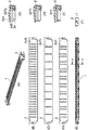
【図1】本発明の一実施の形態例のレセプタクルコネクタの諸図であり、(A)は斜視図、(B)は基板に搭載された状態の斜視図、(C)は平面図、(D)は正面図、(E)は側面図、(F)は(D)における線A−Aによる断面図を、それぞれ示す。
【図2】前方から後方の方向へ凹部が設けられた同レセプタクルコネクタの諸図であり、(A)は斜視図、(B)は平面図、(C)は一設計変更例の平面図、(D)は他の設計変更例の平面図、(E)は正面図、(F)は側面図、(G)は(E)における線A−Aによる断面図、(H)は(E)における線A−Aによる一設計変更例の断面図、(I)は(E)における線A−Aによる他の設計変更例の断面図を、それぞれ示す。
【図3】前方から後方の方向へ凸部が設けられた同レセプタクルコネクタの諸図であり、(A)は斜視図、(B)は平面図、(C)は一設計変更例の平面図、(D)は他の設計変更例の平面図、(E)は正面図、(F)は側面図、(G)は(E)における線A−Aによる断面図、(H)は(E)における線A−Aによる一設計変更例の断面図、(I)は(E)における線A−Aによる他の設計変更例の断面図を、それぞれ示す。
【図4】長手方向に凸部が設けられた同レセプタクルコネクタの諸図であり、(A)は斜視図、(B)は平面図、(C)は一設計変更例の平面図、(D)は他の設計変更例の平面図、(E)は正面図、(F)は側面図、(G)は(E)における線A−Aによる断面図を、それぞれ示す。
【図5】前方から後方の方向と長手方向に凹部と凸部が組合せて設けられた同レセプタクルコネクタの諸設計変更例の平面図を、(A)〜(C)にそれぞれ示す。
【図6】従来のレセプタクルコネクタの諸図であり、(A)は斜視図、(B)は平面図、(C)は正面図、(D)は側面図、(E)は(C)における線A−Aによる断面図、(F)は(C)における円内の拡大図を、それぞれ示す。
【図7】同レセプタクルコネクタの嵌合部が変形した状態を示す拡大正面図である。
【符号の説明】
1 レセプタクルコネクタ
2 インシュレータ
2a 嵌合部
2a1 上面
2a1a〜2a1f 凹部(溝等の肉抜き形状部)
2a1g〜2a1w 凸部(リブ等の肉盛り形状部)
2a2 下面
2b 基部(圧入部)
3 信号コンタクト
4 グラウンドコンタクト
5 シェル[0001]
BACKGROUND OF THE INVENTION
The present invention relates to a connector for mounting on a substrate, and more particularly to a structure for preventing deformation of a side wall portion of an insulator made of anisotropic resin in a connector during reflow heating or the like. A typical example of the anisotropic resin is a liquid crystal polymer (LCP).
[0002]
[Prior art]
As an example, a connector insulator used in a liquid crystal display (LCD) monitor has a complicated shape and is injection-molded. As the insulator material, a liquid crystal polymer that is excellent in heat resistance and hardly changes over time is mainly used. Since the liquid crystal polymer has anisotropy, it has a property of expanding and contracting according to the orientation of the material by heating and cooling at a high temperature.
[0003]
As shown in FIG. 6, since the shape of the
[0004]
Further, the
[0005]
Further, the upper surface 22a1 of the
[0006]
In addition, when manufacturing insulators such as connectors by injection molding glass fiber reinforced liquid crystal polymer, a manufacturing method that realizes a shape design with less warping during molding by predicting the influence of the unit structure that contributes to warping Has been proposed (see, for example, Patent Document 1).
[0007]
Further, a convex portion is formed on one of the pair of molds, and when the molten liquid crystal polyester resin is filled in the mold and the solidified liquid crystal polyester resin is then taken out from the mold, a molded product (connector of the connector) is formed. Insulators etc.) can be obtained, and a manufacturing method that can reduce the warpage of the molded product has also been proposed (see, for example, Patent Document 2).
[0008]
[Patent Document 1]
Japanese Laid-Open Patent Publication No. 5-228756
[Patent Document 2]
JP 2001-88173 A [0010]
[Problems to be solved by the invention]
Accordingly, the present invention aims to provide a board-mounting connector that improves the drawbacks of the conventional connector and is unlikely to cause heat-induced deformation in an anisotropic resin insulator during reflow or the like. is there.
[0011]
[Means for Solving the Problems]
The present invention employs the following means in order to solve the above problems.
[0012]
1. In the board mounting connector having a plurality of contacts and an insulator made of an anisotropic resin for holding each contact, the insulator is formed in a substantially L-shaped cross section, and one of the substantially L-shaped is each of the contacts. The other side of the substantially L-shape is a side wall portion that constitutes a fitting portion that fits with the mating connector, and the plurality of recesses formed on the inner surface of the side wall portion include the contacts. Are formed, and the plurality of concave portions and the convex portions are alternately formed by forming the plurality of convex portions by the plurality of concave portions, and the concave portions and the convex portions are formed on the outer surface of the side wall portion. Convex portions or concave portions are formed at portions corresponding to positions where the contact portions are alternately formed, each concave portion of the outer surface of the side wall portion is formed in a long groove shape in the longitudinal direction of each contact, and the side wall portion is With substrate By the connector to direction it is mounted on the substrate, substrate for mounting connectors that deformation of the side wall portion during reflow is prevented.
[0013]
2. 2. The board mounting connector according to 1, wherein the convex portion and the concave portion are formed on the outer surface of the side wall portion in combination.
[0014]
DETAILED DESCRIPTION OF THE INVENTION
A connector according to an embodiment of the present invention will be described with reference to FIGS. This connector is a receptacle connector mounted on a substrate inside the liquid crystal display monitor. The mating connector with which the receptacle connector is fitted is a relay connector with a flexible printed circuit (FPC) or a relay connector connected with a thin cable.
[0015]
As shown in FIG. 1, the
[0016]
Since the
[0017]
As shown in FIG. 2, since the shape of the
[0018]
Further, the
[0019]
Further, the upper surface 2a1 of the
[0020]
Thus, as described below, various modifications can be made to the shape of the
[0021]
(1) As shown in FIG. 2 (G), from the front to the rear of the upper surface 2a1 of the
[0022]
(2) The design of the recess 2a1a in (1) can be changed to a recess 2a1b having a step as shown in FIG. 2 (H).
[0023]
(3) The design of the concave portion 2a1a in (1) is changed to two concave portions 2a1c formed in series at a position facing one convex portion (rib) of the lower surface 2a2, as shown in FIG. 2 (I). can do.
[0024]
(4) As shown in FIG. 2B, the recess 2a1a in (1) is formed into a recess 2a1d formed in parallel at all locations on the upper surface 2a1 facing the plurality of protrusions (ribs) on the lower surface 2a2. The design can be changed. Alternatively, as shown in FIGS. 2C and 2D, the design can be changed to the recesses 2a1e and 2a1f formed in parallel at one place on the upper surface 2a1 facing each of the plurality of protrusions (ribs). .
[0025]
(5) As shown in FIG. 3G, a convex portion (rib) is formed at a position facing the concave portion of the lower surface 2a2 into which the
[0026]
(6) As shown in FIG. 3H, the design of the convex portion 2a1g in (5) above can be changed to a convex portion 2a1h having a step.
[0027]
(7) The convex portion 2a1g in (5) can be redesigned to two convex portions 2a1i formed in series at positions facing the concave portion of the lower surface 2a2, as shown in FIG. 3 (I). .
[0028]
(8) The design of the convex portion 2a1g in the above (5) is changed to a convex portion 2a1j formed in parallel at all locations on the upper surface 2a1 facing the plurality of concave portions on the lower surface 2a2, as shown in FIG. can do. Alternatively, as shown in FIGS. 3C and 3D, the design can be changed to convex portions 2a1k and 2a1l formed in parallel at one place on the upper surface 2a1 facing each of the plurality of concave portions.
[0029]
(9) When a convex portion 2a1m extending in the longitudinal direction is provided on the upper surface 2a1 of the
[0030]
(10) The convex portion 2a1m in (9) can be redesigned into two convex portions 2a1n and 2a1o extending in the longitudinal direction, as shown in FIG. 4C.
[0031]
(11) The two convex portions 2a1n and 2a1o in (10) are designed to be interrupted at two locations to form six convex portions 2a1p to 2a1u, as shown in FIG. 4D. Can be changed.
[0032]
(12) The design of the projection 2a1m in (9) can be changed to interrupt and form two projections 2a1v and 2a1w as shown in FIG. 4 (E).
[0033]
(13) As shown in FIG. 5, a concave portion and a convex portion can be provided in combination on the
[0034]
In the present embodiment, a plurality of concave portions and a plurality of convex portions are formed on the lower surface 2a2 of the side wall portion constituting the
[0035]
【The invention's effect】
As is apparent from the above description, the following effects are achieved according to the present invention.
[0036]
1. A concave portion (a hollow shape portion such as a groove) is provided at a position facing the convex portion (a build-up shape portion such as a rib) on the inner surface from the front to the rear of the outer surface of the fitting portion of the insulator made of anisotropic resin. As a result, irregularities similar to the inner surface are formed. Therefore, since the orientation balance becomes uniform, deformation of the fitting portion of the insulator due to the difference in thermal expansion coefficient is prevented.
[0037]
2. By providing a convex portion at a position facing the concave portion of the inner surface into which the contact is inserted from the front to the rear of the outer surface of the fitting portion of the insulator made of anisotropic resin, the same irregularities as the inner surface are formed. Therefore, since the orientation balance becomes uniform, deformation of the fitting portion of the insulator due to the difference in thermal expansion coefficient is prevented.
[0038]
3. By providing a convex portion extending in the longitudinal direction on the outer surface of the fitting portion of the insulator made of anisotropic resin, the resin is easily filled in the mold at the time of injection molding. As a result, the residual stress of the molded product is reduced, and deformation of the molded product due to stress relaxation during heating is prevented.
[Brief description of the drawings]
1A and 1B are views of a receptacle connector according to an embodiment of the present invention, in which FIG. 1A is a perspective view, FIG. 1B is a perspective view in a state of being mounted on a substrate, FIG. D) is a front view, (E) is a side view, and (F) is a sectional view taken along line AA in (D).
FIGS. 2A and 2B are views of the receptacle connector provided with a recess from the front to the rear, where FIG. 2A is a perspective view, FIG. 2B is a plan view, and FIG. 2C is a plan view of one design change example; (D) is a plan view of another design modification example, (E) is a front view, (F) is a side view, (G) is a sectional view taken along line AA in (E), and (H) is (E). Sectional drawing of the one design change example by line AA in FIG. 1, (I) shows sectional drawing of the other design change example by line AA in (E), respectively.
FIGS. 3A and 3B are views of the receptacle connector provided with a convex portion from the front to the rear, where FIG. 3A is a perspective view, FIG. 3B is a plan view, and FIG. 3C is a plan view of a design change example; , (D) is a plan view of another design modification example, (E) is a front view, (F) is a side view, (G) is a cross-sectional view taken along line AA in (E), and (H) is (E). ) Shows a cross-sectional view of one design change example taken along line AA in FIG. 9A, and FIG. 11I shows a cross-sectional view of another design change example taken along line AA in FIG.
FIGS. 4A and 4B are views of the receptacle connector provided with a convex portion in the longitudinal direction, wherein FIG. 4A is a perspective view, FIG. 4B is a plan view, and FIG. 4C is a plan view of one design change example; ) Is a plan view of another design modification example, (E) is a front view, (F) is a side view, and (G) is a sectional view taken along line AA in (E).
FIGS. 5A to 5C show plan views of various design changes of the receptacle connector in which concave portions and convex portions are provided in combination from the front to the rear and in the longitudinal direction.
6A and 6B are views of a conventional receptacle connector, where FIG. 6A is a perspective view, FIG. 6B is a plan view, FIG. 6C is a front view, FIG. 6D is a side view, and FIG. Sectional drawing by line AA, (F) shows the enlarged view in a circle in (C), respectively.
FIG. 7 is an enlarged front view showing a state where the fitting portion of the receptacle connector is deformed.
[Explanation of symbols]
DESCRIPTION OF
2a1g-2a1w Convex part (build-up shape part such as rib)
3 Signal contact 4
Claims (2)
前記インシュレータは、断面略L字状に形成され、前記略L字状の一方は前記各コンタクトを保持する基部となり、前記略L字状の他方は相手側コネクタと嵌合する嵌合部を構成する側壁部となり、
前記側壁部の内面に形成されている複数の凹部には、前記各コンタクトが収容され、前記複数の凹部により複数の凸部が形成されることによって前記各凹部と前記各凸部とが交互に形成され、前記側壁部の外面には、前記各凹部と前記各凸部とが交互に形成された位置に対応する部分に凸部又は凹部が形成され、
前記側壁部の外面の前記各凹部は、前記各コンタクトの長手方向に長い溝状に形成され、
前記側壁部が基板と対向するように前記コネクタが前記基板に搭載されることによって、リフローの際の前記側壁部の変形が防止されることを特徴とする基板搭載用コネクタ。In the board mounting connector having a plurality of contacts and an insulator made of anisotropic resin for holding each contact,
The insulator is formed to have a substantially L-shaped cross section, and one of the substantially L-shaped forms a base for holding the contacts, and the other of the substantially L-shaped forms a fitting portion that fits with a mating connector. The side wall
Each of the contacts is accommodated in a plurality of recesses formed on the inner surface of the side wall, and a plurality of projections are formed by the plurality of recesses, whereby the recesses and the projections are alternately formed. Formed on the outer surface of the side wall portion, a convex portion or a concave portion is formed in a portion corresponding to a position where the concave portions and the convex portions are alternately formed ,
Each of the recesses on the outer surface of the side wall is formed in a long groove shape in the longitudinal direction of each contact,
A board mounting connector, wherein the connector is mounted on the board so that the side wall faces the board, thereby preventing deformation of the side wall during reflow.
Priority Applications (7)
| Application Number | Priority Date | Filing Date | Title |
|---|---|---|---|
| JP2002331045A JP3778555B2 (en) | 2002-11-14 | 2002-11-14 | Board mounting connector |
| KR1020030080111A KR100567590B1 (en) | 2002-11-14 | 2003-11-13 | Electrical connector |
| CNB2003101149886A CN1294679C (en) | 2002-11-14 | 2003-11-14 | Electric connector |
| US10/712,339 US6913488B2 (en) | 2002-11-14 | 2003-11-14 | Electrical connector |
| DE60303548T DE60303548T2 (en) | 2002-11-14 | 2003-11-14 | Electrical connector |
| EP03026248A EP1420478B1 (en) | 2002-11-14 | 2003-11-14 | Electrical connector |
| TW092131907A TWI241750B (en) | 2002-11-14 | 2003-11-14 | Electrical connector |
Applications Claiming Priority (1)
| Application Number | Priority Date | Filing Date | Title |
|---|---|---|---|
| JP2002331045A JP3778555B2 (en) | 2002-11-14 | 2002-11-14 | Board mounting connector |
Publications (2)
| Publication Number | Publication Date |
|---|---|
| JP2004165049A JP2004165049A (en) | 2004-06-10 |
| JP3778555B2 true JP3778555B2 (en) | 2006-05-24 |
Family
ID=32171401
Family Applications (1)
| Application Number | Title | Priority Date | Filing Date |
|---|---|---|---|
| JP2002331045A Expired - Lifetime JP3778555B2 (en) | 2002-11-14 | 2002-11-14 | Board mounting connector |
Country Status (7)
| Country | Link |
|---|---|
| US (1) | US6913488B2 (en) |
| EP (1) | EP1420478B1 (en) |
| JP (1) | JP3778555B2 (en) |
| KR (1) | KR100567590B1 (en) |
| CN (1) | CN1294679C (en) |
| DE (1) | DE60303548T2 (en) |
| TW (1) | TWI241750B (en) |
Cited By (1)
| Publication number | Priority date | Publication date | Assignee | Title |
|---|---|---|---|---|
| WO2017126507A1 (en) * | 2016-01-18 | 2017-07-27 | タイコエレクトロニクスジャパン合同会社 | Connector housing |
Families Citing this family (22)
| Publication number | Priority date | Publication date | Assignee | Title |
|---|---|---|---|---|
| TWM273863U (en) * | 2004-12-03 | 2005-08-21 | Hon Hai Prec Ind Co Ltd | Electrical connector |
| TWI276256B (en) * | 2005-05-23 | 2007-03-11 | P Two Ind Inc | Electric connector with reinforced clamping performance |
| TWM288453U (en) * | 2005-09-05 | 2006-03-01 | P Two Ind Inc | Electrical connector structure |
| CN2840353Y (en) * | 2005-10-13 | 2006-11-22 | 富士康(昆山)电脑接插件有限公司 | Electric Connector |
| CN2850023Y (en) * | 2005-11-04 | 2006-12-20 | 富士康(昆山)电脑接插件有限公司 | Electric connector |
| TWI285011B (en) * | 2006-02-17 | 2007-08-01 | Chief Land Electronic Co Ltd | Method of fabricating connector |
| CN2909595Y (en) * | 2006-02-21 | 2007-06-06 | 富士康(昆山)电脑接插件有限公司 | electrical connector |
| US7387534B2 (en) * | 2006-03-15 | 2008-06-17 | Lotes Co., Ltd. | Electrical connector |
| CN2909599Y (en) * | 2006-05-29 | 2007-06-06 | 富士康(昆山)电脑接插件有限公司 | electrical connector |
| TWI320456B (en) * | 2006-12-29 | 2010-02-11 | Ind Tech Res Inst | Scroll type compressor |
| JP4494441B2 (en) * | 2007-07-03 | 2010-06-30 | 日本航空電子工業株式会社 | Electrical connector |
| USD605129S1 (en) * | 2007-12-27 | 2009-12-01 | Honda Tsushin Kogyo Co., Ltd. | Electrical cable connector |
| JP5044510B2 (en) | 2008-06-03 | 2012-10-10 | 株式会社東芝 | Housing, electronic device, and manufacturing method of housing |
| JP4772100B2 (en) * | 2008-10-28 | 2011-09-14 | 第一精工株式会社 | Insert molding apparatus and insert molding method |
| JP5293419B2 (en) * | 2009-06-04 | 2013-09-18 | 住友電装株式会社 | connector |
| CN101997217B (en) * | 2009-08-10 | 2012-12-19 | 富士康(昆山)电脑接插件有限公司 | Electric connector |
| JP5063659B2 (en) * | 2009-10-20 | 2012-10-31 | 日本航空電子工業株式会社 | connector |
| JP2012199065A (en) * | 2011-03-22 | 2012-10-18 | Sumitomo Chemical Co Ltd | Manufacturing method of fpc connector |
| WO2013059574A1 (en) * | 2011-10-19 | 2013-04-25 | Winchester Electronics Corporation | Closed entry din jack and connector with pcb board lock |
| TWI488376B (en) * | 2012-09-27 | 2015-06-11 | Ya Ping Lin | Electrical connector |
| JP6053019B2 (en) * | 2013-05-13 | 2016-12-27 | パナソニック株式会社 | Analysis method for hot warpage of liquid crystal polymer injection molded products |
| JP2020068168A (en) * | 2018-10-26 | 2020-04-30 | 株式会社オートネットワーク技術研究所 | connector |
Family Cites Families (17)
| Publication number | Priority date | Publication date | Assignee | Title |
|---|---|---|---|---|
| US5245454A (en) | 1991-12-31 | 1993-09-14 | At&T Bell Laboratories | Lcd display with microtextured back reflector and method for making same |
| JPH05228956A (en) * | 1992-02-20 | 1993-09-07 | Polyplastics Co | Manufacture of slender article |
| JP2502596Y2 (en) * | 1994-01-17 | 1996-06-26 | 日本エー・エム・ピー株式会社 | Electrical connector assembly |
| DE69609644T2 (en) | 1995-02-22 | 2000-12-28 | The Whitaker Corp., Wilmington | PCMCIA input / output card connector |
| JP3023276U (en) * | 1995-09-07 | 1996-04-16 | モレックス インコーポレーテッド | Electrical connector |
| TW532599U (en) * | 2002-04-18 | 2003-05-11 | Hon Hai Prec Ind Co Ltd | Electrical connector |
| JPH10321077A (en) * | 1997-05-19 | 1998-12-04 | Alps Electric Co Ltd | Electrical component and attaching structure of the same electrical component |
| JPH11111421A (en) * | 1997-10-02 | 1999-04-23 | Fujitsu Ltd | Connector holding plate and method of manufacturing connector holding plate |
| JP3273024B2 (en) * | 1998-08-27 | 2002-04-08 | 日本圧着端子製造株式会社 | IDC type electrical connector and its assembly |
| US6176748B1 (en) * | 1998-11-24 | 2001-01-23 | Molex Incorporated | Terminal positioning system |
| DE19909847A1 (en) * | 1999-03-07 | 2000-09-14 | Interconnectron Gmbh | Method of manufacturing multi-pin electrical connector halves |
| JP4481400B2 (en) * | 1999-09-22 | 2010-06-16 | 住友化学株式会社 | Method for producing molded body made of liquid crystal polyester resin and method for producing connector part |
| JP3569843B2 (en) * | 2000-05-01 | 2004-09-29 | 日本航空電子工業株式会社 | Surface mount connector |
| JP2001336611A (en) * | 2000-05-25 | 2001-12-07 | Enplas Corp | Mold gear |
| US6354886B1 (en) * | 2000-09-08 | 2002-03-12 | Advanced Connecteck Inc. | Electrical connector |
| US6537086B1 (en) * | 2001-10-15 | 2003-03-25 | Hon Hai Precision Ind. Co., Ltd. | High speed transmission electrical connector with improved conductive contact |
| US6619986B1 (en) * | 2002-04-19 | 2003-09-16 | Hon Hai Precision Ind. Co., Ltd. | Electrical connector with metal shield |
-
2002
- 2002-11-14 JP JP2002331045A patent/JP3778555B2/en not_active Expired - Lifetime
-
2003
- 2003-11-13 KR KR1020030080111A patent/KR100567590B1/en not_active Expired - Lifetime
- 2003-11-14 DE DE60303548T patent/DE60303548T2/en not_active Expired - Lifetime
- 2003-11-14 TW TW092131907A patent/TWI241750B/en not_active IP Right Cessation
- 2003-11-14 US US10/712,339 patent/US6913488B2/en not_active Expired - Lifetime
- 2003-11-14 CN CNB2003101149886A patent/CN1294679C/en not_active Expired - Lifetime
- 2003-11-14 EP EP03026248A patent/EP1420478B1/en not_active Expired - Lifetime
Cited By (5)
| Publication number | Priority date | Publication date | Assignee | Title |
|---|---|---|---|---|
| WO2017126507A1 (en) * | 2016-01-18 | 2017-07-27 | タイコエレクトロニクスジャパン合同会社 | Connector housing |
| JP2017130257A (en) * | 2016-01-18 | 2017-07-27 | タイコエレクトロニクスジャパン合同会社 | Connector housing |
| CN108432058A (en) * | 2016-01-18 | 2018-08-21 | 泰科电子日本合同会社 | Connector shell |
| CN108432058B (en) * | 2016-01-18 | 2019-10-01 | 泰科电子日本合同会社 | Connector shell |
| US10553983B2 (en) | 2016-01-18 | 2020-02-04 | Tyco Electronics Japan G.K. | Connector housing with a reduced warpage |
Also Published As
| Publication number | Publication date |
|---|---|
| US6913488B2 (en) | 2005-07-05 |
| TW200501517A (en) | 2005-01-01 |
| DE60303548D1 (en) | 2006-04-20 |
| TWI241750B (en) | 2005-10-11 |
| JP2004165049A (en) | 2004-06-10 |
| EP1420478B1 (en) | 2006-02-15 |
| CN1294679C (en) | 2007-01-10 |
| EP1420478A1 (en) | 2004-05-19 |
| DE60303548T2 (en) | 2006-08-24 |
| CN1503409A (en) | 2004-06-09 |
| KR20040042862A (en) | 2004-05-20 |
| US20040097107A1 (en) | 2004-05-20 |
| KR100567590B1 (en) | 2006-04-05 |
Similar Documents
| Publication | Publication Date | Title |
|---|---|---|
| JP3778555B2 (en) | Board mounting connector | |
| TWI641190B (en) | Electrical connector and production method thereof | |
| CA2369688C (en) | Contact assembly for a plug connector, in particular for a pcb plug connector | |
| CN104604041B (en) | waterproof connector | |
| CN111129828B (en) | Substrate connector and method for manufacturing housing of substrate connector | |
| US6068523A (en) | Circuit molded structure having bus bars forming internal circuits | |
| JP5063659B2 (en) | connector | |
| JP5486885B2 (en) | Electrical connectors and connectors | |
| CN115053408A (en) | Connector housing, method for producing the same and mold for use in the method | |
| JP5376784B2 (en) | Connector for flexible printed circuit board | |
| CN111138074A (en) | Glass product forming die, forming equipment and processing method | |
| EP1139499B1 (en) | Electrical connector | |
| KR102503959B1 (en) | Plugs can be manufactured more simply using injection molding | |
| JP4409782B2 (en) | Molding method of resin crowning gear molding | |
| TW202324853A (en) | Waterproof connector | |
| KR100531219B1 (en) | Injection molding method of terminal inserted plastic mold and inserting terminal | |
| JP6881996B2 (en) | connector | |
| JP3812930B2 (en) | SMT connector | |
| CN1307750C (en) | Electric connector | |
| CN119581913A (en) | Connectors | |
| JP2003282172A (en) | Connector for printed wiring board | |
| JP2024107885A (en) | connector | |
| JP2024107853A (en) | connector | |
| WO2025231928A1 (en) | Horizontal connector | |
| CN1838403B (en) | Housing for housing solid-state imaging device and solid-state imaging device |
Legal Events
| Date | Code | Title | Description |
|---|---|---|---|
| A977 | Report on retrieval |
Free format text: JAPANESE INTERMEDIATE CODE: A971007 Effective date: 20041109 |
|
| A131 | Notification of reasons for refusal |
Free format text: JAPANESE INTERMEDIATE CODE: A131 Effective date: 20041124 |
|
| A521 | Request for written amendment filed |
Free format text: JAPANESE INTERMEDIATE CODE: A523 Effective date: 20050121 |
|
| A131 | Notification of reasons for refusal |
Free format text: JAPANESE INTERMEDIATE CODE: A131 Effective date: 20050427 |
|
| A521 | Request for written amendment filed |
Free format text: JAPANESE INTERMEDIATE CODE: A523 Effective date: 20050624 |
|
| A131 | Notification of reasons for refusal |
Free format text: JAPANESE INTERMEDIATE CODE: A131 Effective date: 20051130 |
|
| A521 | Request for written amendment filed |
Free format text: JAPANESE INTERMEDIATE CODE: A523 Effective date: 20060125 |
|
| TRDD | Decision of grant or rejection written | ||
| A01 | Written decision to grant a patent or to grant a registration (utility model) |
Free format text: JAPANESE INTERMEDIATE CODE: A01 Effective date: 20060222 |
|
| A61 | First payment of annual fees (during grant procedure) |
Free format text: JAPANESE INTERMEDIATE CODE: A61 Effective date: 20060227 |
|
| R150 | Certificate of patent or registration of utility model |
Ref document number: 3778555 Country of ref document: JP Free format text: JAPANESE INTERMEDIATE CODE: R150 Free format text: JAPANESE INTERMEDIATE CODE: R150 |
|
| FPAY | Renewal fee payment (event date is renewal date of database) |
Free format text: PAYMENT UNTIL: 20090310 Year of fee payment: 3 |
|
| FPAY | Renewal fee payment (event date is renewal date of database) |
Free format text: PAYMENT UNTIL: 20100310 Year of fee payment: 4 |
|
| FPAY | Renewal fee payment (event date is renewal date of database) |
Free format text: PAYMENT UNTIL: 20100310 Year of fee payment: 4 |
|
| FPAY | Renewal fee payment (event date is renewal date of database) |
Free format text: PAYMENT UNTIL: 20100310 Year of fee payment: 4 |
|
| FPAY | Renewal fee payment (event date is renewal date of database) |
Free format text: PAYMENT UNTIL: 20110310 Year of fee payment: 5 |
|
| R250 | Receipt of annual fees |
Free format text: JAPANESE INTERMEDIATE CODE: R250 |
|
| FPAY | Renewal fee payment (event date is renewal date of database) |
Free format text: PAYMENT UNTIL: 20110310 Year of fee payment: 5 |
|
| FPAY | Renewal fee payment (event date is renewal date of database) |
Free format text: PAYMENT UNTIL: 20120310 Year of fee payment: 6 |
|
| R250 | Receipt of annual fees |
Free format text: JAPANESE INTERMEDIATE CODE: R250 |
|
| FPAY | Renewal fee payment (event date is renewal date of database) |
Free format text: PAYMENT UNTIL: 20120310 Year of fee payment: 6 |
|
| FPAY | Renewal fee payment (event date is renewal date of database) |
Free format text: PAYMENT UNTIL: 20120310 Year of fee payment: 6 |
|
| FPAY | Renewal fee payment (event date is renewal date of database) |
Free format text: PAYMENT UNTIL: 20130310 Year of fee payment: 7 |
|
| R250 | Receipt of annual fees |
Free format text: JAPANESE INTERMEDIATE CODE: R250 |
|
| FPAY | Renewal fee payment (event date is renewal date of database) |
Free format text: PAYMENT UNTIL: 20130310 Year of fee payment: 7 |
|
| FPAY | Renewal fee payment (event date is renewal date of database) |
Free format text: PAYMENT UNTIL: 20130310 Year of fee payment: 7 |
|
| FPAY | Renewal fee payment (event date is renewal date of database) |
Free format text: PAYMENT UNTIL: 20140310 Year of fee payment: 8 |
|
| R250 | Receipt of annual fees |
Free format text: JAPANESE INTERMEDIATE CODE: R250 |
|
| R250 | Receipt of annual fees |
Free format text: JAPANESE INTERMEDIATE CODE: R250 |
|
| R250 | Receipt of annual fees |
Free format text: JAPANESE INTERMEDIATE CODE: R250 |
|
| R250 | Receipt of annual fees |
Free format text: JAPANESE INTERMEDIATE CODE: R250 |
|
| R250 | Receipt of annual fees |
Free format text: JAPANESE INTERMEDIATE CODE: R250 |
|
| R250 | Receipt of annual fees |
Free format text: JAPANESE INTERMEDIATE CODE: R250 |
|
| R250 | Receipt of annual fees |
Free format text: JAPANESE INTERMEDIATE CODE: R250 |
|
| R250 | Receipt of annual fees |
Free format text: JAPANESE INTERMEDIATE CODE: R250 |
|
| R250 | Receipt of annual fees |
Free format text: JAPANESE INTERMEDIATE CODE: R250 |
|
| R250 | Receipt of annual fees |
Free format text: JAPANESE INTERMEDIATE CODE: R250 |
|
| EXPY | Cancellation because of completion of term |