JP3785196B2 - Image processing device - Google Patents
Image processing device Download PDFInfo
- Publication number
- JP3785196B2 JP3785196B2 JP14518294A JP14518294A JP3785196B2 JP 3785196 B2 JP3785196 B2 JP 3785196B2 JP 14518294 A JP14518294 A JP 14518294A JP 14518294 A JP14518294 A JP 14518294A JP 3785196 B2 JP3785196 B2 JP 3785196B2
- Authority
- JP
- Japan
- Prior art keywords
- image data
- image
- memory
- switch
- data
- Prior art date
- Legal status (The legal status is an assumption and is not a legal conclusion. Google has not performed a legal analysis and makes no representation as to the accuracy of the status listed.)
- Expired - Fee Related
Links
- 230000015654 memory Effects 0.000 claims description 73
- 238000004364 calculation method Methods 0.000 claims description 6
- 238000006243 chemical reaction Methods 0.000 claims description 2
- 238000010586 diagram Methods 0.000 description 11
- 238000000034 method Methods 0.000 description 4
- 238000003705 background correction Methods 0.000 description 1
- 238000013500 data storage Methods 0.000 description 1
- 238000003384 imaging method Methods 0.000 description 1
- 238000012544 monitoring process Methods 0.000 description 1
- 238000003672 processing method Methods 0.000 description 1
Images


Landscapes
- Image Processing (AREA)
Description
【0001】
【産業上の利用分野】
本発明は、画像処理装置に関するものである。
【0002】
【従来の技術】
従来、画像処理装置において、画像データの2値化処理を行う場合、図9に示すようにTVカメラ1からのアナログの画像信号と、例えば8ビットからなる基準値2をD/A変換器3でアナログ変換した基準信号とをアナログ比較器4で比較して、画像信号のレベルが基準信号のレベルを越えるか否かの比較結果に応じた1ビットの出力を得、この1ビットのデータを2値化メモリ5に取り込むようにする方法や、或いは図10に示すようにTVカメラ1からのアナログの画像信号をA/D変換器6で例えば8ビットの画像データに変換し、この変換した画像データと8ビットからなる基準値2とを加算器7で加算演算して9ビットのデータを得、このデジタル値をデジタル比較器8により所定値と比較して1ビットの出力を得、この1ビットのデータを2値化メモリ5に取り込むようにする方法が広く採用されている。
【0003】
【発明が解決しようとする課題】
しかし、上記のような一定の閾値比較による2値化処理方法では、任意の特定の明るさを持つ画像データ部分の2値化処理や、TVカメラの視野内の明るさむらを補正するシェーディング補正2値化処理等の多様な2値化処理には対応できない。また同一のハードウェアを用いて多様な2値化処理を行う装置も無かった。
【0004】
本発明は上記問題点に鑑みて為されたもので、その目的とするところは、一つのハードウェアにより多様な2値化処理が可能な画像処理装置を提供するにある。
【0005】
【課題を解決するための手段】
上記目的を達成するために請求項1の発明では、TVカメラと、TVカメラから出力される画像信号をA/D変換するA/D変換器と、読み書き可能な画像データ格納用濃淡メモリと、前記A/D変換器でA/D変換された画像データと前記画像格納用濃淡メモリに書き込まれた画像データとを組み合わせ選択して演算処理を行う演算手段と、該演算手段から出力される画像データを読み出しアドレスとしてそのアドレスに予め書き込まれている1ビットデータを出力するルックアップテーブルメモリと、前記画像データ格納用濃淡メモリの画像データが前記演算手段に対して取り込まれるのをオンオフする第1のスイッチと、前記A/D変換器からの画像データが前記演算手段に対して取り込まれるのオンオフする第2のスイッチとを備え、前記ルックアップテーブルメモリに書き込まれる1ビットデータは2値化処理の目的に応じて任意に設定され、濃淡画像の2値化処理を行う場合には前記第1のスイッチをオフするとともに前記第2のスイッチをオンして、前記演算手段に取り込む画像データを前記A/D変換器でA/D変換された画像データのみとし、前記TVカメラからの画像データを補正処理する場合には前記第1のスイッチをオンするとともに第2のスイッチをオンして、前記演算手段に取り込む画像データを、前記画像格納用濃淡メモリに予め書き込まれた補正パターンを持つ画像データ及び前記A/D変換器でA/D変換された画像データとして前記演算手段で両画像データの減算処理を行い、撮像対象が移動する物体の場合には前記第1のスイッチをオンするとともに前記第2のスイッチをオフして、前記A/D変換器でA/D変換された画像データを前記画像格納用濃淡メモリに書き込み、該画像格納用濃淡メモリに書き込まれた画像データを前記演算手段を通じて前記ルックアップテーブルメモリのアドレスを指定するデータとして用いるものである。
【0006】
請求項2の発明では、請求項1の発明において、前記ルックアップテーブルメモリに書き込まれる1ビットデータは、前記スイッチの切り替わりに応じて設定されるものである。
【0007】
【作用】
請求項1の発明によれば、画像データが読み出しアドレスとなるルックアップメモリに設定する1ビットデータを任意の明るさに対して任意に設定することにより特定の明るさを持つ画像データ部分の2値化処理が可能となり、しかも濃淡メモリからの画像データの演算手段への取り込みをオンオフする第1のスイッチを設けているので、TVカメラの画像信号に対する濃淡メモリの画像データの組み合わせが選択することができ、その上A/D変換器からの画像データの演算手段への取り込みをオンオフする第2のスイッチを設けているので、濃淡メモリからの画像データに対するTVカメラの画像信号の組み合わせも選択することができ、その結果通常の2値化は勿論のこと補正した2値化と、移動する撮像対象の物体の画像の2値化とを行うことが可能となり、多様な2値化処理が可能な画像処理装置を提供することができる。
【0008】
請求項2の発明によれば、前記スイッチの切り替わりに応じてそのときの2値化処理の目的に応じたデータ設定により、スイッチの切り替えで選択した画像データに最適な2値化が図れる。
【0009】
【実施例】
以下、本発明の実施例を、図面を参照して説明する。
【0010】
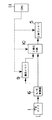
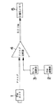
図2は本実施例装置のブロック図を示しており、本実施例装置は、TVカメラ1、A/D変換器6、濃淡メモリ9、2値化回路10、2値化メモリ5及び各部の制御、演算処理、更にメモリ5,9の読み書きの制御を行うCPU11で構成される。
【0011】
対象物体を撮像して得られるTVカメラ1のアナログの画像信号はA/D変換器6でA/D変換された後、濃淡画像データ(例えば8ビットのデータ)として濃淡メモリ9に格納されたり、直接2値化回路10へ送りこまれるようになっている。
【0012】
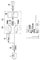
2値化回路10は8ビットの画像データを1ビットの2値化画像データに変換するためのもので、図1に示すように演算器12と、ルックアップテーブルメモリ13と、演算器12へ入力するデータを選択する第1のスイッチSWa及び第2のスイッチSWbからなる選択スイッチ部14とで構成されている。
【0013】
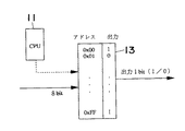
ルックアップテーブルメモリ13は、図3に示すように例えば8ビットの入力信号がアドレスとなり、そのアドレスに格納している1ビットデータが出力値として読み出されるようになっている。そしてCPU11からアドレスを指定することにより当該アドレスに格納する出力値を設定することができるようになっている。
【0014】
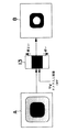
本実施例ではTVカメラ1により得られた図4に示す濃淡画像Aの内所定の明るさ部分に対して2値化処理を行うため、予めCPU11により明るさレベルが低いレベルの画像信号の8ビットデータ及び高レベルの画像信号の8ビットデータで指定されるルックアップテーブルメモリ13のアドレスには白(1)を、残りの中間の明るさレベルの画像信号の8ビットデータで指定されるアドレスには黒(0)を設定してある。
【0015】
而して本実施例によれば、図1に示すように選択スイッチ部13のスイッチSWaを濃淡メモリ9から切離し、スイッチSWbをA/D変換器6に接続することにより演算器12に取り込まれる画像データをA/D変換器6で変換された8ビットデータのみとし、このデータを演算器12を通じてルックアップテーブルメモリ13にアドレスとして与えると、その8ビットデータにより指定されるルックアップテーブルメモリ13のアドレスに設定されている1ビットデータが出力値として読み出されることになる。
【0016】
ここで上記の条件でルックアップテーブルメモリ13には1ビットデータが設定されているため、中間の明るさ部分のデータに対しては1、つまり白のデータが出力され、その他の部分のデータに対しては0、つまり黒のデータが出力されることになり、このデータが2値化メモリ5に取り込まれる。2値化メモリ5に取り込まれた2値化処理後の画像データにより画像を再生するとその出力画像Bは図4に示すように元の画像の中間の明るさ部分が黒く、その他の部分が白い2値化画像となる。
【0017】
次に、TVカメラ1の視野内の明るさむらが存在して、TVカメラ1からの画像データをそのまま2値化処理すると適切な2値化画像が得られない場合には何等かの補正処理を行う必要がある。この場合には図1に示す濃淡メモリ9に明るさむらを補正するために予め図6に示す補正パターンを持つ画像Dの画像データを登録しておく。そして選択スイッチ部13のスイッチSWaを図5に示すように濃淡メモリ9側に接続し、スイッチSWbをA/D変換器6側に接続してパータン画像データとTVカメラ1で撮像して得られた画像データAとを演算器12に入力し、演算器12で減算することにより、明るさむらCの部分が画像Dの補正パターンで相殺されることになる。この演算結果のデータをルックアップテーブルメモリ13にアドレスとして送ることにより、1ビットの出力が読み出されて明るさむらの影響の無い2値化データが得られることになる。ここでルックアップテーブルメモリ13では予め所定の明るさ以上のデータにより指定されるアドレスに白(1)のデータを、また所定の明るさより低いデータにより指定されるアドレスに黒(0)のデータを夫々CPU11によって設定されているため、出力画像Bは図6のような画像となる。
【0018】
ところでTVカメラ1で撮像する対象物体が落下物体等移動する物体の場合には、TVカメラ1で撮像した画像をモニタしながら2値化レベルの設定を行うことは困難である。このような場合にはCPU11の制御の下で、TVカメラ1で撮像した画像をA/D変換した後、A/D変換して得られた画像データを一旦濃淡メモリ9に取り込み、この取り込んだメモリ画像データに対して2値化レベルの設定を行うと容易にレベルの設定を行うことができる。
【0019】
この場合図7に示すように選択スイッチ部13のスイッチSWaを濃淡メモリ9側に接続し、スイッチSWbをA/D変換器6側から切離して濃淡メモリ9からのメモリ画像データのみを演算器12を通じてルックアップテーブルメモリ13に送り、ルックアップテーブルメモリ13のアドレスを指定するデータとする。
【0020】
図8はルックアップテーブルメモリ13の1ビットデータを図4の場合と同じように設定している例を示しており、濃淡メモリ9に取り込まれている画像Aの内中間の明るさ部分に対する2値化処理が為されて、出力画像Bは図4の場合と同じような2値化画像となる。以上のように本発明画像処理装置は、共通のハードウェアを持ち選択スイッチ部13の切り替え設定によって多様な2値化処理が行えるものである。
【0021】
尚上記実施例では画像データを8ビット構成とし、ルックアップテーブルメモリ13のアドレスを8ビットとしているが、特にこのビット数には限定されるものではない。
【0022】
【発明の効果】
請求項1の発明は、TVカメラと、TVカメラから出力される画像信号をA/D変換するA/D変換器と、読み書き可能な画像データ格納用濃淡メモリと、前記A/D変換器でA/D変換された画像データと前記画像格納用濃淡メモリに書き込まれた画像データとを組み合わせ選択して演算処理を行う演算手段と、該演算手段から出力される画像データを読み出しアドレスとしてそのアドレスに予め書き込まれている1ビットデータを出力するルックアップテーブルメモリと、前記画像データ格納用濃淡メモリの画像データが前記演算手段に対して取り込まれるのをオンオフする第1のスイッチと、前記A/D変換器からの画像データが前記演算手段に対して取り込まれるのオンオフする第2のスイッチとを備え、前記ルックアップテーブルメモリに書き込まれる1ビットデータは2値化処理の目的に応じて任意に設定され、濃淡画像の2値化処理を行う場合には前記第1のスイッチをオフするとともに前記第2のスイッチをオンして、前記演算手段に取り込む画像データを前記A/D変換器でA/D変換された画像データのみとし、前記TVカメラからの画像データを補正処理する場合には前記第1のスイッチをオンするとともに第2のスイッチをオンして、前記演算手段に取り込む画像データを、前記画像格納用濃淡メモリに予め書き込まれた補正パターンを持つ画像データ及び前記A/D変換器でA/D変換された画像データとして前記演算手段で両画像データの減算処理を行い、撮像対象が移動する物体の場合には前記第1のスイッチをオンするとともに前記第2のスイッチをオフして、前記A/D変換器でA/D変換された画像データを前記画像格納用濃淡メモリに書き込み、該画像格納用濃淡メモリに書き込まれた画像データを前記演算手段を通じて前記ルックアップテーブルメモリのアドレスを指定するデータとして用いるので、画像データが読み出しアドレスとなるルックアップメモリに設定する1ビットデータを任意の明るさに対して任意に設定することにより特定の明るさを持つ画像データ部分の2値化処理が可能となり、また濃淡メモリからの画像データの演算手段への取り込みをオンオフする第1のスイッチによって、TVカメラの画像信号に対する濃淡メモリの画像データの組み合わせが選択することができ、その上A/D変換器からの画像データの演算手段への取り込みをオンオフする第2のスイッチによって、濃淡メモリからの画像データに対するTVカメラの画像信号の組み 合わせも選択することができ、その結果通常の2値化は勿論のこと補正した2値化と、移動する撮像対象の物体の画像の2値化とを行うことが可能となり、多様な2値化処理が可能な画像処理装置を提供することができる。
【0023】
請求項2の発明は、前記ルックアップテーブルメモリに書き込まれる1ビットデータは、前記スイッチの切り替わりに応じて設定されるので、スイッチの切り替わりに応じてそのときの2値化処理の目的に応じたデータ設定により、スイッチの切り替えで選択した画像データに最適な2値化が図れる。
【図面の簡単な説明】
【図1】 本発明の実施例装置の2値化処理回路の一使用状態を示す回路構成図である。
【図2】 本発明の実施例装置全体のブロック図である。
【図3】 同上のルックアップテーブルメモリの概念図である。
【図4】 同上の使用例の2値化処理のイメージ図である。
【図5】 2値化処理回路の別の使用状態を示す回路構成図である。
【図6】 同上の使用例の2値化処理のイメージ図である。
【図7】 2値化処理回路の他の使用状態を示す回路構成図である。
【図8】 同上の使用例の2値化処理のイメージ図である。
【図9】 従来例のブロック図である。
【図10】 別の従来例のブロック図である。
【符号の説明】
1 TVカメラ
5 2値化メモリ
6 A/D変換器
9 濃淡メモリ
10 2値化処理回路
12 演算器
13 ルックアップテーブルメモリ
14 選択スイッチ部
SWa,SWb スイッチ[0001]
[Industrial application fields]
The present invention relates to an image processing apparatus.
[0002]
[Prior art]
Conventionally, in an image processing apparatus, when performing binarization processing for image data, and the analog image signal from the
[0003]
[Problems to be solved by the invention]
However, in the binarization processing method based on the constant threshold comparison as described above, the binarization processing of the image data portion having an arbitrary specific brightness and the shading correction for correcting the brightness unevenness in the field of view of the TV camera. It cannot cope with various binarization processing such as binarization processing. In addition, there is no device that performs various binarization processes using the same hardware.
[0004]
The present invention has been made in view of the above problems, and an object of the present invention is to provide an image processing apparatus capable of performing various binarization processes with a single piece of hardware.
[0005]
[Means for Solving the Problems]
In order to achieve the above object, according to the first aspect of the present invention, a TV camera, an A / D converter for A / D converting an image signal output from the TV camera, a readable / writable density memory for storing image data, arithmetic means for performing arithmetic processing said a / D converter in combination with the image data written in the shading memory for the image storage and a / D converted image data selected by the image output from said arithmetic means the on-off and a look-up table memory which outputs a 1-bit data written in advance in the address as a read address data, the image data of the image data storage shading memory from being taken with respect to the
[0006]
According to a second aspect of the present invention, in the first aspect of the invention, the 1-bit data written to the look-up table memory is set according to switching of the switch.
[0007]
[Action]
According to the first aspect of the present invention, 2 bits of the image data portion having a specific brightness can be obtained by arbitrarily setting 1-bit data set in the lookup memory from which the image data becomes a read address for an arbitrary brightness. binarization processing is possible, and since there is provided a first switch for turning on and off the uptake of computing means of the image data from the shading memory, the combination of the image data of the grayscale memory for the image signal of the TV camera to select In addition , since the second switch for turning on / off the loading of the image data from the A / D converter into the calculation means is provided, the combination of the TV camera image signal and the image data from the grayscale memory is also selected. As a result, the binarization corrected as well as the normal binarization, and the binarization of the image of the moving object to be imaged It becomes possible to carry out, it can be a variety of binarization to provide an image processing apparatus capable.
[0008]
According to the invention of
[0009]
【Example】
Hereinafter, an embodiment of the present invention will be described with reference to the drawings.
[0010]
Figure 2 shows a block diagram of the embodiment device, the embodiment device,
[0011]
An analog image signal of the
[0012]
The
[0013]
As shown in FIG. 3, in the
[0014]
In this embodiment, since the binarization process is performed on a predetermined brightness portion of the grayscale image A shown in FIG. 4 obtained by the
[0015]
Thus, according to the present embodiment, the switch SWa of the
[0016]
Here, since 1-bit data is set in the
[0017]
Next, if there is uneven brightness in the field of view of the
[0018]
By the way, when the target object imaged by the
[0019]
In this case, as shown in FIG. 7, the switch SWa of the
[0020]
FIG. 8 shows an example in which 1-bit data in the
[0021]
In the above embodiment, the image data has an 8-bit configuration and the address of the
[0022]
【The invention's effect】
The invention of
[0023]
According to the second aspect of the present invention, the 1-bit data written to the look-up table memory is set according to the switching of the switch. By the data setting, binarization optimal for the image data selected by switching the switch can be achieved.
[Brief description of the drawings]
FIG. 1 is a circuit configuration diagram showing one use state of a binarization processing circuit of an apparatus according to an embodiment of the present invention.
FIG. 2 is a block diagram of an entire apparatus according to an embodiment of the present invention.
FIG. 3 is a conceptual diagram of the lookup table memory of the above.
FIG. 4 is an image diagram of binarization processing in the above usage example.
FIG. 5 is a circuit configuration diagram showing another usage state of the binarization processing circuit.
FIG. 6 is an image diagram of binarization processing in the usage example.
FIG. 7 is a circuit configuration diagram showing another usage state of the binarization processing circuit.
FIG. 8 is an image diagram of binarization processing in the usage example.
FIG. 9 is a block diagram of a conventional example.
FIG. 10 is a block diagram of another conventional example.
[Explanation of symbols]
DESCRIPTION OF
Claims (2)
前記ルックアップテーブルメモリに書き込まれる1ビットデータは2値化処理の目的に応じて任意に設定され、
濃淡画像の2値化処理を行う場合には前記第1のスイッチをオフするとともに前記第2のスイッチをオンして、前記演算手段に取り込む画像データを前記A/D変換器でA/D変換された画像データのみとし、
前記TVカメラからの画像データを補正処理する場合には前記第1のスイッチをオンするとともに第2のスイッチをオンして、前記演算手段に取り込む画像データを、前記画像格納用濃淡メモリに予め書き込まれた補正パターンを持つ画像データ及び前記A/D変換器でA/D変換された画像データとして前記演算手段で両画像データの減算処理を行い、
撮像対象が移動する物体の場合には前記第1のスイッチをオンするとともに前記第2のスイッチをオフして、前記A/D変換器でA/D変換された画像データを前記画像格納用濃淡メモリに書き込み、該画像格納用濃淡メモリに書き込まれた画像データを前記演算手段を通じて前記ルックアップテーブルメモリのアドレスを指定するデータとして用いることを特徴とする画像処理装置。TV camera and an A / D converter for an image signal to A / D conversion output from the TV camera, a shading memory for storing image data read-write, the A / D converter in A / D converted image arithmetic means for performing arithmetic processing combining the image data written data and the image storing shading memory selected and are written in advance in the address as the read image data address output from the calculation means 1 A look-up table memory for outputting bit data; a first switch for turning on / off the image data stored in the image data storing gray-scale memory to be taken into the computing means; and image data from the A / D converter And a second switch for turning on and off that is taken into the computing means ,
The 1-bit data to be written into the look-up table memory is arbitrarily set depending on the purpose of the binarization processing,
When performing binarization processing of a grayscale image, the first switch is turned off and the second switch is turned on, and the A / D converter converts the image data to be taken into the arithmetic means by the A / D converter. Only the processed image data,
When the image data from the TV camera is corrected, the first switch is turned on and the second switch is turned on, and the image data to be taken into the computing means is written in the image storage density memory in advance. The image data having the corrected pattern and the image data A / D converted by the A / D converter are subjected to subtraction processing of both image data by the arithmetic means,
When the object to be imaged is a moving object, the first switch is turned on and the second switch is turned off, and the image data A / D converted by the A / D converter is used for the image storage density. An image processing apparatus using the image data written in a memory and the image data written in the gray memory for image storage as data for designating an address of the lookup table memory through the arithmetic means .
Priority Applications (1)
| Application Number | Priority Date | Filing Date | Title |
|---|---|---|---|
| JP14518294A JP3785196B2 (en) | 1994-06-27 | 1994-06-27 | Image processing device |
Applications Claiming Priority (1)
| Application Number | Priority Date | Filing Date | Title |
|---|---|---|---|
| JP14518294A JP3785196B2 (en) | 1994-06-27 | 1994-06-27 | Image processing device |
Publications (2)
| Publication Number | Publication Date |
|---|---|
| JPH0816769A JPH0816769A (en) | 1996-01-19 |
| JP3785196B2 true JP3785196B2 (en) | 2006-06-14 |
Family
ID=15379329
Family Applications (1)
| Application Number | Title | Priority Date | Filing Date |
|---|---|---|---|
| JP14518294A Expired - Fee Related JP3785196B2 (en) | 1994-06-27 | 1994-06-27 | Image processing device |
Country Status (1)
| Country | Link |
|---|---|
| JP (1) | JP3785196B2 (en) |
-
1994
- 1994-06-27 JP JP14518294A patent/JP3785196B2/en not_active Expired - Fee Related
Also Published As
| Publication number | Publication date |
|---|---|
| JPH0816769A (en) | 1996-01-19 |
Similar Documents
| Publication | Publication Date | Title |
|---|---|---|
| EP0297516B1 (en) | Picture signal binarization system | |
| US7239758B2 (en) | Signal processing device for reducing noise of image signal, signal processing program, and signal processing method | |
| JPH03248674A (en) | Half-tone picture processor | |
| JP3785196B2 (en) | Image processing device | |
| JPS63288565A (en) | Image processor | |
| JP3051144B2 (en) | Halftone image processing device | |
| JP3225099B2 (en) | Image processing device | |
| JPS5888969A (en) | Image sharpening processing method | |
| JPH0670162A (en) | Image correction device | |
| JP2502957B2 (en) | Image converter | |
| JP3135311B2 (en) | Image processing device | |
| JP3215146B2 (en) | Image processing device | |
| JP3466655B2 (en) | Image processing device | |
| JP2506205B2 (en) | Black level correction device | |
| JP3303990B2 (en) | Image signal processing device | |
| JP2521744B2 (en) | Image processing device | |
| JP3157870B2 (en) | Image processing method | |
| JP2857906B2 (en) | Halftone binarization processor | |
| JPH06113125A (en) | Image processing device | |
| JP2726053B2 (en) | Image reading device | |
| JPS63288566A (en) | Image processor | |
| JP2812006B2 (en) | Binarization circuit | |
| JPH07298054A (en) | Image threshold processing unit | |
| JPH05183750A (en) | Black and white binarizing method for picture signal | |
| JPH0287776A (en) | Picture processing unit |
Legal Events
| Date | Code | Title | Description |
|---|---|---|---|
| A977 | Report on retrieval |
Free format text: JAPANESE INTERMEDIATE CODE: A971007 Effective date: 20040602 |
|
| A131 | Notification of reasons for refusal |
Free format text: JAPANESE INTERMEDIATE CODE: A131 Effective date: 20040615 |
|
| A521 | Written amendment |
Free format text: JAPANESE INTERMEDIATE CODE: A523 Effective date: 20040816 |
|
| A02 | Decision of refusal |
Free format text: JAPANESE INTERMEDIATE CODE: A02 Effective date: 20041130 |
|
| A521 | Written amendment |
Free format text: JAPANESE INTERMEDIATE CODE: A523 Effective date: 20050127 |
|
| A911 | Transfer of reconsideration by examiner before appeal (zenchi) |
Free format text: JAPANESE INTERMEDIATE CODE: A911 Effective date: 20050201 |
|
| A912 | Removal of reconsideration by examiner before appeal (zenchi) |
Free format text: JAPANESE INTERMEDIATE CODE: A912 Effective date: 20050408 |
|
| A61 | First payment of annual fees (during grant procedure) |
Free format text: JAPANESE INTERMEDIATE CODE: A61 Effective date: 20060317 |
|
| FPAY | Renewal fee payment (event date is renewal date of database) |
Free format text: PAYMENT UNTIL: 20090324 Year of fee payment: 3 |
|
| S533 | Written request for registration of change of name |
Free format text: JAPANESE INTERMEDIATE CODE: R313533 |
|
| FPAY | Renewal fee payment (event date is renewal date of database) |
Free format text: PAYMENT UNTIL: 20090324 Year of fee payment: 3 |
|
| R350 | Written notification of registration of transfer |
Free format text: JAPANESE INTERMEDIATE CODE: R350 |
|
| FPAY | Renewal fee payment (event date is renewal date of database) |
Free format text: PAYMENT UNTIL: 20100324 Year of fee payment: 4 |
|
| FPAY | Renewal fee payment (event date is renewal date of database) |
Free format text: PAYMENT UNTIL: 20100324 Year of fee payment: 4 |
|
| FPAY | Renewal fee payment (event date is renewal date of database) |
Free format text: PAYMENT UNTIL: 20110324 Year of fee payment: 5 |
|
| LAPS | Cancellation because of no payment of annual fees |