JP3818112B2 - Demodulator - Google Patents
Demodulator Download PDFInfo
- Publication number
- JP3818112B2 JP3818112B2 JP2001306006A JP2001306006A JP3818112B2 JP 3818112 B2 JP3818112 B2 JP 3818112B2 JP 2001306006 A JP2001306006 A JP 2001306006A JP 2001306006 A JP2001306006 A JP 2001306006A JP 3818112 B2 JP3818112 B2 JP 3818112B2
- Authority
- JP
- Japan
- Prior art keywords
- output
- frequency
- local oscillator
- signal
- phase
- Prior art date
- Legal status (The legal status is an assumption and is not a legal conclusion. Google has not performed a legal analysis and makes no representation as to the accuracy of the status listed.)
- Expired - Lifetime
Links
Images


Landscapes
- Digital Transmission Methods That Use Modulated Carrier Waves (AREA)
Description
【0001】
【発明の属する技術分野】
この発明は、局所発振器の発振信号に基き、受信信号を中間周波数信号にダウンコンバートさせて受信信号の復調を行う復調装置に関する。
【0002】
【従来の技術】
従来、移動体通信においては、受信電波の復調を行うため、局所発振器を用いて中間周波数にダウンコンバートさせて復調処理を行うことが多い。
【0003】
従来におけるQPSK変調(Quadrature Phase Shift Keying:4値位相変調)方式の復調装置の構成例を図5に示す。1は従来例における第1局所発振器を、2は乗算器を、3は乗算器出力の不要周波数成分を除去するバンドパスフィルタを、4はリミッタを、5はリミッタ出力の高調波成分を除去するローパスフィルタを、6は高調波成分が除去されたリミッタ出力信号をサンプリングする第2局所発振器を、7はAD変換器を、8はAD変換器出力を直交検波する直交検波部を、9は直交検波出力の位相を検出する位相検出部を、10は位相検出部より出力される位相検出データより遅延検波を行う遅延検波部を、11は減算器を、12は積分器を、13は11と12より主に構成される従来のAFC(AutomaticFrequency Control:自動周波数制御)部を、14はAFC部より出力された信号を用いて、ビット同期させてクロック信号を抽出・再生しデータ信号を復調することによって、受信データと再生クロックを出力するBTR(Bit Timing Recovery:ビットタイミング再生)部を表す。
【0004】
図5のように従来においては、周波数fcの受信電波と周波数fLO1の第1局所発振器1を乗算器2に入力し、周波数fifを中心周波数とする中間周波数信号を作成する。このとき、後段での復調処理のしやすさを考慮し、中心周波数を伝送速度の2N倍に選択させる場合がある。例えば伝送速度が2.048Mbaud(シンボル/秒)の場合、中間周波数信号は2.048Mbaudの2N倍が選択される。乗算器出力はバンドパスフィルタ3により不要周波数成分を除去される。バンドパスフィルタ3の出力はリミッタ4に入力され振幅が揃えられる。しかし、位相に情報を持たせる位相変調方式の場合、振幅情報は考慮しなくてもよく、リミッタ4を用いた場合でも位相情報については保持される。リミッタ4の出力はローパスフィルタ5に入力され、リミッタ出力の高調波成分を除去する。高調波成分を除去されたリミッタ出力信号はAD変換器7に入力され、第2局所発振器6によりサンプリングされる。例えば、ディジタル処理を用いた直交検波のしやすさを考慮してサンプリング周波数は中間周波数信号の中心周波数の4倍に設定される。図5では4fifとしている。サンプリングされた信号は直交検波部8により直交検波され、直交検波出力の位相を検出する位相検出部9により位相情報が検出される。位相検出部9より出力された位相検出データをもとに遅延検波部10において遅延検波を行う。従来のAFC部13は減算器11と積分器12より主に構成されている。遅延検波部10より出力された信号は、従来のAFC部13に入力され、減算器11を用いて積分器12から出力される位相誤差を減算することで周波数オフセット補正を行う。周波数オフセット補正された信号は更に積分器12に入力され、位相誤差を更新し減算器11に入力される。このように図5記載の従来のAFC部13はフィードバック構造である。補正後の減算結果をAFC出力とし、BTR部14に入力し、受信データと再生クロックを出力する。
【0005】
【発明が解決しようとする課題】
ところで、従来例において伝送速度が例えば2.048Mbaudの場合、中間周波数信号の中心周波数としては伝送速度の2N倍が選択されるため、中心周波数fifとして8.192MHz、12.292MHzなどの中心周波数が選択されることとなる。従って、例えば5840MHzの搬送波を受信電波とした場合、中間周波数信号にダウンコンバートするに際して、5831.808MHzの中心周波数をもつ第1局所発振器を採用しなくてはならない。
【0006】
しかし、第1局所発振器の周波数が5831.808MHzなどのようになると、桁数が多くなり高精度の局所発振器が要求されるため、精度が十分満足されない場合、位相雑音が増え、受信性能が劣化する可能性がある。
【0007】
そこで本発明は、十分な精度を必要としない局所発振器を用いて中間周波数信号を作成し、受信信号を復調させる復調装置を得ることを目的とする。
【0008】
【課題を解決するための手段】
第1の発明による復調装置は、受信電波の中心周波数からオフセットした発振信号を出力する局所発振器と、受信電波を局所発振器の出力に基いて中間周波数信号にダウンコンバートさせる乗算器と、前記乗算器の出力信号をディジタル信号に変換するAD変換器と、前記AD変換器の出力に対し固定周波数分の周波数オフセット補正を行う制御器とを備えたものである。
【0009】
第2の発明による復調装置は、固定周波数分オフセットされた発振信号を出力する第1の局所発振器と、受信電波を第1の局所発振器の出力に基いて中間周波数信号にダウンコンバートさせる乗算器と、前記乗算器より出力される中間周波数信号の不要周波数成分または高調波成分を除去するフィルタと、第2の局所発振器と、前記高調波成分が除去された出力信号を前記第2の局所発振器に基いてサンプリングし、ディジタル信号に変換するAD変換器と、前記AD変換器の出力を直交検波する直交検波部と、前記直交検波出力の位相を検出する位相検出部と、前記位相検出部より出力される位相検出データより遅延検波を行う遅延検波部と、前記遅延検波部の出力の積分値に前記固定周波数分のオフセットを加算し、前記遅延検波部の出力から当該加算値の位相誤差を減算して周波数オフセット補正を行うAFC部と、前記AFC部の出力信号から受信データと再生クロックを出力するBTR部とを備えたものである。
【0010】
第3の発明による復調装置は、固定周波数分オフセットされた発振信号を出力する第1の局所発振器と、受信電波を第1の局所発振器の出力に基いて中間周波数信号にダウンコンバートさせる乗算器と、前記乗算器より出力される中間周波数信号の不要周波数成分または高調波成分を除去するフィルタと、第2の局所発振器と、前記高調波成分が除去された出力信号を前記第2の局所発振器に基いてサンプリングし、ディジタル信号に変換するAD変換器と、前記AD変換器の出力を直交検波する直交検波部と、前記直交検波出力の位相を検出する位相検出部と、前記位相検出部より出力される位相検出データより遅延検波を行う遅延検波部と、前記遅延検波部の出力に前記固定周波数分のオフセットを加算する加算器と、前記加算器の出力から当該加算器の積分値の位相誤差を減算して周波数オフセット補正を行うAFC部と、前記AFC部の出力信号から受信データと再生クロックを出力するBTR部とを備えたものである。
【0011】
【発明の実施の形態】
実施の形態1.
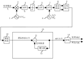
図1はこの発明の実施の形態1の構成を示すブロック図である。図において、15は本発明における固定周波数オフセットを持った第1局所発振器を、16は本発明におけるバンドパスフィルタを、17は加算器を、18は減算器11と積分器12と加算器17より主に構成されている改良AFC部を表し、それ以外の符号のものについては従来例と同一もしくは同一相当である。
【0012】
次に動作について説明する。図1において、周波数fcの受信電波と周波数fLO1+Δfの第1局所発振器15からの発振信号を、乗算器2に入力し、周波数fif−Δfを中心周波数とする中間周波数信号を作成する。ここでΔfは固定周波数オフセットを表し、fLO1+Δfで第1局所発振器の中心周波数の桁数を少なくさせるようにした周波数オフセットである。以下具体例として、ETC(Electronic Toll Collection System)用の通信装置等のDSRC(専用狭域通信)で利用される、受信電波の中心周波数fcを5840MHzとした場合の例について説明する。この際、伝送速度を2.048Mbaudとし、後段での復調処理のしやすさを考慮して、中間周波数信号の中心周波数を伝送速度の4倍である8.192MHzとする。
【0013】
このとき、従来例の装置では、第1局所発振器の周波数を5831.808MHzとして中間周波数信号を作成する必要がある。しかし、周波数の桁数が多いため、192kHzの固定周波数オフセットを持たせ、第1局所発振器の周波数を5832MHzとする。この例においては、192kHzがΔfに相当し、5832MHzがfLO+Δfに相当する。従って乗算器出力である中間周波数信号の中心周波数fif−Δfは8MHzとなる。乗算器出力は中心周波数がfif−Δfであるバンドパスフィルタ16により不要周波数成分を除去される。バンドパスフィルタ16の出力から遅延検波部10までの処理は従来例と同様である。遅延検波部10の出力を改良AFC部に入力させる。改良AFC部18は従来のAFC部13に固定周波数オフセットを補正させる機能を付加したものである。それは図1にもあるように積分器12と減算器11との間に加算器17を加え、積分器出力に固定周波数オフセットΔf分を加えたもので遅延検波出力を減算することにより固定周波数オフセットを含む周波数オフセットを補正するものである。図1では加算器に固定周波数オフセット分Δfを加えており、シンボルレートで動作することを想定している。固定周波数オフセットを含む周波数オフセットの補正後の減算結果をAFC出力とし、BTR部14に入力し、受信データと再生クロックを出力する。この改良AFC部18を用いることで、固定周波数オフセットを持った中間周波数信号でも復調を行うことが可能となる。
【0014】
実施の形態2.
図2はこの発明の実施の形態2の構成を示すブロック図である。図において、17は加算器、13は従来のAFC部を表し、それ以外は図1と同様である。
【0015】
次に動作について説明する。乗算器2から遅延検波10までの動作は実施の形態1と同様である。実施の形態2では遅延検波部10と従来のAFC部13との間に加算器17を挿入させる。遅延検波出力と固定周波数オフセットΔfを加算器17に入れることにより固定周波数オフセットΔfの補正を行う。なお、図2では加算器17の処理はシンボルレートで行っていることを想定している。固定周波数オフセットを補正された信号である加算器出力を従来のAFC部13に入力し、通常の周波数オフセット補正を行う。従来のAFC部13より出力されたAFC出力はBTR部14に入力され受信データと、それに同期した再生クロックを出力する。このように、従来のAFC部13の前に加算器17を挿入し固定周波数オフセットを補正させることにより、実施の形態1と同様の効果が得られ、また従来のAFC部をそのまま使用することが可能となる。
【0016】
実施の形態3.
実施の形態1、及び2においては復調装置にリミッタを用いているが、他の実施の形態として、図3、または図4のようにAGC(Automatic Gain Control :自動利得制御)を用いても構わない。また実施の形態1、及び2における構成以外でも、第1局所発振器で固定周波数オフセットを持たせ、実施の形態1のように固定周波数オフセット補正機能を付加した改良AFC部を用いる、または実施の形態2のように従来のAFC部の前段に加算器を付加させ固定周波数オフセットを補正させることで復調可能な構成ならば、別構成の復調装置でもよい。
【0017】
【発明の効果】
第1の発明によれば、従来よりも桁数の少ない周波数で発振する局所発振器を用いて中間周波数信号を復調させることが可能となる。
【0018】
第2の発明によれば、固定周波数オフセットを持った第1局所発振器と、乗算器と、不要周波数成分または高調波成分を除去するフィルタと、第2局所発振器と、AD変換器と、直交検波部と、位相検出部と、遅延検波部と、固定周波数オフセット分の補正を行うAFC部と、BTR部を備えることで、従来よりも桁数の少ない周波数で発振する局所発振器を用いて中間周波数信号を復調させることが可能となる。
【0019】
第3の発明によれば、固定周波数オフセットを持った第1局所発振器と、乗算器と、不要周波数成分または高調波成分を除去するフィルタと、第2局所発振器と、AD変換器と、直交検波部と、位相検出部と、遅延検波部と、固定周波数オフセット分の補正を行う加算器と、AFC部と、BTR部を備えることで、第1の発明と同様の効果が得られ、また従来のAFC部をそのまま用いることが可能となる。
【図面の簡単な説明】
【図1】 この発明の実施の形態1における復調装置の構成を示す図である。
【図2】 この発明の実施の形態2における復調装置の構成を示す図である。
【図3】 実施の形態1のリミッタをAGCに置き換えた他の形態の復調装置の構成を示す図である。
【図4】 実施の形態2のリミッタをAGCに置き換えた他の形態の復調装置の構成を示す図である。
【図5】 従来の復調装置の構成を示す図である。
【符号の説明】
1 従来例における第1局所発振器
2 乗算器
3 従来例におけるバンドパスフィルタ
4 リミッタ
5 ローパスフィルタ
6 第2局所発振器
7 AD変換器
8 直交検波部
9 位相検出部
10 遅延検波部
11 減算器
12 積分器
13 従来のAFC部
14 BTR部
15 本発明で用いる第1局所発振器
16 本発明で用いるバンドパスフィルタ
17 加算器
18 本発明における改良AFC部
19 AGC[0001]
BACKGROUND OF THE INVENTION
The present invention relates to a demodulator that demodulates a received signal by down-converting the received signal into an intermediate frequency signal based on an oscillation signal of a local oscillator.
[0002]
[Prior art]
Conventionally, in mobile communication, in order to demodulate received radio waves, demodulation processing is often performed by down-converting to an intermediate frequency using a local oscillator.
[0003]
QPSK modulation in a conventional: FIG. 5 shows a configuration example of (Quadrature Phase Shift K eying 4 value phase modulation) system demodulator. 1 is a first local oscillator in the conventional example, 2 is a multiplier, 3 is a bandpass filter that removes unnecessary frequency components of the multiplier output, 4 is a limiter, and 5 is a harmonic component of the limiter output. A low-pass filter, 6 a second local oscillator that samples the limiter output signal from which harmonic components have been removed, 7 an AD converter, 8 a quadrature detector for quadrature detection of the AD converter output, and 9 a
[0004]
Conventionally, as shown in FIG. 5, the received radio wave having the frequency fc and the first
[0005]
[Problems to be solved by the invention]
By the way, when the transmission rate is 2.048 Mbaud in the conventional example, since 2N times the transmission rate is selected as the center frequency of the intermediate frequency signal, the center frequency fif is 8.192 MHz, 12.292 MHz, or the like. Will be selected. Therefore, for example, when a carrier wave of 5840 MHz is used as a received radio wave, a first local oscillator having a center frequency of 5831.808 MHz must be employed when down-converting to an intermediate frequency signal.
[0006]
However, when the frequency of the first local oscillator becomes 5831.808 MHz or the like, the number of digits increases and a high-accuracy local oscillator is required. If the accuracy is not sufficiently satisfied, phase noise increases and reception performance deteriorates. there's a possibility that.
[0007]
Accordingly, an object of the present invention is to obtain a demodulator that creates an intermediate frequency signal using a local oscillator that does not require sufficient accuracy and demodulates a received signal.
[0008]
[Means for Solving the Problems]
A demodulating device according to a first aspect of the present invention includes a local oscillator that outputs an oscillation signal that is offset from the center frequency of a received radio wave, a multiplier that down-converts the received radio wave to an intermediate frequency signal based on the output of the local oscillator, and the multiplier An AD converter that converts the output signal into a digital signal, and a controller that performs a frequency offset correction for a fixed frequency on the output of the AD converter .
[0009]
A demodulator according to a second aspect of the present invention includes a first local oscillator that outputs an oscillation signal that is offset by a fixed frequency, and a multiplier that down-converts the received radio wave into an intermediate frequency signal based on the output of the first local oscillator. , A filter for removing unnecessary frequency components or harmonic components of the intermediate frequency signal output from the multiplier, a second local oscillator, and an output signal from which the harmonic components have been removed to the second local oscillator An AD converter for sampling based on the digital signal, a quadrature detection unit for quadrature detection of the output of the AD converter, a phase detection unit for detecting the phase of the quadrature detection output, and an output from the phase detection unit A delay detector that performs delay detection based on the phase detection data, and an offset corresponding to the fixed frequency is added to the integral value of the output of the delay detector, and the output of the delay detector From those having a AFC unit for performing frequency offset correction by subtracting the phase error of the added value, and a BTR section for outputting received data and the reproduction clock from the output signal of the AFC unit.
[0010]
A demodulating device according to a third aspect of the invention includes a first local oscillator that outputs an oscillation signal that is offset by a fixed frequency, and a multiplier that down-converts the received radio wave into an intermediate frequency signal based on the output of the first local oscillator. , A filter for removing unnecessary frequency components or harmonic components of the intermediate frequency signal output from the multiplier, a second local oscillator, and an output signal from which the harmonic components have been removed to the second local oscillator An AD converter for sampling based on the digital signal, a quadrature detection unit for quadrature detection of the output of the AD converter, a phase detection unit for detecting the phase of the quadrature detection output, and an output from the phase detection unit A delay detector that performs delay detection from the phase detection data, an adder that adds an offset of the fixed frequency to the output of the delay detector, and an output of the adder And AFC unit that performs subtraction to the frequency offset correcting the phase error of the integrated value of Luo said adders, in which a BTR section for outputting received data and the reproduction clock from the output signal of the AFC unit.
[0011]
DETAILED DESCRIPTION OF THE INVENTION
FIG. 1 is a block diagram showing the configuration of the first embodiment of the present invention. In the figure, 15 is a first local oscillator having a fixed frequency offset in the present invention, 16 is a bandpass filter in the present invention, 17 is an adder, 18 is a
[0012]
Next, the operation will be described. In FIG. 1, a received radio wave having a frequency fc and an oscillation signal from a first
[0013]
At this time, in the apparatus of the conventional example, it is necessary to create an intermediate frequency signal with the frequency of the first local oscillator set to 5831.808 MHz. However, since the number of digits of the frequency is large, a fixed frequency offset of 192 kHz is provided, and the frequency of the first local oscillator is 5832 MHz. In this example, 192 kHz corresponds to Δf, and 5832 MHz corresponds to fLO + Δf. Therefore, the center frequency fif-Δf of the intermediate frequency signal which is the multiplier output is 8 MHz. Unnecessary frequency components are removed from the multiplier output by a band-pass filter 16 whose center frequency is fif−Δf. The processing from the output of the bandpass filter 16 to the
[0014]
Embodiment 2. FIG.
FIG. 2 is a block diagram showing the configuration of the second embodiment of the present invention. In the figure, 17 represents an adder, 13 represents a conventional AFC unit, and the rest is the same as in FIG.
[0015]
Next, the operation will be described. The operations from the multiplier 2 to the
[0016]
Embodiment 3 FIG.
[0017]
【The invention's effect】
According to the first aspect of the invention, it is possible to demodulate the intermediate frequency signal using the local oscillator that oscillates at a frequency having a smaller number of digits than the conventional one.
[0018]
According to the second invention, a first local oscillator having a fixed frequency offset, a multiplier, a filter for removing unnecessary frequency components or harmonic components, a second local oscillator, an AD converter, and quadrature detection Unit, phase detection unit, delay detection unit, AFC unit for correcting a fixed frequency offset, and BTR unit, using a local oscillator that oscillates at a frequency with a smaller number of digits than conventional ones. The signal can be demodulated.
[0019]
According to the third invention, a first local oscillator having a fixed frequency offset, a multiplier, a filter for removing unnecessary frequency components or harmonic components, a second local oscillator, an AD converter, and quadrature detection The same effect as that of the first invention can be obtained by providing the unit, the phase detection unit, the delay detection unit, the adder for correcting the fixed frequency offset, the AFC unit, and the BTR unit. The AFC unit can be used as it is.
[Brief description of the drawings]
FIG. 1 is a diagram showing a configuration of a demodulator according to
FIG. 2 is a diagram showing a configuration of a demodulation device according to Embodiment 2 of the present invention.
FIG. 3 is a diagram illustrating a configuration of a demodulator according to another embodiment in which the limiter according to the first embodiment is replaced with AGC.
4 is a diagram illustrating a configuration of a demodulator according to another embodiment in which the limiter according to the second embodiment is replaced with AGC. FIG.
FIG. 5 is a diagram illustrating a configuration of a conventional demodulator.
[Explanation of symbols]
DESCRIPTION OF
Claims (3)
Priority Applications (1)
| Application Number | Priority Date | Filing Date | Title |
|---|---|---|---|
| JP2001306006A JP3818112B2 (en) | 2001-10-02 | 2001-10-02 | Demodulator |
Applications Claiming Priority (1)
| Application Number | Priority Date | Filing Date | Title |
|---|---|---|---|
| JP2001306006A JP3818112B2 (en) | 2001-10-02 | 2001-10-02 | Demodulator |
Publications (3)
| Publication Number | Publication Date |
|---|---|
| JP2003110641A JP2003110641A (en) | 2003-04-11 |
| JP2003110641A5 JP2003110641A5 (en) | 2005-06-09 |
| JP3818112B2 true JP3818112B2 (en) | 2006-09-06 |
Family
ID=19125711
Family Applications (1)
| Application Number | Title | Priority Date | Filing Date |
|---|---|---|---|
| JP2001306006A Expired - Lifetime JP3818112B2 (en) | 2001-10-02 | 2001-10-02 | Demodulator |
Country Status (1)
| Country | Link |
|---|---|
| JP (1) | JP3818112B2 (en) |
Families Citing this family (1)
| Publication number | Priority date | Publication date | Assignee | Title |
|---|---|---|---|---|
| JP4849037B2 (en) * | 2007-08-27 | 2011-12-28 | 岩崎通信機株式会社 | Automatic frequency control method and apparatus |
-
2001
- 2001-10-02 JP JP2001306006A patent/JP3818112B2/en not_active Expired - Lifetime
Also Published As
| Publication number | Publication date |
|---|---|
| JP2003110641A (en) | 2003-04-11 |
Similar Documents
| Publication | Publication Date | Title |
|---|---|---|
| JP4366808B2 (en) | Timing error detection circuit, demodulation circuit and method thereof | |
| JP3077881B2 (en) | Demodulation method and demodulation device | |
| US6731698B1 (en) | Quadrature demodulation circuit capable for canceling offset | |
| US20070047737A1 (en) | Fm stereo decoder incorporating costas loop pilot to stereo component phase correction | |
| CN100399774C (en) | Communication system and corresponding receiver | |
| JP3574679B2 (en) | Circuit arrangement for a demodulator of a wireless data signal in a broadcast receiver | |
| JP3818112B2 (en) | Demodulator | |
| JPH10163816A (en) | Automatic frequency control circuit | |
| JP4272997B2 (en) | Circuit for detecting an additional DC component contained in an input burst signal | |
| JP3979261B2 (en) | Receiver | |
| EP1060601A1 (en) | Demodulator having rotation means for frequency offset correction | |
| JP3876876B2 (en) | Radio receiver, detector circuit, radio clock, and repeater | |
| JPH0779363B2 (en) | Delay detection circuit | |
| JP4292667B2 (en) | Receiving apparatus and method thereof | |
| JP3094940B2 (en) | Quadrature modulated wave receiving method and apparatus | |
| WO2006046632A1 (en) | Digital wireless receiver | |
| WO2001008368A1 (en) | Apparatus for detecting frequency offset | |
| JP2001007875A (en) | Demodulation method and demodulation circuit in quadrature detection receiver | |
| JP4722673B2 (en) | FSK demodulation circuit | |
| JP2003110641A5 (en) | ||
| JP3366286B2 (en) | Digital receiver | |
| JP4637661B2 (en) | Modulation signal demodulator | |
| JP2001086175A (en) | VSB demodulator | |
| KR20040006661A (en) | Timing recovery Apparatus | |
| JPH0998198A (en) | Digital signal demodulator |
Legal Events
| Date | Code | Title | Description |
|---|---|---|---|
| RD01 | Notification of change of attorney |
Free format text: JAPANESE INTERMEDIATE CODE: A7421 Effective date: 20040706 |
|
| A521 | Written amendment |
Free format text: JAPANESE INTERMEDIATE CODE: A523 Effective date: 20040827 |
|
| A621 | Written request for application examination |
Free format text: JAPANESE INTERMEDIATE CODE: A621 Effective date: 20040827 |
|
| A977 | Report on retrieval |
Free format text: JAPANESE INTERMEDIATE CODE: A971007 Effective date: 20060517 |
|
| TRDD | Decision of grant or rejection written | ||
| A01 | Written decision to grant a patent or to grant a registration (utility model) |
Free format text: JAPANESE INTERMEDIATE CODE: A01 Effective date: 20060523 |
|
| A61 | First payment of annual fees (during grant procedure) |
Free format text: JAPANESE INTERMEDIATE CODE: A61 Effective date: 20060605 |
|
| R151 | Written notification of patent or utility model registration |
Ref document number: 3818112 Country of ref document: JP Free format text: JAPANESE INTERMEDIATE CODE: R151 |
|
| FPAY | Renewal fee payment (event date is renewal date of database) |
Free format text: PAYMENT UNTIL: 20100623 Year of fee payment: 4 |
|
| FPAY | Renewal fee payment (event date is renewal date of database) |
Free format text: PAYMENT UNTIL: 20100623 Year of fee payment: 4 |
|
| FPAY | Renewal fee payment (event date is renewal date of database) |
Free format text: PAYMENT UNTIL: 20110623 Year of fee payment: 5 |
|
| FPAY | Renewal fee payment (event date is renewal date of database) |
Free format text: PAYMENT UNTIL: 20120623 Year of fee payment: 6 |
|
| FPAY | Renewal fee payment (event date is renewal date of database) |
Free format text: PAYMENT UNTIL: 20130623 Year of fee payment: 7 |
|
| R250 | Receipt of annual fees |
Free format text: JAPANESE INTERMEDIATE CODE: R250 |
|
| R250 | Receipt of annual fees |
Free format text: JAPANESE INTERMEDIATE CODE: R250 |
|
| R250 | Receipt of annual fees |
Free format text: JAPANESE INTERMEDIATE CODE: R250 |
|
| R250 | Receipt of annual fees |
Free format text: JAPANESE INTERMEDIATE CODE: R250 |
|
| R250 | Receipt of annual fees |
Free format text: JAPANESE INTERMEDIATE CODE: R250 |
|
| R250 | Receipt of annual fees |
Free format text: JAPANESE INTERMEDIATE CODE: R250 |