JP3851679B2 - 空間光変調器 - Google Patents
空間光変調器 Download PDFInfo
- Publication number
- JP3851679B2 JP3851679B2 JP09704196A JP9704196A JP3851679B2 JP 3851679 B2 JP3851679 B2 JP 3851679B2 JP 09704196 A JP09704196 A JP 09704196A JP 9704196 A JP9704196 A JP 9704196A JP 3851679 B2 JP3851679 B2 JP 3851679B2
- Authority
- JP
- Japan
- Prior art keywords
- yoke
- address
- mirror
- pixel
- address electrode
- Prior art date
- Legal status (The legal status is an assumption and is not a legal conclusion. Google has not performed a legal analysis and makes no representation as to the accuracy of the status listed.)
- Expired - Fee Related
Links
- 239000000758 substrate Substances 0.000 claims description 31
- 239000010410 layer Substances 0.000 description 40
- 238000000034 method Methods 0.000 description 26
- 229910052751 metal Inorganic materials 0.000 description 15
- 239000002184 metal Substances 0.000 description 15
- 239000004065 semiconductor Substances 0.000 description 13
- 230000003287 optical effect Effects 0.000 description 10
- 229920002120 photoresistant polymer Polymers 0.000 description 9
- 238000012545 processing Methods 0.000 description 9
- 239000000463 material Substances 0.000 description 8
- 230000008569 process Effects 0.000 description 7
- 230000008901 benefit Effects 0.000 description 4
- 238000013461 design Methods 0.000 description 4
- 238000004519 manufacturing process Methods 0.000 description 4
- 125000006850 spacer group Chemical group 0.000 description 4
- 229910000838 Al alloy Inorganic materials 0.000 description 3
- XUIMIQQOPSSXEZ-UHFFFAOYSA-N Silicon Chemical compound [Si] XUIMIQQOPSSXEZ-UHFFFAOYSA-N 0.000 description 3
- 239000006096 absorbing agent Substances 0.000 description 3
- 239000000654 additive Substances 0.000 description 3
- 230000000996 additive effect Effects 0.000 description 3
- 230000015572 biosynthetic process Effects 0.000 description 3
- 230000000295 complement effect Effects 0.000 description 3
- 230000000873 masking effect Effects 0.000 description 3
- 229910052710 silicon Inorganic materials 0.000 description 3
- 239000010703 silicon Substances 0.000 description 3
- 101100277916 Caenorhabditis elegans dmd-10 gene Proteins 0.000 description 2
- 238000005411 Van der Waals force Methods 0.000 description 2
- 238000010586 diagram Methods 0.000 description 2
- 238000005516 engineering process Methods 0.000 description 2
- 230000006870 function Effects 0.000 description 2
- 230000014759 maintenance of location Effects 0.000 description 2
- 238000001465 metallisation Methods 0.000 description 2
- 238000012986 modification Methods 0.000 description 2
- 230000004048 modification Effects 0.000 description 2
- 230000003647 oxidation Effects 0.000 description 2
- 238000007254 oxidation reaction Methods 0.000 description 2
- 230000002829 reductive effect Effects 0.000 description 2
- 239000002356 single layer Substances 0.000 description 2
- RTAQQCXQSZGOHL-UHFFFAOYSA-N Titanium Chemical compound [Ti] RTAQQCXQSZGOHL-UHFFFAOYSA-N 0.000 description 1
- 229910052782 aluminium Inorganic materials 0.000 description 1
- XAGFODPZIPBFFR-UHFFFAOYSA-N aluminium Chemical compound [Al] XAGFODPZIPBFFR-UHFFFAOYSA-N 0.000 description 1
- 238000003491 array Methods 0.000 description 1
- 238000005513 bias potential Methods 0.000 description 1
- 230000005587 bubbling Effects 0.000 description 1
- 238000006243 chemical reaction Methods 0.000 description 1
- 239000011248 coating agent Substances 0.000 description 1
- 238000000576 coating method Methods 0.000 description 1
- 230000009977 dual effect Effects 0.000 description 1
- 230000000694 effects Effects 0.000 description 1
- 230000005611 electricity Effects 0.000 description 1
- 238000005530 etching Methods 0.000 description 1
- 230000001747 exhibiting effect Effects 0.000 description 1
- 230000010365 information processing Effects 0.000 description 1
- 230000002401 inhibitory effect Effects 0.000 description 1
- 239000004973 liquid crystal related substance Substances 0.000 description 1
- 238000005259 measurement Methods 0.000 description 1
- 150000002739 metals Chemical class 0.000 description 1
- 230000004297 night vision Effects 0.000 description 1
- 230000010287 polarization Effects 0.000 description 1
- 230000001681 protective effect Effects 0.000 description 1
- 230000009467 reduction Effects 0.000 description 1
- 238000012552 review Methods 0.000 description 1
- 230000035945 sensitivity Effects 0.000 description 1
- 230000003068 static effect Effects 0.000 description 1
- 238000012360 testing method Methods 0.000 description 1
- 239000010409 thin film Substances 0.000 description 1
- WFKWXMTUELFFGS-UHFFFAOYSA-N tungsten Chemical compound [W] WFKWXMTUELFFGS-UHFFFAOYSA-N 0.000 description 1
- 229910052721 tungsten Inorganic materials 0.000 description 1
- 239000010937 tungsten Substances 0.000 description 1
Images





Classifications
-
- G—PHYSICS
- G02—OPTICS
- G02B—OPTICAL ELEMENTS, SYSTEMS OR APPARATUS
- G02B26/00—Optical devices or arrangements for the control of light using movable or deformable optical elements
-
- G—PHYSICS
- G02—OPTICS
- G02B—OPTICAL ELEMENTS, SYSTEMS OR APPARATUS
- G02B26/00—Optical devices or arrangements for the control of light using movable or deformable optical elements
- G02B26/08—Optical devices or arrangements for the control of light using movable or deformable optical elements for controlling the direction of light
- G02B26/0816—Optical devices or arrangements for the control of light using movable or deformable optical elements for controlling the direction of light by means of one or more reflecting elements
- G02B26/0833—Optical devices or arrangements for the control of light using movable or deformable optical elements for controlling the direction of light by means of one or more reflecting elements the reflecting element being a micromechanical device, e.g. a MEMS mirror, DMD
- G02B26/0841—Optical devices or arrangements for the control of light using movable or deformable optical elements for controlling the direction of light by means of one or more reflecting elements the reflecting element being a micromechanical device, e.g. a MEMS mirror, DMD the reflecting element being moved or deformed by electrostatic means
Landscapes
- Physics & Mathematics (AREA)
- General Physics & Mathematics (AREA)
- Optics & Photonics (AREA)
- Mechanical Light Control Or Optical Switches (AREA)
- Transforming Electric Information Into Light Information (AREA)
Description
【産業上の利用分野】
本発明は一般的に、光学的光画像を形成する入射光を変調する光空間光変調器に関連し、更に詳細には、アドレス回路上に形成されるバイステイブル(bistable)・マイクロミラーのアレイを有するデジタル・マイクロミラー・デバイス(DMD)に関する。
【0002】
【従来の技術及びその課題】
空間光変調器(以下SLM)には、光学的な情報処理の分野において、投射ディスプレイ、ビデオ・モニター、グラフィック・モニター、テレビ及び電子写真プリントなど多数の用途がある。SLMは空間パターンの入射光を変調し、電気的又は光学的入力に対応する光画像を形成する装置である。入射光は、フェーズ、強度、偏光、又は方向において変調され得る。光変調は、電子光学的又は磁気光学的効果を示す種々の材料によって、又は表面変形による光を変調する材料によって達成される。
【0003】
SLMは典型的に、アドレス可能な画像素子(画素)の領域又は線形アレイから形成される。ソース画素データは、まず通常SLMの外にある関連する制御回路によってフォーマットされ、その後、1度に1フレームが画素アレイにロードされる。この画素データは、種々のアルゴリズム、つまり、トップからボトムへ順に1度に1画素ラインを、あるいは一つおきの画素ライン、例えば奇数列の画素を、トップからボトムへ順にアドレス指定し、その後偶数画素ラインへリターンすることによってインターリーブするなど、を用いて画素アレイに書込まれ得る。陰極線管(CRT)では、このデータ書込み技術は、高電力電子ガンが発光体の画素を左から右へ一度に横切ってスキャンするラスター化として周知である。この画素アドレス書込み方式は液晶ディスプレイ(LCD)にも応用することができる。
【0004】
テキサス州ダラスのテキサス・インスツルメンツの最近のイノベーションは、デジタル・マイクロミラー・デバイス又は変形ミラー・デバイス(総称してDMD)である。DMDはディスプレイ、プロジェクタ、及びハードコピープリンタの用途に適している電子的/機械的/光学的SLMである。DMDは、モノリシック単一チップ集積回路SLMであり、17ミクロンセンター上の16ミクロン四方の可動マイクロミラーの高密度アレイを有する。これらのミラーは、SRAMアレイセル及びアドレス電極を有するアドレス回路上に形成される。各ミラーはDMDアレイの1画素を形成し、バイステイブル、つまり2つの位置のうち1つの位置で安定(ステイブル)であり、ミラーアレイ上に向けられた光源は2方向のうち一方に反射される。1つの安定“オン”状態において、そのミラーへの入射光は投射レンズへ反射され、表示スクリーン又はプリンタのフォトセンシティブ素子にフォーカスされる。他方の“オフ”ミラー位置において、ミラーへ向けられる光は光アブソーバーに偏向される。アレイの各ミラーは、投射レンズ又は光アブソーバーのいずれかへ入射光を導くよう個別に制御される。投射レンズは、表示スクリーン上へ、画素ミラーから変調された光を最終的にフォーカスし拡大し、表示する場合の画像をつくる。DMDアレイの各画素ミラーが“オン”の位置である場合、表示される画像は明るい画素のアレイであり得る。
【0005】
DMDデバイス及びその利用についてのより詳細な説明は、本発明と同じ譲渡人に譲渡されている、Hornbeckの米国特許番号第5,061,049号、発明の名称『空間光変調器およびその方法』、DeMondらの米国特許番号第5,079,544号、発明の名称『標準独立デジタル化ビデオシステム』、及びNelsonの米国特許番号第5,105,369号、発明の名称『プリンティング・システム露光モジュール整合方法及び製造方法』を参照されたい。本発明と同じ譲渡人に譲渡され、参照のためここに引用する、米国特許番号第5,278,652号、発明の名称『パルス幅変調されたディスプレイ・システムを用いるためのDMDアーキテクチャ及びタイミング』に記載されたように、画像を形成する画素のグレイ・スケールは、ミラーのパルス幅変調技術によって達成される。
【0006】
DMDはそれが真にデジタル・ディスプレイ・デバイスであり、集積回路ソリューションである点で革新的である。DMDの進歩及び変化は、共に譲渡される種々の特許を参照することによって理解され得る。DMD空間光変調器の『第1世代』はミラーとビームが同一のものである可撓性ビームを実現した。つまり、電子静電力がミラーと下部アドレス電極との間に作られ、その撓みを誘導する。これらのミラーの撓みは可変であり、アナログモードで作動し、リーフ・スプリング又は片持ちばりビームで構成され得ることは、共に譲渡された、Hornbeckの米国特許番号第4,662,746号、発明の名称『空間光変調器およびその方法』、Hornbeckの米国特許番号第4,710,732号、発明の名称『空間光変調器およびその方法』、Hornbeckの米国特許番号第4,956,619号、発明の名称『空間光変調器』、Hornbeckの米国特許番号第5,172,262号、発明の名称『空間光変調器およびその方法』に開示されており、ここに参照のため引用する。
【0007】
この第1世代のDMDは、デジタル又はバイステイブル・デバイスとしても実施され得る。ビーム(ミラー)は、ねじれヒンジで支持され、ミラー片が着地パッド(landing pad )上に着地するまで、2方向のうち1方向に10度軸回転するミラーを有し得る。このような実施例は、共に譲渡されたHornbeckの米国特許番号第5,061,049号、発明の名称『空間光変調器およびその方法』に開示されている。ミラー片と着地パッドとの間のファン・デル・ワールスの力を制限するため、着地パッドは、着地パッド上に形成される配向(oriented)単分子層によって不活性化され得る。この単分子層は、ヴァン・デル・ワールの力を減少させ、ミラーが電極に膠着(stick )するのを防ぐ。この技術は、共に譲渡されたHornbeckの米国特許番号第5,331,454号、発明の名称『DMDのための低リセット電圧プロセス』に開示されており、参照のためここに引用する。
【0008】
DMDの『第2世代』は、共に譲渡された米国特許番号第5,083,857号、発明の名称『多レベル変形可能ミラー・デバイス』及び同時係属特許出願で1993年12月21日に出願された、出願番号第08/171,303、発明の名称『改良された多レベル・デジタル・マイクロミラー・デバイス』で実施されている。この第2世代のデバイスでは、ミラーはヨーク上に持ち上げられ、このヨークは一対のねじれヒンジによってアドレス回路上に懸架されている。この出願の図3cに示すように、電子静電力は、高架ミラー及び高架電極の間に生じる。回転するときに着地電極と接触するのはヨークであり、ミラー片は、どの構成物とも接触しない。ミラーの約50%である、ヨークのより短いモーメントのアームは、ミラー片が自由に動くために、リセットパルスによりエネルギーがより効果的にミラーに接続されるようにする。共振リセットパルスをミラーに提供することによって、ミラーが旋回(ピボット)構造を着地電極から自由にすることは、共に譲渡された米国特許番号第5,096,279号、発明の名称『空間光変調器およびその方法』、及び米国特許番号第5,233,456号、発明の名称『共振ミラーとその製造方法』に開示されている。しかし、ヨークがアドレス電極の表面領域をわずかに減少させるため、第1世代のデバイスに比べ、ミラーと高架アドレス電極との間に生じるアドレス・トルクが多少犠牲になる。
【0009】
より効率的なリセット動作を有する改良されたDMDを提供し、より多くのアドレス・トルク、ラッチ・トルク、及びアドレス保持トルクを有するデバイスを開発することが望まれている。改良されるデバイスは、基準の製造工程を用いることによって製造されることが好ましい。
【0010】
【課題を達成するための手段及び作用】
本発明は、ヨークが第1のアドレス電極対の実質的な部分を覆うように、ヒンジと平行にヨークを水平に伸ばすことによって、DMD空間光変調器としての技術的利点を達成する。第2の高架アドレス電極対が、ヨークの横およびヨークに支えられた高架ミラーの下に設けられる。アドレス・トルクは、第1のアドレス電極対とヨークの間、および第2の高架アドレス電極対と高架ミラーの間で達成される。ヨークは、ミラーが高架アドレス電極に関連して配置されるより下部アドレス電極により近接して配置される。対向部材間のユニット(単位)領域毎の力は距離の自乗分の一に比例するため、ヨークと下部の第1のアドレス電極対の間のユニット領域毎の力は、ミラーと第2の高架アドレス電極対の間のユニット領域毎の力より4倍の大きさまで大きくなる。本発明は、従来の世代に比べて、処理工程を変えることなく、高度なアドレス・トルク、ラッチ・トルク、アドレス保持トルク、及び復元力を有する。
【0011】
本発明は、基板を有する空間光変調器を構成する。第1の部分を有するアドレス回路は基板に近接して提供され、更に基板上に高架される第2の部分を有する。ヨークは、アドレス回路の第1の部分上に支持される。少なくとも1つのヒンジがヨークに接続され、ヨークを支持し、ヒンジはアドレス回路の第1の部分上のヨークを撓ませ得る。画素は、ヨークの上に持ち上げられ、ヨークに支持され、この画素は高架アドレスの第2部分の上に位置する。このアドレス回路の第1及び第2の部分は、互いに電気的に接続され、それによって第1及び第2の部分に提供される電位は、2平面に電子静電力を生じさせる。まず、電子静電力はヨークとアドレス回路の第1の部分の間に、次に、高架画素と高架第2の部分との間に生じる。
【0012】
ヨークと第1の部分との間の距離は、画素と高架第2の部分との間で定められる距離の約半分である。ヨークとアドレス回路の第1の部分の対向する表面領域は、高架画素と高架第2の部分との間に生じるアドレス・トルクより約4倍大きいアドレス・トルクを実現する。ネット・アドレス・トルクは付加的であり、前の世代のDMDデバイスによって生じるアドレス・トルクよりも実質的に大きい。
【0013】
ヨークは、ヨーク軸の両側に一対のヨーク片を有する、蝶のような形をしていることが好ましい。回転すると、一対のヨーク片の一方が着地パッドに着地し、それにより支持され、持ち上げられる画素ミラーは、どの構造物とも離れたままになる。このように、リセット・パルスは、ミラーに提供され得、良好なリセット動作を達成するため、ミラーに共振する周波数であることが好ましい。ヨークは、実質的にヒンジと同じ平面であることが好ましく、ヒンジが正確な整合及びバランスで形成されるように、単一エッチング工程を用いて形成され得る。
【0014】
空間光変調器は、アドレス回路に接続される制御回路を更に有する。この制御回路は、アドレス回路の第1及び第2の部分の両方にアドレスデータを提供し、画素を撓ませる。アドレス回路の第1の部分はパッドを有し、回転の画素軸の両側に提供され、離れているアドレス回路の第2の部分はこのヨーク軸の両側の画素の下に提供されることが好ましい。制御回路は、これらの一連のアドレス指定する部分のいずれか1つにアドレスデータを提供し、アドレス指定する部分の方へヨークとミラーを撓ませ、アドレス指定された第1及び第2の部分の方へヨークおよびミラーを撓ませる。画素はミラーであり、ヒンジに対して45度の角度でジオメトリックに配向されたの四角形であり、暗視界光学系(darkfield optics)によって感知される画素の端に沿って生じる回折項(diffraction terms )を最小化することが好ましい。
【0015】
一対のアドレス電極上に懸架されたヨークを有し、第2のアドレス電極対上に伸びる高架ミラーを支持するDMDデバイスは、アドレス電極と旋回構造物、つまり、ヨークとミラー、との間の引付ける(attractive)領域を大きく増加させる。アドレス基板上の下部アドレス電極は、金属3から構成され、アトラクティブ領域を最大にするよう注意深く設計され、ミラー及びヨークと同じ電位を有する着地電極上にヨーク片を着地させる。ミラーの高架アドレス電極は、第2世代のデバイスから修正されて本発明の延長ヨークを提供(accommodate )一方、ミラーと高架電極の間に生じ得るトルクのほとんどを維持する。高架電極の減少された領域の結果の損失トルクはアドレス・トルク上に伸びるヨークによって補償されるよりも多く、これらのアドレス電極は、高架電極に対し位置付けられるミラーよりヨークからその半分の距離に位置付けられる。第2世代のデバイスに比べて、生じるネット・アドレス・トルクは、約2倍(a factor of two )大きい。本発明は更に、より大きいラッチ・トルク及びアドレス保持トルクを達成する。
【0016】
【実施例】
本発明の一実施例を図面を参照して説明する。
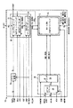
図1において、デジタル・マイクロミラー・デバイス(DMD)を有する空間光変調器を全体として10で示す。DMD10は、単一チップ集積回路であって、864×576マイクロミラー・アレイ12を有するように示されている。アレイ12は、864×36メモリセルアレイ16上にモノリシックに形成される。図2に示すように、メモリセルアレイ16を形成する36列のメモリセル(MR0−MR35)列の各メモリセルは、ある特定の16画素グループ(18)に関連され、制御する。各メモリセルは、一次の1ビット静電ランダムアクセスメモリ(SRAM)及びその一次セルによってフィードされる二次の1ビットSRAMセルを有する。メモリセルの各864列のそれぞれに接続される864ビットラインBL0−BL863がある。列画素データは、関連するビットラインBL0−BL863を介して、アドレス指定された一次メモリセル行MRn にロードされる。一次メモリセルは、それぞれWDn 又はRDn として識別される、関連する行の書込み可能又は読出し可能ラインをイネーブルにすることによってアドレス指定され、WPn は行MRn の各一次セルのイネーブル入力に接続される。この画素データは、グローバル制御ラインMXFRBをイネーブルにすることによってそれぞれ二次セルへ一次セルからラッチされ、MXFRBはアレイ16の全ての二次セルのイネーブル入力に接続されている。二次メモリセルは本質的にシャドウ・ラッチとして作動し、データは一次メモリセルから二次メモリセルへロードされ得、一次メモリセルが二次メモリセルのメモリセル内容に影響を及ぼすことなく新しい画素データを実質的に再ロードすることを可能にする。シャドウ・ラッチ技術の付加的説明は、共に譲渡された同時係属中の特許出願番号08/389,673で1995年2月16日に出願された、発明の名称『単一ビットライン・デュアル・ラッチ・メモリセルを有する空間光変調器』にされており、参照のためここに引用する。行アドレス及び列データロード回路、及びDMD10のテスト制御機能を有する制御回路の更に詳しい説明は、共に譲渡された同時係属中の特許出願番号08/373,692で1995年1月17日に出願された、発明の名称『モノリシック・プログラマブル・フォーマット・ピクセル・アレイ』にされており、参照のためここに引用する。
【0017】
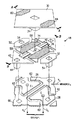
図2はミラーアレイ12の1つの画素18を示す。二次メモリセルのデータは、一対の相補性アドレス電極ラインに提供され、各ラインは順に、アレイ12の各画素18の下に形成され、画素に関連する2つのアドレス電極26及び28のうち1つに接続される。画素18は、支持ポスト34によって、全体として32で示すヨークの上に支持され、上に持ち上げられる四角形ミラー30を有する。支持ポスト34は、ミラーの中央から下方へ伸び、図示するように、そのねじれ軸にそってヨーク32の中央に取付けられ、ヨーク32上のミラー30の質量の中心のバランスをとる。ヨーク32は、通常は蝶の形であり、あとで詳細に説明するが、一対のねじれヒンジ40によって中央軸に沿って軸(axially )支持される。各ねじれヒンジ40の反対の端はそれぞれヒンジ支持ポスト44の頂点に定められているヒンジ支持ポストキャップ42に取付けられ、支持される。一対の高架ミラーアドレス電極50及び52は、それぞれアドレス支持ポスト54及び56によって支持される。
【0018】
アドレス支持ポスト54及び56、及びヒンジ支持ポスト44は、アドレス電極50及び52、ねじれヒンジ40、及びヨーク32をバイアス/リセット・バス60、及び一対の基板レベルアドレス電極パッド26及び28から離して上方に支持する。ミラー30及びヨーク32が共に、ヒンジ40により定められるヨークのねじれ軸の回りを回転するとき、ヨーク32の撓んだ側の一対のヨーク片58は着地サイト(site)62に着地し、バイアス/リセット・バス60とエンゲージ(engage)する。
【0019】
図3と共に図2を参照して、本発明の好ましい実施例に従った画素18の利点を詳細に説明する。ミラー30及びヨーク32の回転は、2方向のうち一方向になされ得、図5に示し後で説明するようなバイステイブル状態及びモジュール入射光を達成する。アドレス電圧が2つのアドレス電極パッド26又は28の一方に、及び関連する電極支持ポスト54及び56を介して、対応する高架ミラー・アドレス電極50又は52の一方に供給される。このアドレス電圧は、CMOSロジック回路と互換性のある5ボルトであり得るが、必要であれば他のレベルであっても良い。同時に、+15ボルトのバイアス電圧がバイアス/リセット・バス60に、支持ポスト44、ポストキャップ42、及びヒンジ40を介してヨーク32に、更に支持34を介してミラー30に供給される。本発明は、図2にハッチングされた領域で示す2つの場所で対向する表面間に電子静電力を供給する技術的利点を提供する。これらの電子静電引力は、図3の70、76、80、及び82にも示している。
【0020】
例示のため、図2及び図3に示されるように、ミラー30及びヨーク32が逆時計回りに回転される場合、0ボルト電位がアドレスラインVa上に供給され、相補性アドレスラインVa上に+5ボルトが供給される。その後、+15ボルト電位がバイアス/リセット・バス60へバイアスラインVb 上に供給され、ヨーク32及びミラー30上に+15ボルト電位を供給する。20ボルトの電位差から電子静電引力がアドレス電極26及びヨーク32のこの基板アドレス電極の上の部分の間に生じ、この力を全体として70で示す。アドレス電極26に懸かるヨーク32の対応する部分を、ハッチングされた部分74で示す。逆に、ミラーが時計回りに回転する場合、0ボルト電位が相補性アドレス電極28に供給され、76で引力が生じる。アドレス電極28に懸かるヨーク32の対応する部分をハッチングされた部分78で示す。
【0021】
ヨーク32の半分と下部アドレス電極26の間に電子静電引力が生じる一方、図3に80で示すような電子静電引力が高架アドレス電極50とミラー30の間にも生じる。この電子静電引力は、82で示す、高架アドレス電極50上に定められるミラー30の部分の間に作られる電圧電位によって生じる。アドレス電極52上に懸けられるミラー30の部分を84で示す。従って、1つのアドレス電極26又は28をアドレス指定することによって、対応する高架アドレス電極50又は52にアドレス電圧を順に供給し、電子静電力が70及び80又は76又は82で示す2つの場所で生じる。この0ボルトアドレス電位を2つのアドレス電極26又は28の一方に選択的に供給することにより、バイアス・バス60に、そして結果的にヨーク32及びミラー30に+15ボルト電位が供給されると、ミラー30及びヨーク32をどちらの方向に回転させるかが決定される。
【0022】
図3において、全体的にヨーク32と同平面であり、それぞれ約1ミクロンの距離でアドレス電極26及び28の上方に位置している高架アドレス電極50及び52を示す。高架アドレス電極50及び52と上のミラー30との距離は、この距離の約倍、つまり約2ミクロンである。対向する表面間の引力が対向する表面間の距離の二乗分の一の関数として直接変化するため、ヨーク32とアドレス電極26及び28の間に生じるユニット領域毎の電子静電引力は、ミラー30と対応する高架アドレス電極50及び52の間に生じる引力の大きさの4倍である。ねじれ軸の両側に生じる力は、付加的であり、共にミラー30とヨーク32をアドレス電極の方向へ回転させる。
【0023】
代替実施例において、高架電極50及び52、及び対応する支持ポストはなくてもよい。この実施例において、ヨーク32の上のミラー30の高さは、たったの約1ミクロンで、下部電極26及び28のディスタル・ローブ(distal lobe )により強い引力を達成する。撓むとき、ミラー30はアドレス電極26及び28の対応するディスタル・ローブへ向かって回転するが、まだエンゲージしない。この実施例では、ポスト44、ヨーク32及びミラー30を有する高架構造物は、すべて同じ電位であり、ショートの危険性が回避される。このように、1組の高架電極の限定は意図されない。
【0024】
アドレス・トルク(Ta )は、ヨーク32及びミラー30と共にアドレス電圧によって生じるトルクである。このアドレス・トルクは、同様のアドレス電圧及びバイアス電位の従来の世代のDMDデバイスで生じるアドレス・トルクよりずっと大きい。このように、本発明は、バイアス電圧が供給されるとき、ミラーが適切な方向に回転することを保証する必要のあるアドレス電圧Va と電位の間の差として定義される改良されたアドレスマージンを有する。
【0025】
本発明の画素は、ミラーを反対の状態へ回転(又はアップセット(upset ))させるに役立つアドレス電圧がある場合、バイアス電圧によって生じるラッチ・トルクの大きさとして定義される増加したラッチ・トルク(Tl )も有する。本発明の別の著しく改良された性能パラメータは、リセット後にバイアス電圧がオフの時間の間、その着地状態のミラーを保持するアドレス電圧の能力の大きさと定義されるアドレス保持トルク(Th )の増加である。本発明の別の改良された特徴は、単一パルスのリセットとヒンジの片によってつくられる復元力の組合せによって作られる片反応力の大きさと定義される復元力(Fr )の増加である。
【0026】
これらの4つすべての性能パラメータは、下部アドレス電極を有する電子静電力を生じさせるヨーク32を、高架ミラーと高架アドレス電極との間に生じる電子静電引力と共に用いる設計により、本発明によって実質的に前の世代のDMDデバイスより改良された。アドレス電極上の回転可能なヨークと実質的にその上の対向する表面領域との近接により、上述のすべての性能パラメータが著しく増加し、DMDデバイスの電子機械的効率を向上させる。特に、ヒンジの堅さ(stiffness )を変えることなく、前の世代のデバイスより1.8倍高いアドレス・トルクが達成される。ラッチ・トルクは、従来のDMDデバイスの2.6倍に改良される。生じる復元力は前の世代のDMDデバイスの8.8倍に増加される。すべての改良された性能パラメータにおいて、本発明の製造工程は、後に説明するが、前の世代のデバイスとほぼ同じであり、そのため前の世代のデバイスを超える“今までになかった”利点を提供する。
【0027】
本発明のDMDデバイスは、前述のように、空間光変調器の操作に重要な、より大きなマージン、アドレス・アップセットに対するより低い感知度、より低いリセット電圧要求、より高いスイッチスピードを含む。本発明の設計において、アドレス・マージン及びラッチ・マージンを改良するために必要であれば、より堅いヒンジの、非線形ヒンジを組込むこともできる。
【0028】
ファン・デル・ワールスの力による膠着の可能性を減らすため、着地電極60、特にヨーク32の片58からの接触点に対応する領域62、は不活性化され得る。着地電極を不活性化することにより、ヨーク32の付着又は膠着する傾向は減少され得る。膠着化は抑制力(inhibiting force)であり、ミラーをフラット状態にリセットするため、又はミラーを反対側に撓ませることのできるバイステイブル状態にスイッチするために供給される大きなリセット電圧を必要とする。着地電極を不活性化する方法は、共に譲渡されたHornbeckの米国特許番号第5,331,454、発明の名称『DMDの低リセット電圧処理』、及び共に譲渡された同時係属中の米国特許出願番号第08/239,497で1994年5月9日に出願された、発明の名称『マイクロ・メカニカル・デバイスのPFPEコーティング』に開示されており、参照のためここに引用する。ミラーのリセットを達成し、ミラーを別のバイステイブル状態の撓みに誘導するため、バイアス/リセット・ラインがミラーの共振周波数に対応する周波数の電圧、典型的に約5MHZ、でパルスされ得ることは、共に譲渡された米国特許番号第5,096,279、発明の名称『空間光変調器およびその方法』に開示されており、ここに参照のため引用する。
【0029】
図4はアレイ12の3×3アレイ部分の断面透視図であり、シリコン基板上の金属3層の形成を示し、この金属3層はアドレス電極及びシリコン基板上のバイアス/リセット・バスを定める。さらに高架ミラーアドレス電極、ポストキャップ、及び金属3層上のヨーク32を支持するヒンジも示す。ミラー支持ポストは、画素のねじれ軸にそって、それぞれのヨークによって支持されるように示されている。
【0030】
図5は光学的な略図であって、入射光は、ミラーが“オン”状態であるか“オフ”状態であるかによって、モジュレートされ2方向の一方に偏向されるように示されている。ミラー30がオン状態のとき、入射光は投射レンズを有する光学系に反射され、前面又は後面スクリーンプロジェクタの場合、結果的に表示スクリーンにフォーカスされ、電子写真プリンタの場合はフォトセンシティブ面上にフォーカスされる。ミラー30がオフ状態のとき、入射光は光アブソーバに反射され、暗視界光学系から離れる。ミラー30のバイステイブル状態の間の20度の回転は反射入射光の40度スウィングを成す。このように、本発明は、本発明の空間光変調器が意図した暗視界光学系システムで使用するのに重要な高コントラスト率の空間光画像を達成する。
【0031】
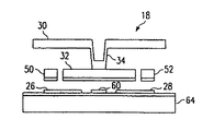
図6及び図7に関し、図2の線A−Aに沿ったピクセル18の断面図を示し、支持ポストは示されていない。図6に示すように、ヨーク32及びミラー30が非偏向(フラット)状態であり、ヨーク32は全体的に高架アドレス電極50及び52と同平面であり、アドレス電極26及び28、及びリセット/バイアス60を含む金属3層上に約1ミクロンの距離にある。ミラー30は一対の高架アドレス電極50及び52上に、基板64からヨークを離している距離の約2倍である、約2ミクロン上に持ち上げられる。
【0032】
図7において、図示するように、ヨーク32及びミラー30がアドレス指定され、時計方向に回転されるとき、ヨーク32のアドレス指定される半分の一対の着地片58はリセット/バイアス・バス60の部分62上に着地する。しかし、それと共に回転する高架ミラー30は上に位置したままであり、対応する高架アドレス電極52から離れている。図示するように、ヨーク32のモーメント・アームはねじれ軸のまわりのミラー30のモーメント・アームの約半分である。ミラー30と比較し着地ヨーク32の寸法がより短いとスタック・ミラーをリセットするために必要なトルクを減少するが、非常に短い着地ヨークを用いるとねじれヒンジ上に付加圧力を起こし得る。共に譲渡され、同時係属中の特許出願番号第08/171,303で1993年12月21日に出願された、発明の名称『マルチ・レベル・デジタル・マイクロミラー・デバイス』の記載を参照すれば上述のこれらの力をより良く理解できる。ヨーク32は一対の反対の片58上に着地し、対称的に設計されているため、アドレス電極26及び28の大きな領域は、図2に示すように、ヨーク32の下に定められ得る。更に、ヨークと着地電極の部分62の間の膠着力の減少がみられるため、ミラーの状態を変化又はリセットするときに供給されるより低いリセット電圧を必要とする。
【0033】
図8〜13を参照して、1画素18を形成するために行なわれる半導体形成工程の詳しい説明をする。測定を目的とするのではなく、説明及び明確化のため、各図面は図2の線B−Bに沿った断面図を示す。
【0034】
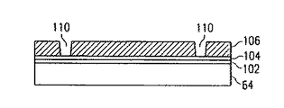
まず、図8 において、シリコン基板64はメモリセル16のアレイ、行アドレス回路20、及び列データロード回路30を含む下部アドレス回路を形成するよう処理される。その後、基板64は保護酸化物層102で覆われる。次に、通常M3と呼ばれる第3の金属化層が部分的に処理されたウェハ上にスパッタ・デポジットされ、104で表される。この第3の金属化層はパターニングされ、エッチングされ、図2に示すようなアドレス電極26及び28、及びバイアス/リセット・バス60を定める。次に、ヒンジ・スペーサ層106はアドレス回路上にスピン・デポジットされ、好ましくは1ミクロンの厚さを有するポジ型フォトレジストを有する。一対のバイア(via) 110がフォトレジスト層106を通って開けられ、ヒンジ支持ポストの形成を容易にし、フォトレジスト層106は後続の処理工程の間のフロー及びバブリング(bubbling)を避けるため高温でディープUV硬化する。
【0035】
図9において、金属化薄膜ヒンジ層112はフォトレジスト層106上及びバイア110にスパッタ・デポジットされる。ヒンジ層112は、約500 オングストロームの厚さを有することが好ましく、アルミニウム、アルミニウム合金、チタン化タングステン、及び本発明に適当な他の導電性金属から構成され得る。ヒンジ支持ポスト44は図示したようにこの工程で定義(define)され、バイアス/リセット・バス60に電気的に接続される。更にこの工程の間、一対の電極支持ポスト54及び56が定められ、図示していないが、フォトレジスト層106に形成される、対応する一対のバイア110に層112がスパッタ・デポジットされ、これらのバイアはバイア110が開けられる前述の工程の間に形成されている。このように、電極支持ポスト及びヒンジ支持ポストは非常に似ている。フォトレジスト層106の厚さはヒンジ・エアー・ギャップを決定し、そのため、それが着地電極とエンゲージするまでのヨーク32の角度自由度によりミラー回転角度が決定する。
【0036】
図10において、第1酸化マスクがプラズマ・デポジットされ、ヒンジ40の形にパターニングされる。その後、典型的に約3000オングストロームの厚さであるアルミニウム合金の厚い金属化層がデポジットされる。第2酸化マスクはプラズマ・デポジットされ、その後ヨーク32、高架電極54及び56、及びヒンジ支持キャップ42の形にパターニングされる。その後、薄いヒンジ層112及びより厚い金属層は、図示するようにアドレス電極50及び52、ヒンジ支持キャップ42及びヒンジ40を定めるようにエッチングされる。これらの構造を定めるために、単一プラズマ・エッチが用いられる。2つの酸化物層はエッチ・ストップとして機能し、それらの下の金属層を保護する。プラズマ・エッチ工程が終了した後、酸化物エッチ・ストップは、薄い金属ヒンジ、より厚い金属支持ポストキャップ42、電極50及び54から、及び図10に示すヒンジ40から除去される。
【0037】
図11において、厚いミラー・スペーサ層122はヒンジ、電極、及び支持キャップ上にスピン・デポジットされ、約2ミクロンの厚さを有するポジ型フォトレジストで構成されることが好ましい。バイア124がフォトレジスト・スペーサ層122に開けられ、図示するように、ヨーク32上の開口部を提供し、その後フォトレジスト層122はディープUV硬化される。
【0038】
図12において、その後アルミニウム合金で構成され反射性を有するミラー金属層は、約4000オングストロームの厚さにスパッタ・デポジットされる。この層はミラー支持ポスト34とミラー30の両方を形成する。その後マスキング酸化物層が、ミラー層上にプラズマ・デポジットされ、四角ミラーの形にパターニングされる。その後、図示するように、ミラー金属層はプラズマ・エッチングされ、ミラー30及び支持ポスト34を形成する。マスキング酸化物層は、ウェハがその後処理されダイを得るために切られる間、典型的にその場に残される。図13において、チップはプラズマ・エッチング・チェンバに配置され、そこではマスキング酸化物層と両方のスペーサ層106及び122がプラズマ・エッチングされて取除かれ、ヒンジ40とヨーク32の下にヒンジ・エアー・ギャップを、高架ミラー30下にミラー・エアー・ギャップ134を残す。
【0039】
図14は、本発明の代替実施例の分割した透視図を、全体として200で示す。画素200は図1〜13で示した画素18と非常に類似しており、同様の数字が同様の要素を表す。しかし、図示するように、画素200は、ねじれ軸の両側に1つの着地片204を有するように僅かに修正したヨーク202を有する。回転するとき、それが対応する着地電極208とエンゲージするか着地するまでヨーク202の一端204は回転する。ヨーク202は、基板上の金属3層から形成される一対のアドレスパッド210及び212のいずれかに実質的に重なる。電子静電力をつくる対向する表面の対応する領域はハッチングされた領域214、216、218及び220で示されている。ヒンジ222はヒンジポスト224からヨーク202を支持する。高架アドレス電極228及び230は、ヨーク202と同平面である。
【0040】
図15において、本発明の更に別の代替実施例を図300で示す。画素300は図(14の実施例示す)200、及び図1〜13に示す画素18に非常に類似しており、同様の数字は同様の要素を表す。図示するように画素300は、図14の実施例に類似する、ねじれ軸の両側に提供される1つの着地片も有する。図示するように、ヨーク302はねじれ軸に実質的に平行に下部アドレス電極の上に伸び、一対のアドレス電極304及び306はヨーク302の一方の下に提供され、別の対のアドレス電極310,312はXパターンを有するバイアス/リセット・バス320の別の側上に提供される。2つのアドレス電極304及び306は互いに電気的に結び付き、別の対のアドレス電極310及び312は、電気的に結び付いている。アドレス電極の対は、図示するように、対応する支持ポスト336を介して、高架ミラーアドレス電極330及び332に接続される。電子静電引力の領域は350、352、354、356、358及び360のハッチングされた領域で表す。ヒンジ362はポスト364からヨーク302を支持する。この実施例において、バイアス/リセット・バス620はX型を有し、図示するように、一対のアドレス電極を二股に分ける。X型を有するため、バイアス/リセット・バスは、容易にしかも簡単に基板上の金属3層の隣接する画素と相互接続ができる。これにより、共通バイアス/リセット・バスを有する複数の画素行を制御する望ましいレイアウトが達成され得、スプリット・リセット技術を促進することは、共に譲渡された米国特許出願番号第08/300,356号で1995年2月16日に出願された、発明の名称『空間光変調器のための画素制御回路』に開示されており、参照のためにここに開示する。ヨーク片の着地サイトは340で示すバイアス/リセット・バスに沿って提供される。
【0041】
要約すると、画素ミラーの撓みを誘導する、2つの位置で生じる電子静電力を有するDMD形式の空間光変調器が開示される。先ず、引力が、ヨークと下部基板アドレス電極との間に生じる。更に、電子静電力が高架ミラーと高架アドレス電極の間に生じる。これらの電子静電力は付加的であり、従来の世代のDMDデバイスを超える改良された性能パラメータを実現する。ミラーと高架アドレス電極との間のスペースの2分の1に等しい距離で、ヨークが基板アドレス電極上方に離されるため、ユニット領域毎の引力はミラーと高架アドレス電極との間に生じる力より4倍大きい。本発明の設計は、より高いアドレス・トルク、より高いラッチ・トルク、より高いリセット力、及びより大きなアドレスマージンを達成する。画素はアドレス・アップセットに対する感度が低く、より低いリセット電圧を必要とし、共振リセット及び複数リセットパルスの必要性を減らし得る。より高いスイッチスピードが達成され、前述の改良された性能パラメータにより、非線形及びより堅い(stiff )なヒンジが実現され得る。画素アレイは基準の工程から大きく逸脱することなく製造することができる。このように、従来の世代を超える本発明の空間光変調器によって達成することのできる改良された性能パラメータは、従来の世代を超える“今までになかった”設計である。
【0042】
本発明は特定の好ましい実施例を参照して説明されたが、本説明を参照すればこの技術の分野の習熟者にとって、種々の変形及び修正は明白である。したがって、添付の特許請求の範囲はあらゆるこれらの変形及び組合せを包含することを意図する。
【0043】
以上の説明に関して更に次の項を開示する。
(1) 空間光変調器であって、
基板と、
前記基板に近接して提供される第1の部分と、前記基板上に高架される第2の部分とを有するアドレス回路と、
前記アドレス回路の第1の部分上に支持されるヨークと、
前記ヨークに接続され、前記ヨークを支持する少なくとも1つのヒンジであって、前記ヒンジは前記ヨークを撓ませ、
前記ヨーク上に高架され、ヨークによって支持され、前記高架アドレス回路の第2の部分上に位置付けられる画素
とを含む空間光変調器。
(2) 第1項に記載の空間光変調器であって、ヨーク軸に沿って前記ヨークを軸支持する一対の前記ヒンジを有する空間光変調器。
(3) 第1項に記載の空間光変調器であって、前記ヨークは、前記画素及び前記ヨークに重なる前記画素の幅より狭い幅を有する空間光変調器。
(4) 第2項に記載の空間光変調器であって、前記ヨークは、前記ヨーク軸の両側に一対のヨーク片を有する空間光変調器。
(5) 第4項に記載の空間光変調器であって、前記ヨークは、蝶の形を有する空間光変調器。
(6) 第1項に記載の空間光変調器であって、第1のスペーシングは前記ヨークと前記アドレス回路の第1の部分との間に定められ、第2のスペーシングは前記画素と前記アドレス回路の第2の部分との間に定められ、前記第1のスペーシングは前記第2のスペーシングより狭い空間光変調器。
(7) 第1項に記載の空間光変調器であって、前記ヨークは実質的に前記アドレス回路の第2の部分と同じ平面である空間光変調器。
(8) 第2項に記載の空間光変調器であって、対向する表面領域の第1の対は前記ヨークと前記アドレス回路の第1の部分との間に定められ、対向する表面領域の第2の対は前記画素と前記アドレス回路の第2の部分との間に定められ、前記対向表面領域の第2の対が、前記ヨーク軸からの対向表面領域の前記第1の対より前記ヨーク軸からの距離より大きく、横方向へ定められる空間光変調器。
(9) 第1項に記載の空間光変調器であって、前記基板上に構成され、前記画素に電気的に接続されるバイアス/リセット・バスを更に有する空間光変調器。
(10) 第1項に記載の空間光変調器であって、前記ヒンジは、前記ヨークと実質的に同じ平面である空間光変調器。
(11) 第1項に記載の空間光変調器であって、前記アドレス回路に結合される制御回路を更に有し、前記制御回路は前記アドレス回路の第1の部分及び第2の部分にアドレスデータを供給し、前記画素を撓ませる空間光変調器。
(12) 第2項に記載の空間光変調器であって、前記アドレス回路に結合される制御回路を更に有し、前記制御回路は前記アドレス回路の第1の部分のひとつにアドレスデータを提供し、前記アドレス指定された第1の部分の方へ前記ヨークを撓ませる空間光変調器。
(13) 第1項に記載の空間光変調器であって、前記ヒンジに接続され前記ヒンジを支持する支持ポストを更に有する空間光変調器。
(14) 第1項に記載の空間光変調器であって、前記アドレス回路の第1の部分及び第2の部分は互いに電気的に接続される空間光変調器。
(15) 第1項に記載の空間光変調器であって、前記画素はミラーである空間光変調器。
(16) 第15項に記載の空間光変調器であって、前記ミラーは四角形である空間光変調器。
(17) 第16項に記載の空間光変調器であって、前記ミラーは前記ヒンジに対し45度でジオメトリックに配向される空間光変調器。
(18) 空間光変調器であって、
基板と、
前記基板に近接して提供される第1の部分と、前記第1の部分で定められる平面上にある第2の部分とを有するアドレス回路と、
前記アドレス回路の第1の部分上に支持されるヨークと、
前記ヨークに接続され、前記ヨークを支持する少なくとも1つのヒンジであって、前記ヒンジは前記ヨークを撓ませ、
前記ヨーク上に高架され、ヨークによって支持され、前記高架アドレス回路の第2の部分上に位置付けられる画素
とを含む空間光変調器。
(19) 増加した性能パラメータを有するDMD型の空間光変調器10である。画素ミラー30がヨーク32によって支持され、幾つかの構造体の間に電子静電引力70,76,80,82が生じる。まず、高架ミラー30と高架アドレス電極50,52の間、次に、ヨーク32と下部アドレス電極26,28の間に生じる。画素30は、従来の世代のデバイスに比べ、高アドレス・トルク、高ラッチ・トルク、高い復元力、及びより大きなマージンを達成する。基板アドレス電極26,28上のヨーク32の近接により、大きな引力が実現され、画素はアドレス・アップセットに感度が低く、より小さなリセット電圧を必要とし、スイッチスピードをより早める。
【図面の簡単な説明】
【図1】本発明の好ましい実施例に従った空間光変調器のブロック図であり、マイクロミラーを有する画素アレイを制御する列アドレス及びコラムデータロード回路を有する。
【図2】図2に示すアレイの1つのDMD画素の分解透視図であって、可撓性ヨーク上に形成された高架マイクロミラーを有し、ヨークは一対のヒンジによって順に支持され、ハッチングした領域は高架ミラーと高架アドレス電極の間の電子静電を引付ける(attraction)領域を図示し、ヨークと下部アドレス電極の間は基板上の金属3を有する。
【図3】ミラーと高架アドレス電極との間、及びヨークと下部アドレス電極との間の電子静電引力を示し、ヨーク及びミラーは、バイアス/リセット・バスに電気的に接続され、同じ電圧バイアスを有する。
【図4】図1に示すアレイの画素の3×3アレイの断面図であり、基板レベルアドレス電極及び基板レベルバイアス/リセットパターンを限定する金属3層を示すため、幾つかのヨーク、高架アドレス電極及びヒンジ支持ポストが取り除かれ、下部基板レベルアドレス電極の一部に重なる高架ヨークを示すため高架ミラーの幾つかが取り除かれて示されている。
【図5】図4に示す画素ミラーが2方向のうち一方に入射光を偏向させる2つのステイブル偏向状態を示す。
【図6】高架ミラー・アドレス電極及び基板アドレス電極上に支持されたヨークを示すためヒンジ軸に沿った図1のDMDアレイの1画素の断面図。
【図7】図6の様に断面図であり、共に上に支持され1ステイブル状態に回転されるヨーク及びミラーを有し、ヨーク片はそれぞれ1対の着地パッド上に着地し、高架ミラーは高架ミラー・アドレス電極に離れて近接して残る。
【図8】従来のロバスト(robust)半導体処理技術を用いて図2の画素を形成するために処理される半導体材料の種々の層を順次示す。
【図9】従来のロバスト(robust)半導体処理技術を用いて図2の画素を形成するために処理される半導体材料の種々の層を順次示す。
【図10】従来のロバスト(robust)半導体処理技術を用いて図2の画素を形成するために処理される半導体材料の種々の層を順次示す。
【図11】従来のロバスト(robust)半導体処理技術を用いて図2の画素を形成するために処理される半導体材料の種々の層を順次示す。
【図12】従来のロバスト(robust)半導体処理技術を用いて図2の画素を形成するために処理される半導体材料の種々の層を順次示す。
【図13】従来のロバスト(robust)半導体処理技術を用いて図2の画素を形成するために処理される半導体材料の種々の層を順次示す。
【図14】本発明の好ましい実施例の代替例の分割透視図であって、ヨークはねじれ軸の両側で定められる1つの着地片のみを有する。
【図15】本発明の好ましい実施例の別の代替例の分割透視図であって、ヨークはねじれ軸の両側に1つの着地片を有し、ヨークは下部基板アドレス電極上にねじれ軸に平行に伸びる。
【符号の説明】
10 DMD型空間光変調器
26,28 下部アドレス電極
30 画素ミラー
32 ヨーク
70,76,80,82 電子静電引力
50,52 高架アドレス電極
Claims (2)
- 空間変調器であって、
基板に配置された制御回路路と、
前記基板近傍に配置され、前記制御回路に接続された第1のアドレス電極と、
前記第1のアドレス電極の上方で、当該第1のアドレス電極と電気的に接続された第2のアドレス電極と、
前記第1のアドレス電極の上方に配置されたヨークと、
前記ヨークに電気的に接続された画素であって、前記ヨークに支持されて前記第2のアドレス電極上方に配置された画素と、および
前記ヨークに接続され、かつ当該ヨークを支持する少なくとも一つのヒンジと、を備え、当該ヒンジは、前記ヨークと前記第1のアドレス電極、および前記画素と前記第2のアドレス電極との間の静電力で、前記ヨークと前記画素を第1の方向へ撓み可能とし、前記静電力は前記制御回路からの信号に応答する、
ことを特徴とする空間変調器。 - 請求項1に記載の空間変調器であって、さらに、
前記基板近傍に配置された第3のアドレス電極であって、前記ヨークは前記第3のアドレス電極の上方に配置され、および
前記第3のアドレス電極上方に配置されて当該第3のアドレス電極に電気的に接続された第4のアドレス電極と、前記ヨークに支持された前記画素は当該第4のアドレス電極上方に配置され、
前記第3及び第4のアドレス電極は前記制御回路に電気的に接続され、
前記ヒンジは、前記ヨークと前記第3のアドレス電極との間および前記画素と前記第4のアドレス電極間との静電力で、前記ヨークと前記画素を第2の方向に撓み可能とし、前記静電力は前記制御回路からの信号に応答する、
ことを特徴とする空間変調器。
Applications Claiming Priority (2)
| Application Number | Priority Date | Filing Date | Title |
|---|---|---|---|
| US08/424,021 US5535047A (en) | 1995-04-18 | 1995-04-18 | Active yoke hidden hinge digital micromirror device |
| US424021 | 1995-04-18 |
Publications (2)
| Publication Number | Publication Date |
|---|---|
| JPH08334709A JPH08334709A (ja) | 1996-12-17 |
| JP3851679B2 true JP3851679B2 (ja) | 2006-11-29 |
Family
ID=23681129
Family Applications (1)
| Application Number | Title | Priority Date | Filing Date |
|---|---|---|---|
| JP09704196A Expired - Fee Related JP3851679B2 (ja) | 1995-04-18 | 1996-04-18 | 空間光変調器 |
Country Status (8)
| Country | Link |
|---|---|
| US (1) | US5535047A (ja) |
| EP (1) | EP0738910B1 (ja) |
| JP (1) | JP3851679B2 (ja) |
| KR (1) | KR100416679B1 (ja) |
| CN (1) | CN1160218A (ja) |
| CA (1) | CA2173637C (ja) |
| DE (1) | DE69634222T2 (ja) |
| TW (1) | TW295631B (ja) |
Families Citing this family (421)
| Publication number | Priority date | Publication date | Assignee | Title |
|---|---|---|---|---|
| US6674562B1 (en) | 1994-05-05 | 2004-01-06 | Iridigm Display Corporation | Interferometric modulation of radiation |
| US6426013B1 (en) | 1993-10-18 | 2002-07-30 | Xros, Inc. | Method for fabricating micromachined members coupled for relative rotation |
| US6467345B1 (en) | 1993-10-18 | 2002-10-22 | Xros, Inc. | Method of operating micromachined members coupled for relative rotation |
| US6044705A (en) * | 1993-10-18 | 2000-04-04 | Xros, Inc. | Micromachined members coupled for relative rotation by torsion bars |
| US7123216B1 (en) | 1994-05-05 | 2006-10-17 | Idc, Llc | Photonic MEMS and structures |
| US7460291B2 (en) | 1994-05-05 | 2008-12-02 | Idc, Llc | Separable modulator |
| US7297471B1 (en) | 2003-04-15 | 2007-11-20 | Idc, Llc | Method for manufacturing an array of interferometric modulators |
| US8014059B2 (en) | 1994-05-05 | 2011-09-06 | Qualcomm Mems Technologies, Inc. | System and method for charge control in a MEMS device |
| US6680792B2 (en) | 1994-05-05 | 2004-01-20 | Iridigm Display Corporation | Interferometric modulation of radiation |
| US7138984B1 (en) | 2001-06-05 | 2006-11-21 | Idc, Llc | Directly laminated touch sensitive screen |
| US7550794B2 (en) | 2002-09-20 | 2009-06-23 | Idc, Llc | Micromechanical systems device comprising a displaceable electrode and a charge-trapping layer |
| KR100213281B1 (ko) * | 1994-10-31 | 1999-08-02 | 전주범 | 광로조절장치 |
| US5650881A (en) * | 1994-11-02 | 1997-07-22 | Texas Instruments Incorporated | Support post architecture for micromechanical devices |
| US5703728A (en) * | 1994-11-02 | 1997-12-30 | Texas Instruments Incorporated | Support post architecture for micromechanical devices |
| US5671083A (en) * | 1995-02-02 | 1997-09-23 | Texas Instruments Incorporated | Spatial light modulator with buried passive charge storage cell array |
| US6969635B2 (en) * | 2000-12-07 | 2005-11-29 | Reflectivity, Inc. | Methods for depositing, releasing and packaging micro-electromechanical devices on wafer substrates |
| US5835256A (en) * | 1995-06-19 | 1998-11-10 | Reflectivity, Inc. | Reflective spatial light modulator with encapsulated micro-mechanical elements |
| US6046840A (en) * | 1995-06-19 | 2000-04-04 | Reflectivity, Inc. | Double substrate reflective spatial light modulator with self-limiting micro-mechanical elements |
| US5739941A (en) * | 1995-07-20 | 1998-04-14 | Texas Instruments Incorporated | Non-linear hinge for micro-mechanical device |
| US6172496B1 (en) | 1995-09-18 | 2001-01-09 | James P. Karins | Static event detection/protection device |
| JP3512963B2 (ja) * | 1995-12-15 | 2004-03-31 | テキサス インスツルメンツ インコーポレイテツド | マイクロメカニカルデバイス |
| US6686291B1 (en) | 1996-05-24 | 2004-02-03 | Texas Instruments Incorporated | Undercut process with isotropic plasma etching at package level |
| US5914805A (en) * | 1996-06-27 | 1999-06-22 | Xerox Corporation | Gyricon display with interstitially packed particles |
| US6055091A (en) * | 1996-06-27 | 2000-04-25 | Xerox Corporation | Twisting-cylinder display |
| US5825529A (en) * | 1996-06-27 | 1998-10-20 | Xerox Corporation | Gyricon display with no elastomer substrate |
| US5754332A (en) * | 1996-06-27 | 1998-05-19 | Xerox Corporation | Monolayer gyricon display |
| US5904790A (en) * | 1997-10-30 | 1999-05-18 | Xerox Corporation | Method of manufacturing a twisting cylinder display using multiple chromatic values |
| US5894367A (en) * | 1996-09-13 | 1999-04-13 | Xerox Corporation | Twisting cylinder display using multiple chromatic values |
| US5922268A (en) * | 1997-10-30 | 1999-07-13 | Xerox Corporation | Method of manufacturing a twisting cylinder display using multiple chromatic values |
| US5771116A (en) * | 1996-10-21 | 1998-06-23 | Texas Instruments Incorporated | Multiple bias level reset waveform for enhanced DMD control |
| US7471444B2 (en) | 1996-12-19 | 2008-12-30 | Idc, Llc | Interferometric modulation of radiation |
| US6028689A (en) * | 1997-01-24 | 2000-02-22 | The United States Of America As Represented By The Secretary Of The Air Force | Multi-motion micromirror |
| DE19710597C1 (de) * | 1997-03-14 | 1998-07-23 | Block Augenoptische Und Ophtha | Vorrichtung zur Erzeugung eines beleuchteten Bereiches mit hoher, lokal veränderbarer Energiedichte mit Hilfe eines Lasers und einer DMD |
| DE69806846T2 (de) * | 1997-05-08 | 2002-12-12 | Texas Instruments Inc., Dallas | Verbesserungen für räumliche Lichtmodulatoren |
| US5817569A (en) * | 1997-05-08 | 1998-10-06 | Texas Instruments Incorporated | Method of reducing wafer particles after partial saw |
| US5903383A (en) * | 1997-05-19 | 1999-05-11 | The Charles Stark Draper Laboratory Inc. | Electrostatic memory micromirror display system |
| US5808780A (en) * | 1997-06-09 | 1998-09-15 | Texas Instruments Incorporated | Non-contacting micromechanical optical switch |
| US5790297A (en) | 1997-06-26 | 1998-08-04 | Xerox Corporation | Optical row displacement for a fault tolerant projective display |
| US5774254A (en) * | 1997-06-26 | 1998-06-30 | Xerox Corporation | Fault tolerant light modulator display system |
| DE19733370C2 (de) * | 1997-08-01 | 2000-07-06 | Agfa Gevaert Ag | Vorrichtung und Verfahren zum Kopieren von Bilder auf lichtempfindliches Aufzeichnungsmaterial |
| US5867302A (en) * | 1997-08-07 | 1999-02-02 | Sandia Corporation | Bistable microelectromechanical actuator |
| DE19757197A1 (de) * | 1997-12-22 | 1999-06-24 | Bosch Gmbh Robert | Herstellungsverfahren für mikromechanische Vorrichtung |
| US5900192A (en) * | 1998-01-09 | 1999-05-04 | Xerox Corporation | Method and apparatus for fabricating very small two-color balls for a twisting ball display |
| US5976428A (en) * | 1998-01-09 | 1999-11-02 | Xerox Corporation | Method and apparatus for controlling formation of two-color balls for a twisting ball display |
| US20040035690A1 (en) * | 1998-02-11 | 2004-02-26 | The Regents Of The University Of Michigan | Method and apparatus for chemical and biochemical reactions using photo-generated reagents |
| WO1999041007A2 (en) * | 1998-02-11 | 1999-08-19 | University Of Houston | Method and apparatus for chemical and biochemical reactions using photo-generated reagents |
| US6375903B1 (en) | 1998-02-23 | 2002-04-23 | Wisconsin Alumni Research Foundation | Method and apparatus for synthesis of arrays of DNA probes |
| US6206290B1 (en) | 1998-03-06 | 2001-03-27 | Symbol Technologies, Inc. | Control system for oscillating optical element in scanners |
| US7532377B2 (en) | 1998-04-08 | 2009-05-12 | Idc, Llc | Movable micro-electromechanical device |
| WO1999052006A2 (en) | 1998-04-08 | 1999-10-14 | Etalon, Inc. | Interferometric modulation of radiation |
| US8928967B2 (en) | 1998-04-08 | 2015-01-06 | Qualcomm Mems Technologies, Inc. | Method and device for modulating light |
| US6271957B1 (en) * | 1998-05-29 | 2001-08-07 | Affymetrix, Inc. | Methods involving direct write optical lithography |
| DE19824709A1 (de) * | 1998-06-03 | 1999-12-09 | Bundesdruckerei Gmbh | Erzeugung von Leuchtdichte-Arrays mit digitalem Array-Strahlungsprozessoren |
| US6962419B2 (en) | 1998-09-24 | 2005-11-08 | Reflectivity, Inc | Micromirror elements, package for the micromirror elements, and projection system therefor |
| US6529310B1 (en) | 1998-09-24 | 2003-03-04 | Reflectivity, Inc. | Deflectable spatial light modulator having superimposed hinge and deflectable element |
| US5991066A (en) * | 1998-10-15 | 1999-11-23 | Memsolutions, Inc. | Membrane-actuated charge controlled mirror |
| US6031657A (en) * | 1998-10-15 | 2000-02-29 | Memsolutions, Inc. | Membrane-actuated charge controlled mirror (CCM) projection display |
| US6123985A (en) * | 1998-10-28 | 2000-09-26 | Solus Micro Technologies, Inc. | Method of fabricating a membrane-actuated charge controlled mirror (CCM) |
| US6700606B1 (en) * | 1999-06-09 | 2004-03-02 | Activcard Ireland Limited | Micromirror optical imager |
| US6671005B1 (en) | 1999-06-21 | 2003-12-30 | Altman Stage Lighting Company | Digital micromirror stage lighting system |
| US7306338B2 (en) | 1999-07-28 | 2007-12-11 | Moxtek, Inc | Image projection system with a polarizing beam splitter |
| WO2003007049A1 (en) | 1999-10-05 | 2003-01-23 | Iridigm Display Corporation | Photonic mems and structures |
| US6396619B1 (en) | 2000-01-28 | 2002-05-28 | Reflectivity, Inc. | Deflectable spatial light modulator having stopping mechanisms |
| US6741383B2 (en) | 2000-08-11 | 2004-05-25 | Reflectivity, Inc. | Deflectable micromirrors with stopping mechanisms |
| US6529311B1 (en) * | 1999-10-28 | 2003-03-04 | The Trustees Of Boston University | MEMS-based spatial-light modulator with integrated electronics |
| US6412972B1 (en) | 1999-12-10 | 2002-07-02 | Altman Stage Lighting Company | Digital light protection apparatus with digital micromirror device and rotatable housing |
| US6440252B1 (en) | 1999-12-17 | 2002-08-27 | Xerox Corporation | Method for rotatable element assembly |
| US6466358B2 (en) * | 1999-12-30 | 2002-10-15 | Texas Instruments Incorporated | Analog pulse width modulation cell for digital micromechanical device |
| US6545671B1 (en) | 2000-03-02 | 2003-04-08 | Xerox Corporation | Rotating element sheet material with reversible highlighting |
| US6498674B1 (en) | 2000-04-14 | 2002-12-24 | Xerox Corporation | Rotating element sheet material with generalized containment structure |
| FR2807844B1 (fr) * | 2000-04-17 | 2003-05-16 | Commissariat Energie Atomique | Commutateur optique a pieces mobiles et son procede de realisation, et dispositif de brassage optique utilisant le commutateur optique |
| KR100708077B1 (ko) * | 2000-05-01 | 2007-04-16 | 삼성전자주식회사 | 화상표시장치용 마이크로미러 디바이스 |
| US6504525B1 (en) | 2000-05-03 | 2003-01-07 | Xerox Corporation | Rotating element sheet material with microstructured substrate and method of use |
| US6813053B1 (en) * | 2000-05-19 | 2004-11-02 | The Regents Of The University Of California | Apparatus and method for controlled cantilever motion through torsional beams and a counterweight |
| US6781742B2 (en) * | 2000-07-11 | 2004-08-24 | Semiconductor Energy Laboratory Co., Ltd. | Digital micromirror device and method of driving digital micromirror device |
| US7099065B2 (en) * | 2000-08-03 | 2006-08-29 | Reflectivity, Inc. | Micromirrors with OFF-angle electrodes and stops |
| US6545758B1 (en) * | 2000-08-17 | 2003-04-08 | Perry Sandstrom | Microarray detector and synthesizer |
| US6567163B1 (en) | 2000-08-17 | 2003-05-20 | Able Signal Company Llc | Microarray detector and synthesizer |
| US6847347B1 (en) | 2000-08-17 | 2005-01-25 | Xerox Corporation | Electromagnetophoretic display system and method |
| US7300162B2 (en) * | 2000-08-30 | 2007-11-27 | Texas Instruments Incorporated | Projection display |
| US6522454B2 (en) | 2000-09-29 | 2003-02-18 | Texas Instruments Incorporated | Hidden hinge digital micromirror device with improved manufacturing yield and improved contrast ratio |
| US6962771B1 (en) * | 2000-10-13 | 2005-11-08 | Taiwan Semiconductor Manufacturing Company, Ltd. | Dual damascene process |
| US20040080484A1 (en) * | 2000-11-22 | 2004-04-29 | Amichai Heines | Display devices manufactured utilizing mems technology |
| US6614576B2 (en) * | 2000-12-15 | 2003-09-02 | Texas Instruments Incorporated | Surface micro-planarization for enhanced optical efficiency and pixel performance in SLM devices |
| US6524500B2 (en) | 2000-12-28 | 2003-02-25 | Xerox Corporation | Method for making microencapsulated gyricon beads |
| US6897848B2 (en) | 2001-01-11 | 2005-05-24 | Xerox Corporation | Rotating element sheet material and stylus with gradient field addressing |
| US6690350B2 (en) | 2001-01-11 | 2004-02-10 | Xerox Corporation | Rotating element sheet material with dual vector field addressing |
| US6970154B2 (en) | 2001-01-11 | 2005-11-29 | Jpmorgan Chase Bank | Fringe-field filter for addressable displays |
| US6480320B2 (en) * | 2001-02-07 | 2002-11-12 | Transparent Optical, Inc. | Microelectromechanical mirror and mirror array |
| US6585378B2 (en) | 2001-03-20 | 2003-07-01 | Eastman Kodak Company | Digital cinema projector |
| US6589625B1 (en) | 2001-08-01 | 2003-07-08 | Iridigm Display Corporation | Hermetic seal and method to create the same |
| US7023606B2 (en) * | 2001-08-03 | 2006-04-04 | Reflectivity, Inc | Micromirror array for projection TV |
| JP3750574B2 (ja) * | 2001-08-16 | 2006-03-01 | 株式会社デンソー | 薄膜電磁石およびこれを用いたスイッチング素子 |
| KR100398310B1 (ko) | 2001-09-13 | 2003-09-19 | 한국과학기술원 | 엇물린 외팔보들을 이용한 마이크로미러 디바이스 및 그응용소자 |
| US6844952B2 (en) * | 2001-09-18 | 2005-01-18 | Vitesse Semiconductor Corporation | Actuator-controlled mirror with Z-stop mechanism |
| US6809851B1 (en) | 2001-10-24 | 2004-10-26 | Decicon, Inc. | MEMS driver |
| US6699570B2 (en) | 2001-11-06 | 2004-03-02 | Xerox Corporation | Colored cyber toner using multicolored gyricon spheres |
| US6885492B2 (en) | 2001-11-08 | 2005-04-26 | Imaginative Optics, Inc. | Spatial light modulator apparatus |
| EP1315016B1 (en) * | 2001-11-21 | 2006-08-23 | Texas Instruments Incorporated | Yokeless hidden hinge digital micromirror device |
| WO2003048836A2 (en) * | 2001-12-03 | 2003-06-12 | Flixel Ltd. | Display devices |
| US7116459B2 (en) * | 2001-12-27 | 2006-10-03 | Texas Instruments Incorporated | Field diode detection of excess light conditions for spatial light modulator |
| US7061561B2 (en) * | 2002-01-07 | 2006-06-13 | Moxtek, Inc. | System for creating a patterned polarization compensator |
| US6909473B2 (en) * | 2002-01-07 | 2005-06-21 | Eastman Kodak Company | Display apparatus and method |
| US6808269B2 (en) * | 2002-01-16 | 2004-10-26 | Eastman Kodak Company | Projection apparatus using spatial light modulator |
| US6794119B2 (en) | 2002-02-12 | 2004-09-21 | Iridigm Display Corporation | Method for fabricating a structure for a microelectromechanical systems (MEMS) device |
| US6574033B1 (en) | 2002-02-27 | 2003-06-03 | Iridigm Display Corporation | Microelectromechanical systems device and method for fabricating same |
| US20030187330A1 (en) * | 2002-03-28 | 2003-10-02 | Fuji Photo Optical Co., Ltd. | Electronic endoscope apparatus using micromirror device |
| US7018268B2 (en) * | 2002-04-09 | 2006-03-28 | Strasbaugh | Protection of work piece during surface processing |
| WO2003086955A1 (en) * | 2002-04-12 | 2003-10-23 | Fraunhofer-Gesellschaft zur Förderung der angewandten Forschung e.V. | Method and device for operating a micromechanical element |
| US6996292B1 (en) | 2002-04-18 | 2006-02-07 | Sandia Corporation | Staring 2-D hadamard transform spectral imager |
| US6676260B2 (en) | 2002-04-25 | 2004-01-13 | Eastman Kodak Company | Projection apparatus using spatial light modulator with relay lens and dichroic combiner |
| US6648475B1 (en) | 2002-05-20 | 2003-11-18 | Eastman Kodak Company | Method and apparatus for increasing color gamut of a display |
| US20040004753A1 (en) * | 2002-06-19 | 2004-01-08 | Pan Shaoher X. | Architecture of a reflective spatial light modulator |
| US20030234994A1 (en) * | 2002-06-19 | 2003-12-25 | Pan Shaoher X. | Reflective spatial light modulator |
| US20040069742A1 (en) * | 2002-06-19 | 2004-04-15 | Pan Shaoher X. | Fabrication of a reflective spatial light modulator |
| US7206110B2 (en) * | 2002-06-19 | 2007-04-17 | Miradia Inc. | Memory cell dual protection |
| US7034984B2 (en) | 2002-06-19 | 2006-04-25 | Miradia Inc. | Fabrication of a high fill ratio reflective spatial light modulator with hidden hinge |
| US6992810B2 (en) * | 2002-06-19 | 2006-01-31 | Miradia Inc. | High fill ratio reflective spatial light modulator with hidden hinge |
| US6736514B2 (en) | 2002-06-21 | 2004-05-18 | Eastman Kodak Company | Imaging apparatus for increased color gamut using dual spatial light modulators |
| US6843574B2 (en) * | 2002-08-20 | 2005-01-18 | Intel Corporation | Gimbaled micromechanical rotation system |
| JP2004101826A (ja) * | 2002-09-09 | 2004-04-02 | Fuji Photo Optical Co Ltd | プロジェクタ用光学系およびこれを用いたプロジェクタ装置 |
| US6809873B2 (en) * | 2002-09-09 | 2004-10-26 | Eastman Kodak Company | Color illumination system for spatial light modulators using multiple double telecentric relays |
| US7781850B2 (en) | 2002-09-20 | 2010-08-24 | Qualcomm Mems Technologies, Inc. | Controlling electromechanical behavior of structures within a microelectromechanical systems device |
| US6733144B2 (en) * | 2002-09-27 | 2004-05-11 | Intel Corporation | Shock protectors for micro-mechanical systems |
| US6870659B2 (en) * | 2002-10-11 | 2005-03-22 | Exajoule, Llc | Micromirror systems with side-supported mirrors and concealed flexure members |
| US6798560B2 (en) * | 2002-10-11 | 2004-09-28 | Exajoula, Llc | Micromirror systems with open support structures |
| US6769772B2 (en) * | 2002-10-11 | 2004-08-03 | Eastman Kodak Company | Six color display apparatus having increased color gamut |
| US6825968B2 (en) * | 2002-10-11 | 2004-11-30 | Exajoule, Llc | Micromirror systems with electrodes configured for sequential mirror attraction |
| US6802613B2 (en) * | 2002-10-16 | 2004-10-12 | Eastman Kodak Company | Broad gamut color display apparatus using an electromechanical grating device |
| US6807010B2 (en) * | 2002-11-13 | 2004-10-19 | Eastman Kodak Company | Projection display apparatus having both incoherent and laser light sources |
| US6947459B2 (en) * | 2002-11-25 | 2005-09-20 | Eastman Kodak Company | Organic vertical cavity laser and imaging system |
| US7405860B2 (en) * | 2002-11-26 | 2008-07-29 | Texas Instruments Incorporated | Spatial light modulators with light blocking/absorbing areas |
| TW200413810A (en) | 2003-01-29 | 2004-08-01 | Prime View Int Co Ltd | Light interference display panel and its manufacturing method |
| US20040150794A1 (en) * | 2003-01-30 | 2004-08-05 | Eastman Kodak Company | Projector with camcorder defeat |
| FR2850762A1 (fr) * | 2003-01-31 | 2004-08-06 | Commissariat Energie Atomique | Dispositif d'orientation d'un objet |
| US7042622B2 (en) * | 2003-10-30 | 2006-05-09 | Reflectivity, Inc | Micromirror and post arrangements on substrates |
| US6885494B2 (en) * | 2003-02-12 | 2005-04-26 | Reflectivity, Inc. | High angle micro-mirrors and processes |
| US7436573B2 (en) * | 2003-02-12 | 2008-10-14 | Texas Instruments Incorporated | Electrical connections in microelectromechanical devices |
| WO2004074167A2 (en) * | 2003-02-20 | 2004-09-02 | Technion Research & Development Foundation Ltd. | A device and method for stacked multi-level uncoupled electrostatic actuators |
| US6906848B2 (en) * | 2003-02-24 | 2005-06-14 | Exajoule, Llc | Micromirror systems with concealed multi-piece hinge structures |
| US6900922B2 (en) * | 2003-02-24 | 2005-05-31 | Exajoule, Llc | Multi-tilt micromirror systems with concealed hinge structures |
| US6758565B1 (en) | 2003-03-20 | 2004-07-06 | Eastman Kodak Company | Projection apparatus using telecentric optics |
| US6914711B2 (en) * | 2003-03-22 | 2005-07-05 | Active Optical Networks, Inc. | Spatial light modulator with hidden comb actuator |
| US7015885B2 (en) * | 2003-03-22 | 2006-03-21 | Active Optical Networks, Inc. | MEMS devices monolithically integrated with drive and control circuitry |
| US7375874B1 (en) | 2003-03-22 | 2008-05-20 | Active Optical Mems Inc. | Light modulator with integrated drive and control circuitry |
| US7221759B2 (en) * | 2003-03-27 | 2007-05-22 | Eastman Kodak Company | Projector with enhanced security camcorder defeat |
| TW594360B (en) | 2003-04-21 | 2004-06-21 | Prime View Int Corp Ltd | A method for fabricating an interference display cell |
| US7095546B2 (en) * | 2003-04-24 | 2006-08-22 | Metconnex Canada Inc. | Micro-electro-mechanical-system two dimensional mirror with articulated suspension structures for high fill factor arrays |
| TW570896B (en) | 2003-05-26 | 2004-01-11 | Prime View Int Co Ltd | A method for fabricating an interference display cell |
| EP1636628A4 (en) * | 2003-06-02 | 2009-04-15 | Miradia Inc | REFLECTIVE ROOM LIGHT MODULATOR WITH HIGH FILLING RATIO WITH HORIZONTAL SWITCHING MEMBER |
| US7221495B2 (en) | 2003-06-24 | 2007-05-22 | Idc Llc | Thin film precursor stack for MEMS manufacturing |
| US6839181B1 (en) * | 2003-06-25 | 2005-01-04 | Eastman Kodak Company | Display apparatus |
| US7212359B2 (en) * | 2003-07-25 | 2007-05-01 | Texas Instruments Incorporated | Color rendering of illumination light in display systems |
| US7131762B2 (en) * | 2003-07-25 | 2006-11-07 | Texas Instruments Incorporated | Color rendering of illumination light in display systems |
| US20050094241A1 (en) * | 2003-11-01 | 2005-05-05 | Fusao Ishii | Electromechanical micromirror devices and methods of manufacturing the same |
| TWI231865B (en) | 2003-08-26 | 2005-05-01 | Prime View Int Co Ltd | An interference display cell and fabrication method thereof |
| JP4406549B2 (ja) | 2003-09-22 | 2010-01-27 | 富士フイルム株式会社 | 光変調素子及び光変調アレイ素子並びにそれを用いた露光装置 |
| TW593126B (en) | 2003-09-30 | 2004-06-21 | Prime View Int Co Ltd | A structure of a micro electro mechanical system and manufacturing the same |
| JP2005121906A (ja) | 2003-10-16 | 2005-05-12 | Fuji Photo Film Co Ltd | 反射型光変調アレイ素子及び露光装置 |
| US8238019B2 (en) * | 2003-11-01 | 2012-08-07 | Silicon Quest Kabushiki-Kaisha | Projection apparatus with coherent light source |
| US7012726B1 (en) | 2003-11-03 | 2006-03-14 | Idc, Llc | MEMS devices with unreleased thin film components |
| US7026695B2 (en) * | 2003-11-19 | 2006-04-11 | Miradia Inc. | Method and apparatus to reduce parasitic forces in electro-mechanical systems |
| US7428353B1 (en) | 2003-12-02 | 2008-09-23 | Adriatic Research Institute | MEMS device control with filtered voltage signal shaping |
| US7295726B1 (en) | 2003-12-02 | 2007-11-13 | Adriatic Research Institute | Gimbal-less micro-electro-mechanical-system tip-tilt and tip-tilt-piston actuators and a method for forming the same |
| US7142346B2 (en) | 2003-12-09 | 2006-11-28 | Idc, Llc | System and method for addressing a MEMS display |
| US7161728B2 (en) | 2003-12-09 | 2007-01-09 | Idc, Llc | Area array modulation and lead reduction in interferometric modulators |
| US6902277B1 (en) | 2004-01-06 | 2005-06-07 | Eastman Kodak Company | Housing for a spatial light modulator |
| JP4162606B2 (ja) | 2004-01-26 | 2008-10-08 | 富士フイルム株式会社 | 光変調素子、光変調素子アレイ、及び画像形成装置 |
| US7532194B2 (en) | 2004-02-03 | 2009-05-12 | Idc, Llc | Driver voltage adjuster |
| US7333260B2 (en) * | 2004-08-09 | 2008-02-19 | Stereo Display, Inc. | Two-dimensional image projection system |
| US7119945B2 (en) | 2004-03-03 | 2006-10-10 | Idc, Llc | Altering temporal response of microelectromechanical elements |
| US7706050B2 (en) | 2004-03-05 | 2010-04-27 | Qualcomm Mems Technologies, Inc. | Integrated modulator illumination |
| EP1726165B1 (en) * | 2004-03-19 | 2010-11-24 | Thomson Licensing | Video processor alignment clamping spring |
| US7304782B2 (en) | 2004-03-24 | 2007-12-04 | Fujifilm Corporation | Driving method of spatial light modulator array, spatial light modulator array, and image forming apparatus |
| US7720148B2 (en) * | 2004-03-26 | 2010-05-18 | The Hong Kong University Of Science And Technology | Efficient multi-frame motion estimation for video compression |
| US7068409B2 (en) * | 2004-03-31 | 2006-06-27 | Lucent Technologies Inc. | Tip-tilt-piston actuator |
| US7060895B2 (en) | 2004-05-04 | 2006-06-13 | Idc, Llc | Modifying the electro-mechanical behavior of devices |
| US7476327B2 (en) | 2004-05-04 | 2009-01-13 | Idc, Llc | Method of manufacture for microelectromechanical devices |
| US20050255666A1 (en) * | 2004-05-11 | 2005-11-17 | Miradia Inc. | Method and structure for aligning mechanical based device to integrated circuits |
| US7449284B2 (en) | 2004-05-11 | 2008-11-11 | Miradia Inc. | Method and structure for fabricating mechanical mirror structures using backside alignment techniques |
| US7164520B2 (en) | 2004-05-12 | 2007-01-16 | Idc, Llc | Packaging for an interferometric modulator |
| US7787170B2 (en) * | 2004-06-15 | 2010-08-31 | Texas Instruments Incorporated | Micromirror array assembly with in-array pillars |
| US7042619B1 (en) * | 2004-06-18 | 2006-05-09 | Miradia Inc. | Mirror structure with single crystal silicon cross-member |
| US7113322B2 (en) * | 2004-06-23 | 2006-09-26 | Reflectivity, Inc | Micromirror having offset addressing electrode |
| US7483126B2 (en) * | 2004-06-23 | 2009-01-27 | Texas Instruments Incorporated | Performance analyses of micromirror devices |
| US7256922B2 (en) | 2004-07-02 | 2007-08-14 | Idc, Llc | Interferometric modulators with thin film transistors |
| US7068417B2 (en) * | 2004-07-28 | 2006-06-27 | Miradia Inc. | Method and apparatus for a reflective spatial light modulator with a flexible pedestal |
| WO2006014929A1 (en) | 2004-07-29 | 2006-02-09 | Idc, Llc | System and method for micro-electromechanical operating of an interferometric modulator |
| US7551159B2 (en) | 2004-08-27 | 2009-06-23 | Idc, Llc | System and method of sensing actuation and release voltages of an interferometric modulator |
| US7499208B2 (en) | 2004-08-27 | 2009-03-03 | Udc, Llc | Current mode display driver circuit realization feature |
| US7889163B2 (en) | 2004-08-27 | 2011-02-15 | Qualcomm Mems Technologies, Inc. | Drive method for MEMS devices |
| US7515147B2 (en) | 2004-08-27 | 2009-04-07 | Idc, Llc | Staggered column drive circuit systems and methods |
| US7560299B2 (en) | 2004-08-27 | 2009-07-14 | Idc, Llc | Systems and methods of actuating MEMS display elements |
| US7602375B2 (en) | 2004-09-27 | 2009-10-13 | Idc, Llc | Method and system for writing data to MEMS display elements |
| US7136213B2 (en) | 2004-09-27 | 2006-11-14 | Idc, Llc | Interferometric modulators having charge persistence |
| US7424198B2 (en) | 2004-09-27 | 2008-09-09 | Idc, Llc | Method and device for packaging a substrate |
| US7299681B2 (en) | 2004-09-27 | 2007-11-27 | Idc, Llc | Method and system for detecting leak in electronic devices |
| US7684104B2 (en) | 2004-09-27 | 2010-03-23 | Idc, Llc | MEMS using filler material and method |
| US7369294B2 (en) | 2004-09-27 | 2008-05-06 | Idc, Llc | Ornamental display device |
| US7345805B2 (en) | 2004-09-27 | 2008-03-18 | Idc, Llc | Interferometric modulator array with integrated MEMS electrical switches |
| US7545550B2 (en) | 2004-09-27 | 2009-06-09 | Idc, Llc | Systems and methods of actuating MEMS display elements |
| US7532195B2 (en) | 2004-09-27 | 2009-05-12 | Idc, Llc | Method and system for reducing power consumption in a display |
| US7564612B2 (en) | 2004-09-27 | 2009-07-21 | Idc, Llc | Photonic MEMS and structures |
| US7372613B2 (en) | 2004-09-27 | 2008-05-13 | Idc, Llc | Method and device for multistate interferometric light modulation |
| US7653371B2 (en) | 2004-09-27 | 2010-01-26 | Qualcomm Mems Technologies, Inc. | Selectable capacitance circuit |
| US7289256B2 (en) | 2004-09-27 | 2007-10-30 | Idc, Llc | Electrical characterization of interferometric modulators |
| US8124434B2 (en) | 2004-09-27 | 2012-02-28 | Qualcomm Mems Technologies, Inc. | Method and system for packaging a display |
| US7417783B2 (en) | 2004-09-27 | 2008-08-26 | Idc, Llc | Mirror and mirror layer for optical modulator and method |
| US7893919B2 (en) | 2004-09-27 | 2011-02-22 | Qualcomm Mems Technologies, Inc. | Display region architectures |
| US7161730B2 (en) | 2004-09-27 | 2007-01-09 | Idc, Llc | System and method for providing thermal compensation for an interferometric modulator display |
| US7343080B2 (en) | 2004-09-27 | 2008-03-11 | Idc, Llc | System and method of testing humidity in a sealed MEMS device |
| US7701631B2 (en) | 2004-09-27 | 2010-04-20 | Qualcomm Mems Technologies, Inc. | Device having patterned spacers for backplates and method of making the same |
| US7710629B2 (en) | 2004-09-27 | 2010-05-04 | Qualcomm Mems Technologies, Inc. | System and method for display device with reinforcing substance |
| US7317568B2 (en) | 2004-09-27 | 2008-01-08 | Idc, Llc | System and method of implementation of interferometric modulators for display mirrors |
| US7368803B2 (en) | 2004-09-27 | 2008-05-06 | Idc, Llc | System and method for protecting microelectromechanical systems array using back-plate with non-flat portion |
| US7420725B2 (en) | 2004-09-27 | 2008-09-02 | Idc, Llc | Device having a conductive light absorbing mask and method for fabricating same |
| US7373026B2 (en) | 2004-09-27 | 2008-05-13 | Idc, Llc | MEMS device fabricated on a pre-patterned substrate |
| US8878825B2 (en) | 2004-09-27 | 2014-11-04 | Qualcomm Mems Technologies, Inc. | System and method for providing a variable refresh rate of an interferometric modulator display |
| US7359066B2 (en) | 2004-09-27 | 2008-04-15 | Idc, Llc | Electro-optical measurement of hysteresis in interferometric modulators |
| US7936497B2 (en) | 2004-09-27 | 2011-05-03 | Qualcomm Mems Technologies, Inc. | MEMS device having deformable membrane characterized by mechanical persistence |
| US7679627B2 (en) | 2004-09-27 | 2010-03-16 | Qualcomm Mems Technologies, Inc. | Controller and driver features for bi-stable display |
| US7692839B2 (en) | 2004-09-27 | 2010-04-06 | Qualcomm Mems Technologies, Inc. | System and method of providing MEMS device with anti-stiction coating |
| CN100439967C (zh) | 2004-09-27 | 2008-12-03 | Idc公司 | 用于多状态干涉光调制的方法和设备 |
| US7675669B2 (en) | 2004-09-27 | 2010-03-09 | Qualcomm Mems Technologies, Inc. | Method and system for driving interferometric modulators |
| US7446927B2 (en) | 2004-09-27 | 2008-11-04 | Idc, Llc | MEMS switch with set and latch electrodes |
| US7259449B2 (en) | 2004-09-27 | 2007-08-21 | Idc, Llc | Method and system for sealing a substrate |
| US7724993B2 (en) | 2004-09-27 | 2010-05-25 | Qualcomm Mems Technologies, Inc. | MEMS switches with deforming membranes |
| US8310441B2 (en) | 2004-09-27 | 2012-11-13 | Qualcomm Mems Technologies, Inc. | Method and system for writing data to MEMS display elements |
| US7417735B2 (en) | 2004-09-27 | 2008-08-26 | Idc, Llc | Systems and methods for measuring color and contrast in specular reflective devices |
| US7289259B2 (en) | 2004-09-27 | 2007-10-30 | Idc, Llc | Conductive bus structure for interferometric modulator array |
| US7492502B2 (en) | 2004-09-27 | 2009-02-17 | Idc, Llc | Method of fabricating a free-standing microstructure |
| US7415186B2 (en) | 2004-09-27 | 2008-08-19 | Idc, Llc | Methods for visually inspecting interferometric modulators for defects |
| US7527995B2 (en) | 2004-09-27 | 2009-05-05 | Qualcomm Mems Technologies, Inc. | Method of making prestructure for MEMS systems |
| US7310179B2 (en) | 2004-09-27 | 2007-12-18 | Idc, Llc | Method and device for selective adjustment of hysteresis window |
| US8008736B2 (en) | 2004-09-27 | 2011-08-30 | Qualcomm Mems Technologies, Inc. | Analog interferometric modulator device |
| US7304784B2 (en) | 2004-09-27 | 2007-12-04 | Idc, Llc | Reflective display device having viewable display on both sides |
| US7668415B2 (en) | 2004-09-27 | 2010-02-23 | Qualcomm Mems Technologies, Inc. | Method and device for providing electronic circuitry on a backplate |
| US7553684B2 (en) | 2004-09-27 | 2009-06-30 | Idc, Llc | Method of fabricating interferometric devices using lift-off processing techniques |
| US7813026B2 (en) | 2004-09-27 | 2010-10-12 | Qualcomm Mems Technologies, Inc. | System and method of reducing color shift in a display |
| US7920135B2 (en) | 2004-09-27 | 2011-04-05 | Qualcomm Mems Technologies, Inc. | Method and system for driving a bi-stable display |
| US7630119B2 (en) | 2004-09-27 | 2009-12-08 | Qualcomm Mems Technologies, Inc. | Apparatus and method for reducing slippage between structures in an interferometric modulator |
| US7586484B2 (en) | 2004-09-27 | 2009-09-08 | Idc, Llc | Controller and driver features for bi-stable display |
| US7583429B2 (en) | 2004-09-27 | 2009-09-01 | Idc, Llc | Ornamental display device |
| US7535466B2 (en) | 2004-09-27 | 2009-05-19 | Idc, Llc | System with server based control of client device display features |
| US7302157B2 (en) | 2004-09-27 | 2007-11-27 | Idc, Llc | System and method for multi-level brightness in interferometric modulation |
| US7327510B2 (en) | 2004-09-27 | 2008-02-05 | Idc, Llc | Process for modifying offset voltage characteristics of an interferometric modulator |
| US7719500B2 (en) | 2004-09-27 | 2010-05-18 | Qualcomm Mems Technologies, Inc. | Reflective display pixels arranged in non-rectangular arrays |
| US7453579B2 (en) | 2004-09-27 | 2008-11-18 | Idc, Llc | Measurement of the dynamic characteristics of interferometric modulators |
| US7405861B2 (en) | 2004-09-27 | 2008-07-29 | Idc, Llc | Method and device for protecting interferometric modulators from electrostatic discharge |
| US20060176487A1 (en) | 2004-09-27 | 2006-08-10 | William Cummings | Process control monitors for interferometric modulators |
| US7808703B2 (en) | 2004-09-27 | 2010-10-05 | Qualcomm Mems Technologies, Inc. | System and method for implementation of interferometric modulator displays |
| US7626581B2 (en) | 2004-09-27 | 2009-12-01 | Idc, Llc | Device and method for display memory using manipulation of mechanical response |
| US7916103B2 (en) * | 2004-09-27 | 2011-03-29 | Qualcomm Mems Technologies, Inc. | System and method for display device with end-of-life phenomena |
| US7321456B2 (en) | 2004-09-27 | 2008-01-22 | Idc, Llc | Method and device for corner interferometric modulation |
| US7944599B2 (en) | 2004-09-27 | 2011-05-17 | Qualcomm Mems Technologies, Inc. | Electromechanical device with optical function separated from mechanical and electrical function |
| US7369296B2 (en) | 2004-09-27 | 2008-05-06 | Idc, Llc | Device and method for modifying actuation voltage thresholds of a deformable membrane in an interferometric modulator |
| US7460246B2 (en) | 2004-09-27 | 2008-12-02 | Idc, Llc | Method and system for sensing light using interferometric elements |
| US7130104B2 (en) | 2004-09-27 | 2006-10-31 | Idc, Llc | Methods and devices for inhibiting tilting of a mirror in an interferometric modulator |
| US7349136B2 (en) | 2004-09-27 | 2008-03-25 | Idc, Llc | Method and device for a display having transparent components integrated therein |
| US7405924B2 (en) | 2004-09-27 | 2008-07-29 | Idc, Llc | System and method for protecting microelectromechanical systems array using structurally reinforced back-plate |
| US7355780B2 (en) | 2004-09-27 | 2008-04-08 | Idc, Llc | System and method of illuminating interferometric modulators using backlighting |
| US20060076634A1 (en) | 2004-09-27 | 2006-04-13 | Lauren Palmateer | Method and system for packaging MEMS devices with incorporated getter |
| US7554714B2 (en) | 2004-09-27 | 2009-06-30 | Idc, Llc | Device and method for manipulation of thermal response in a modulator |
| US7843410B2 (en) | 2004-09-27 | 2010-11-30 | Qualcomm Mems Technologies, Inc. | Method and device for electrically programmable display |
| US7429334B2 (en) | 2004-09-27 | 2008-09-30 | Idc, Llc | Methods of fabricating interferometric modulators by selectively removing a material |
| CN1769945A (zh) | 2004-09-30 | 2006-05-10 | 富士胶片株式会社 | 微型机电式调制元件和微型机电式调制元件阵列 |
| US7092143B2 (en) * | 2004-10-19 | 2006-08-15 | Reflectivity, Inc | Micromirror array device and a method for making the same |
| US7158279B2 (en) * | 2004-10-19 | 2007-01-02 | Texas Instruments Incorporated | Spatial light modulators with non-uniform pixels |
| US7961393B2 (en) | 2004-12-06 | 2011-06-14 | Moxtek, Inc. | Selectively absorptive wire-grid polarizer |
| US7570424B2 (en) | 2004-12-06 | 2009-08-04 | Moxtek, Inc. | Multilayer wire-grid polarizer |
| US7800823B2 (en) | 2004-12-06 | 2010-09-21 | Moxtek, Inc. | Polarization device to polarize and further control light |
| US7630133B2 (en) | 2004-12-06 | 2009-12-08 | Moxtek, Inc. | Inorganic, dielectric, grid polarizer and non-zero order diffraction grating |
| US7106492B2 (en) * | 2004-12-21 | 2006-09-12 | Texas Instruments Incorporated | Bias voltage routing scheme for a digital micro-mirror device |
| US8207004B2 (en) | 2005-01-03 | 2012-06-26 | Miradia Inc. | Method and structure for forming a gyroscope and accelerometer |
| US7172921B2 (en) | 2005-01-03 | 2007-02-06 | Miradia Inc. | Method and structure for forming an integrated spatial light modulator |
| US7199918B2 (en) * | 2005-01-07 | 2007-04-03 | Miradia Inc. | Electrical contact method and structure for deflection devices formed in an array configuration |
| US7142349B2 (en) * | 2005-01-07 | 2006-11-28 | Miradia Inc. | Method and structure for reducing parasitic influences of deflection devices on spatial light modulators |
| TW200628877A (en) | 2005-02-04 | 2006-08-16 | Prime View Int Co Ltd | Method of manufacturing optical interference type color display |
| US7432629B2 (en) * | 2005-02-16 | 2008-10-07 | Jds Uniphase Corporation | Articulated MEMs structures |
| US7295363B2 (en) | 2005-04-08 | 2007-11-13 | Texas Instruments Incorporated | Optical coating on light transmissive substrates of micromirror devices |
| WO2006109687A1 (ja) * | 2005-04-11 | 2006-10-19 | Matsushita Electric Industrial Co., Ltd. | 微小機械構造体 |
| US20060238530A1 (en) * | 2005-04-20 | 2006-10-26 | Texas Instruments Incorporated | Micro-mirror element and method |
| CA2607807A1 (en) | 2005-05-05 | 2006-11-16 | Qualcomm Incorporated | Dynamic driver ic and display panel configuration |
| US7920136B2 (en) | 2005-05-05 | 2011-04-05 | Qualcomm Mems Technologies, Inc. | System and method of driving a MEMS display device |
| US7948457B2 (en) | 2005-05-05 | 2011-05-24 | Qualcomm Mems Technologies, Inc. | Systems and methods of actuating MEMS display elements |
| US7262900B2 (en) * | 2005-05-10 | 2007-08-28 | Texas Instruments Incorporated | Utilizing a protective plug to maintain the integrity of the FTP shrink hinge |
| US7927423B1 (en) | 2005-05-25 | 2011-04-19 | Abbott Kenneth A | Vapor deposition of anti-stiction layer for micromechanical devices |
| US7298539B2 (en) * | 2005-06-01 | 2007-11-20 | Miradia Inc. | Co-planar surface and torsion device mirror structure and method of manufacture for optical displays |
| US7202989B2 (en) | 2005-06-01 | 2007-04-10 | Miradia Inc. | Method and device for fabricating a release structure to facilitate bonding of mirror devices onto a substrate |
| US20060279708A1 (en) * | 2005-06-13 | 2006-12-14 | Eastman Kodak Company | Electronic display apparatus having adaptable color gamut |
| US7190508B2 (en) * | 2005-06-15 | 2007-03-13 | Miradia Inc. | Method and structure of patterning landing pad structures for spatial light modulators |
| US7184195B2 (en) | 2005-06-15 | 2007-02-27 | Miradia Inc. | Method and structure reducing parasitic influences of deflection devices in an integrated spatial light modulator |
| JP4484778B2 (ja) | 2005-07-08 | 2010-06-16 | 富士フイルム株式会社 | 微小薄膜可動素子および微小薄膜可動素子アレイ並びに微小薄膜可動素子の駆動方法 |
| JP2007015067A (ja) | 2005-07-08 | 2007-01-25 | Fujifilm Holdings Corp | 微小薄膜可動素子及び微小薄膜可動素子アレイ並びに画像形成装置 |
| RU2468988C2 (ru) | 2005-07-22 | 2012-12-10 | Квалкомм Инкорпорэйтэд | Устройства мэмс, имеющие поддерживающие структуры, и способы их изготовления |
| JP2009503564A (ja) | 2005-07-22 | 2009-01-29 | クアルコム,インコーポレイテッド | Memsデバイスのための支持構造、およびその方法 |
| EP2495212A3 (en) | 2005-07-22 | 2012-10-31 | QUALCOMM MEMS Technologies, Inc. | Mems devices having support structures and methods of fabricating the same |
| JP2007033787A (ja) | 2005-07-26 | 2007-02-08 | Fujifilm Corp | 微小薄膜可動素子および微小薄膜可動素子アレイ並びに微小薄膜可動素子アレイの駆動方法 |
| US7139113B1 (en) * | 2005-07-29 | 2006-11-21 | Texas Instruments Incorporated | Digital micro-mirror device with free standing spring tips and distributed address electrodes |
| US20070041077A1 (en) * | 2005-08-19 | 2007-02-22 | Stereo Display, Inc. | Pocket-sized two-dimensional image projection system |
| JPWO2007023940A1 (ja) * | 2005-08-26 | 2009-03-26 | パナソニック株式会社 | アクチュエータ、光ヘッド装置および光情報装置 |
| US7355779B2 (en) | 2005-09-02 | 2008-04-08 | Idc, Llc | Method and system for driving MEMS display elements |
| US7374962B2 (en) * | 2005-09-29 | 2008-05-20 | Miradia Inc. | Method of fabricating reflective spatial light modulator having high contrast ratio |
| US7502158B2 (en) | 2005-10-13 | 2009-03-10 | Miradia Inc. | Method and structure for high fill factor spatial light modulator with integrated spacer layer |
| US7675670B2 (en) | 2005-10-28 | 2010-03-09 | Miradia Inc. | Fabrication of a high fill ratio silicon spatial light modulator |
| US7630114B2 (en) * | 2005-10-28 | 2009-12-08 | Idc, Llc | Diffusion barrier layer for MEMS devices |
| US7522330B2 (en) * | 2005-10-28 | 2009-04-21 | Miradia Inc. | High fill ratio silicon spatial light modulator |
| US8391630B2 (en) | 2005-12-22 | 2013-03-05 | Qualcomm Mems Technologies, Inc. | System and method for power reduction when decompressing video streams for interferometric modulator displays |
| US7795061B2 (en) | 2005-12-29 | 2010-09-14 | Qualcomm Mems Technologies, Inc. | Method of creating MEMS device cavities by a non-etching process |
| US7636151B2 (en) | 2006-01-06 | 2009-12-22 | Qualcomm Mems Technologies, Inc. | System and method for providing residual stress test structures |
| US7916980B2 (en) | 2006-01-13 | 2011-03-29 | Qualcomm Mems Technologies, Inc. | Interconnect structure for MEMS device |
| US7382515B2 (en) | 2006-01-18 | 2008-06-03 | Qualcomm Mems Technologies, Inc. | Silicon-rich silicon nitrides as etch stops in MEMS manufacture |
| JP2007199101A (ja) | 2006-01-23 | 2007-08-09 | Fujifilm Corp | 微小電気機械素子アレイ装置及び画像形成装置 |
| US8194056B2 (en) | 2006-02-09 | 2012-06-05 | Qualcomm Mems Technologies Inc. | Method and system for writing data to MEMS display elements |
| US7582952B2 (en) | 2006-02-21 | 2009-09-01 | Qualcomm Mems Technologies, Inc. | Method for providing and removing discharging interconnect for chip-on-glass output leads and structures thereof |
| US7547568B2 (en) | 2006-02-22 | 2009-06-16 | Qualcomm Mems Technologies, Inc. | Electrical conditioning of MEMS device and insulating layer thereof |
| US7550810B2 (en) | 2006-02-23 | 2009-06-23 | Qualcomm Mems Technologies, Inc. | MEMS device having a layer movable at asymmetric rates |
| US7450295B2 (en) | 2006-03-02 | 2008-11-11 | Qualcomm Mems Technologies, Inc. | Methods for producing MEMS with protective coatings using multi-component sacrificial layers |
| DE102006013140A1 (de) * | 2006-03-20 | 2007-09-27 | Siemens Ag | Head-Up-Display, insbesondere für ein Kraftfahrzeug |
| US7643203B2 (en) | 2006-04-10 | 2010-01-05 | Qualcomm Mems Technologies, Inc. | Interferometric optical display system with broadband characteristics |
| US7430072B2 (en) * | 2006-04-12 | 2008-09-30 | Texas Instruments Incorporated | System and method for increasing image quality in a display system |
| US7324196B2 (en) * | 2006-04-13 | 2008-01-29 | Neil Goldstein | Spectral encoder |
| US7903047B2 (en) | 2006-04-17 | 2011-03-08 | Qualcomm Mems Technologies, Inc. | Mode indicator for interferometric modulator displays |
| US7417784B2 (en) | 2006-04-19 | 2008-08-26 | Qualcomm Mems Technologies, Inc. | Microelectromechanical device and method utilizing a porous surface |
| US7623287B2 (en) | 2006-04-19 | 2009-11-24 | Qualcomm Mems Technologies, Inc. | Non-planar surface structures and process for microelectromechanical systems |
| US7711239B2 (en) | 2006-04-19 | 2010-05-04 | Qualcomm Mems Technologies, Inc. | Microelectromechanical device and method utilizing nanoparticles |
| US7527996B2 (en) | 2006-04-19 | 2009-05-05 | Qualcomm Mems Technologies, Inc. | Non-planar surface structures and process for microelectromechanical systems |
| US8049713B2 (en) | 2006-04-24 | 2011-11-01 | Qualcomm Mems Technologies, Inc. | Power consumption optimized display update |
| US7369292B2 (en) | 2006-05-03 | 2008-05-06 | Qualcomm Mems Technologies, Inc. | Electrode and interconnect materials for MEMS devices |
| US7477219B2 (en) * | 2006-05-08 | 2009-01-13 | Texas Instruments Incorporated | Micro-mirror and method |
| US7321457B2 (en) | 2006-06-01 | 2008-01-22 | Qualcomm Incorporated | Process and structure for fabrication of MEMS device having isolated edge posts |
| US7649671B2 (en) | 2006-06-01 | 2010-01-19 | Qualcomm Mems Technologies, Inc. | Analog interferometric modulator device with electrostatic actuation and release |
| US7405863B2 (en) | 2006-06-01 | 2008-07-29 | Qualcomm Mems Technologies, Inc. | Patterning of mechanical layer in MEMS to reduce stresses at supports |
| WO2007143623A2 (en) | 2006-06-02 | 2007-12-13 | Stalford Harold L | Methods and systems for micro machines |
| US7471442B2 (en) | 2006-06-15 | 2008-12-30 | Qualcomm Mems Technologies, Inc. | Method and apparatus for low range bit depth enhancements for MEMS display architectures |
| US7702192B2 (en) | 2006-06-21 | 2010-04-20 | Qualcomm Mems Technologies, Inc. | Systems and methods for driving MEMS display |
| US7385744B2 (en) | 2006-06-28 | 2008-06-10 | Qualcomm Mems Technologies, Inc. | Support structure for free-standing MEMS device and methods for forming the same |
| US7835061B2 (en) | 2006-06-28 | 2010-11-16 | Qualcomm Mems Technologies, Inc. | Support structures for free-standing electromechanical devices |
| US7777715B2 (en) | 2006-06-29 | 2010-08-17 | Qualcomm Mems Technologies, Inc. | Passive circuits for de-multiplexing display inputs |
| US7388704B2 (en) | 2006-06-30 | 2008-06-17 | Qualcomm Mems Technologies, Inc. | Determination of interferometric modulator mirror curvature and airgap variation using digital photographs |
| US7527998B2 (en) | 2006-06-30 | 2009-05-05 | Qualcomm Mems Technologies, Inc. | Method of manufacturing MEMS devices providing air gap control |
| EP2045645A1 (en) * | 2006-07-06 | 2009-04-08 | Nikon Corporation | Micro actuator, optical unit, exposure device, and device manufacturing method |
| US7566664B2 (en) | 2006-08-02 | 2009-07-28 | Qualcomm Mems Technologies, Inc. | Selective etching of MEMS using gaseous halides and reactive co-etchants |
| US7763546B2 (en) | 2006-08-02 | 2010-07-27 | Qualcomm Mems Technologies, Inc. | Methods for reducing surface charges during the manufacture of microelectromechanical systems devices |
| US8755113B2 (en) | 2006-08-31 | 2014-06-17 | Moxtek, Inc. | Durable, inorganic, absorptive, ultra-violet, grid polarizer |
| US7545552B2 (en) | 2006-10-19 | 2009-06-09 | Qualcomm Mems Technologies, Inc. | Sacrificial spacer process and resultant structure for MEMS support structure |
| US7706042B2 (en) | 2006-12-20 | 2010-04-27 | Qualcomm Mems Technologies, Inc. | MEMS device and interconnects for same |
| US8171804B2 (en) | 2006-12-22 | 2012-05-08 | Texas Instruments Incorporated | Motion conversion system |
| US7535621B2 (en) | 2006-12-27 | 2009-05-19 | Qualcomm Mems Technologies, Inc. | Aluminum fluoride films for microelectromechanical system applications |
| US7884021B2 (en) * | 2007-02-27 | 2011-02-08 | Spartial Photonics, Inc. | Planarization of a layer over a cavity |
| US20080273234A1 (en) * | 2007-05-01 | 2008-11-06 | Texas Instruments Incorporated | System and method for integrated, analog mode mirror devices |
| US7719752B2 (en) | 2007-05-11 | 2010-05-18 | Qualcomm Mems Technologies, Inc. | MEMS structures, methods of fabricating MEMS components on separate substrates and assembly of same |
| US7789515B2 (en) | 2007-05-17 | 2010-09-07 | Moxtek, Inc. | Projection device with a folded optical path and wire-grid polarizer |
| US7625825B2 (en) | 2007-06-14 | 2009-12-01 | Qualcomm Mems Technologies, Inc. | Method of patterning mechanical layer for MEMS structures |
| US8068268B2 (en) | 2007-07-03 | 2011-11-29 | Qualcomm Mems Technologies, Inc. | MEMS devices having improved uniformity and methods for making them |
| US20090112482A1 (en) * | 2007-10-26 | 2009-04-30 | Sandstrom Perry L | Microarray detector and synthesizer |
| US20090122272A1 (en) * | 2007-11-09 | 2009-05-14 | Silverstein Barry D | Projection apparatus using solid-state light source array |
| US20090153752A1 (en) * | 2007-12-14 | 2009-06-18 | Silverstein Barry D | Projector using independent multiple wavelength light sources |
| DE102008004379A1 (de) | 2008-01-15 | 2009-07-16 | Robert Bosch Gmbh | Vorrichtung und Verfahren zum Prüfen eines optischen Regensensors |
| US7863079B2 (en) | 2008-02-05 | 2011-01-04 | Qualcomm Mems Technologies, Inc. | Methods of reducing CD loss in a microelectromechanical device |
| US7891816B2 (en) * | 2008-02-25 | 2011-02-22 | Eastman Kodak Company | Stereo projection using polarized solid state light sources |
| US7926951B2 (en) * | 2008-07-11 | 2011-04-19 | Eastman Kodak Company | Laser illuminated micro-mirror projector |
| US7924441B1 (en) | 2008-08-08 | 2011-04-12 | Mirrorcle Technologies, Inc. | Fast and high-precision 3D tracking and position measurement with MEMS micromirrors |
| US8098265B2 (en) | 2008-10-10 | 2012-01-17 | Ostendo Technologies, Inc. | Hierarchical multicolor primaries temporal multiplexing system |
| US8016422B2 (en) | 2008-10-28 | 2011-09-13 | Eastman Kodak Company | Etendue maintaining polarization switching system and related methods |
| US8541850B2 (en) * | 2008-12-12 | 2013-09-24 | Texas Instruments Incorporated | Method and system for forming resonators over CMOS |
| US8736590B2 (en) | 2009-03-27 | 2014-05-27 | Qualcomm Mems Technologies, Inc. | Low voltage driver scheme for interferometric modulators |
| US8610986B2 (en) * | 2009-04-06 | 2013-12-17 | The Board Of Trustees Of The University Of Illinois | Mirror arrays for maskless photolithography and image display |
| US8810796B2 (en) | 2009-04-21 | 2014-08-19 | Michigan Aerospace Corporation | Light processing system and method |
| US8797550B2 (en) | 2009-04-21 | 2014-08-05 | Michigan Aerospace Corporation | Atmospheric measurement system |
| US8132919B2 (en) * | 2009-04-30 | 2012-03-13 | Eastman Kodak Company | Digital projector using arrayed light sources |
| US8066389B2 (en) * | 2009-04-30 | 2011-11-29 | Eastman Kodak Company | Beam alignment chamber providing divergence correction |
| WO2011016892A2 (en) * | 2009-05-15 | 2011-02-10 | Michigan Aerospace Corporation | Range imaging lidar |
| US8033666B2 (en) | 2009-05-28 | 2011-10-11 | Eastman Kodak Company | Beam alignment system using arrayed light sources |
| US8235531B2 (en) | 2009-06-22 | 2012-08-07 | Eastman Kodak Company | Optical interference reducing element for laser projection |
| US8220938B2 (en) | 2009-06-25 | 2012-07-17 | Eastman Kodak Company | Image path light intensity sensing during a blanking period between a left-eye light beam and a right-eye light beam in a stereoscopic light projector |
| US8237777B2 (en) | 2009-06-25 | 2012-08-07 | Eastman Kodak Company | Stereoscopic image intensity balancing in light projector |
| US8162483B2 (en) * | 2009-06-25 | 2012-04-24 | Eastman Kodak Company | Hierarchical light intensity control in light projector |
| US8248696B2 (en) | 2009-06-25 | 2012-08-21 | Moxtek, Inc. | Nano fractal diffuser |
| US20100328611A1 (en) | 2009-06-25 | 2010-12-30 | Silverstein Barry D | Leakage light intensity sensing in light projector |
| US8142021B2 (en) * | 2009-06-25 | 2012-03-27 | Eastman Kodak Company | Dump path light intensity sensing in light projector |
| US8220931B2 (en) | 2009-07-07 | 2012-07-17 | Eastman Kodak Company | Etendue reduced stereo projection using segmented disk |
| US8066382B2 (en) | 2009-07-14 | 2011-11-29 | Eastman Kodak Company | Stereoscopic projector with rotating segmented disk |
| WO2014084973A1 (en) | 2012-11-30 | 2014-06-05 | HAYES, Paul, Byron | Atmospheric measurement system |
| KR20130100232A (ko) | 2010-04-09 | 2013-09-10 | 퀄컴 엠이엠에스 테크놀로지스, 인크. | 전기 기계 디바이스의 기계층 및 그 형성 방법 |
| US8342690B2 (en) | 2010-04-29 | 2013-01-01 | Eastman Kodak Company | Off-state light baffle for digital projection |
| WO2011144458A1 (en) * | 2010-05-17 | 2011-11-24 | Iee International Electronics & Engineering S.A. | Imaging device for imaging a scene using time - of - flight and thermographic measurements |
| US8287129B2 (en) | 2010-05-21 | 2012-10-16 | Eastman Kodak Company | Low thermal stress birefringence imaging system |
| US8649094B2 (en) | 2010-05-21 | 2014-02-11 | Eastman Kodak Company | Low thermal stress birefringence imaging lens |
| US8504328B2 (en) | 2010-05-21 | 2013-08-06 | Eastman Kodak Company | Designing lenses using stress birefringence performance criterion |
| US8913321B2 (en) | 2010-09-21 | 2014-12-16 | Moxtek, Inc. | Fine pitch grid polarizer |
| US8611007B2 (en) | 2010-09-21 | 2013-12-17 | Moxtek, Inc. | Fine pitch wire grid polarizer |
| JP4951724B2 (ja) * | 2010-09-24 | 2012-06-13 | 貴央 山口 | 反射型表示装置 |
| CN101963698B (zh) * | 2010-09-30 | 2012-01-18 | 西北工业大学 | 一种微机械空间光调制器 |
| US8558956B2 (en) * | 2011-01-11 | 2013-10-15 | Panasonic Corporation | Image display system |
| US9134527B2 (en) | 2011-04-04 | 2015-09-15 | Qualcomm Mems Technologies, Inc. | Pixel via and methods of forming the same |
| US8963159B2 (en) | 2011-04-04 | 2015-02-24 | Qualcomm Mems Technologies, Inc. | Pixel via and methods of forming the same |
| US8659816B2 (en) | 2011-04-25 | 2014-02-25 | Qualcomm Mems Technologies, Inc. | Mechanical layer and methods of making the same |
| US8873144B2 (en) | 2011-05-17 | 2014-10-28 | Moxtek, Inc. | Wire grid polarizer with multiple functionality sections |
| US8913320B2 (en) | 2011-05-17 | 2014-12-16 | Moxtek, Inc. | Wire grid polarizer with bordered sections |
| DE102011102132A1 (de) | 2011-05-19 | 2012-11-22 | blnsight3D GmbH | Mehrkanalanzeige mit MOEMS und Verfahren der Superposition nicht-normal abgestrahlter Bildstrahlen in Mehrkanalanzeigen mit MOEMS |
| US8786943B2 (en) | 2011-10-27 | 2014-07-22 | Eastman Kodak Company | Low thermal stress catadioptric imaging system |
| US8830580B2 (en) | 2011-10-27 | 2014-09-09 | Eastman Kodak Company | Low thermal stress catadioptric imaging optics |
| US8854281B2 (en) * | 2011-12-02 | 2014-10-07 | Automotive Research & Test Center | Head up display (HUD) |
| ITMI20112296A1 (it) * | 2011-12-16 | 2013-06-17 | St Microelectronics Srl | Dispositivo elettronico flessibile incapsulato e relativo metodo di fabbricazione |
| US8922890B2 (en) | 2012-03-21 | 2014-12-30 | Moxtek, Inc. | Polarizer edge rib modification |
| WO2013142083A2 (en) | 2012-03-22 | 2013-09-26 | Nikon Corporation | Mirror assembly with heat transfer mechanism |
| EP2834697B1 (en) | 2012-04-03 | 2021-05-19 | Imax Theatres International Limited | Color dependent aperture stop |
| US8754829B2 (en) | 2012-08-04 | 2014-06-17 | Paul Lapstun | Scanning light field camera and display |
| CN103439858A (zh) * | 2013-02-22 | 2013-12-11 | 杭州能基科技有限公司 | 一种激光数码投影机 |
| TWI639151B (zh) | 2013-03-15 | 2018-10-21 | 美商傲思丹度科技公司 | 動態色域顯示系統、方法、及其應用 |
| JP6224219B2 (ja) | 2013-03-15 | 2017-11-01 | アイマックス シアターズ インターナショナル リミテッド | 変調器回折効果に最適化された投影器 |
| US9696540B2 (en) | 2013-03-22 | 2017-07-04 | Lumentum Operations Llc | Hidden hinge MEMS with temporary gimbal anchor |
| US9354374B2 (en) | 2013-10-24 | 2016-05-31 | Moxtek, Inc. | Polarizer with wire pair over rib |
| JP2017501730A (ja) | 2013-12-31 | 2017-01-19 | エフ.ホフマン−ラ ロシュ アーゲーF. Hoffmann−La Roche Aktiengesellschaft | Dnaメチル化の状態を通してゲノム機能のエピジェネティックな調節を評価する方法ならびにそのためのシステムおよびキット |
| US9927786B2 (en) | 2014-10-02 | 2018-03-27 | Anne Dewitte | Expandable and collapsible shape element for a programmable shape surface |
| CN104317050A (zh) * | 2014-11-12 | 2015-01-28 | 成都艾塔科技有限公司 | 新型数字微镜器件 |
| EP3497446B1 (en) | 2016-08-15 | 2021-04-28 | F. Hoffmann-La Roche AG | Method and composition for detection of peptide cyclization using protein tags |
| CN106526785B (zh) * | 2016-12-27 | 2017-09-12 | 西安交通大学 | 偏转轴相交于反射镜表面的低高度双轴偏转装置及方法 |
| KR102402616B1 (ko) * | 2017-05-26 | 2022-05-27 | 엘지이노텍 주식회사 | 렌즈 구동 장치, 및 이를 포함하는 카메라 모듈 및 광학 기기 |
| US10928624B2 (en) * | 2017-12-29 | 2021-02-23 | Texas Instruments Incorporated | Microelectromechanical system (MEMS) structure and method of formation |
Family Cites Families (18)
| Publication number | Priority date | Publication date | Assignee | Title |
|---|---|---|---|---|
| US4441791A (en) * | 1980-09-02 | 1984-04-10 | Texas Instruments Incorporated | Deformable mirror light modulator |
| US4710732A (en) * | 1984-07-31 | 1987-12-01 | Texas Instruments Incorporated | Spatial light modulator and method |
| US5061049A (en) * | 1984-08-31 | 1991-10-29 | Texas Instruments Incorporated | Spatial light modulator and method |
| US5096279A (en) * | 1984-08-31 | 1992-03-17 | Texas Instruments Incorporated | Spatial light modulator and method |
| US4662746A (en) * | 1985-10-30 | 1987-05-05 | Texas Instruments Incorporated | Spatial light modulator and method |
| US5172262A (en) * | 1985-10-30 | 1992-12-15 | Texas Instruments Incorporated | Spatial light modulator and method |
| US4956619A (en) * | 1988-02-19 | 1990-09-11 | Texas Instruments Incorporated | Spatial light modulator |
| US5079544A (en) * | 1989-02-27 | 1992-01-07 | Texas Instruments Incorporated | Standard independent digitized video system |
| US5105369A (en) * | 1989-12-21 | 1992-04-14 | Texas Instruments Incorporated | Printing system exposure module alignment method and apparatus of manufacture |
| US5142405A (en) * | 1990-06-29 | 1992-08-25 | Texas Instruments Incorporated | Bistable dmd addressing circuit and method |
| US5083857A (en) * | 1990-06-29 | 1992-01-28 | Texas Instruments Incorporated | Multi-level deformable mirror device |
| US5331454A (en) * | 1990-11-13 | 1994-07-19 | Texas Instruments Incorporated | Low reset voltage process for DMD |
| CA2063744C (en) * | 1991-04-01 | 2002-10-08 | Paul M. Urbanus | Digital micromirror device architecture and timing for use in a pulse-width modulated display system |
| US5202785A (en) * | 1991-12-20 | 1993-04-13 | Texas Instruments Incorporated | Method and device for steering light |
| US5233456A (en) * | 1991-12-20 | 1993-08-03 | Texas Instruments Incorporated | Resonant mirror and method of manufacture |
| US5212582A (en) * | 1992-03-04 | 1993-05-18 | Texas Instruments Incorporated | Electrostatically controlled beam steering device and method |
| KR970003007B1 (ko) * | 1993-05-21 | 1997-03-13 | 대우전자 주식회사 | 투사형 화상표시장치용 광로조절장치 및 그 구동방법 |
| US5583688A (en) * | 1993-12-21 | 1996-12-10 | Texas Instruments Incorporated | Multi-level digital micromirror device |
-
1995
- 1995-04-18 US US08/424,021 patent/US5535047A/en not_active Expired - Lifetime
-
1996
- 1996-04-09 TW TW085104099A patent/TW295631B/zh not_active IP Right Cessation
- 1996-04-09 CA CA002173637A patent/CA2173637C/en not_active Expired - Fee Related
- 1996-04-18 CN CN96106137A patent/CN1160218A/zh active Pending
- 1996-04-18 JP JP09704196A patent/JP3851679B2/ja not_active Expired - Fee Related
- 1996-04-18 EP EP96106099A patent/EP0738910B1/en not_active Expired - Lifetime
- 1996-04-18 DE DE69634222T patent/DE69634222T2/de not_active Expired - Lifetime
- 1996-04-18 KR KR1019960011751A patent/KR100416679B1/ko not_active Expired - Fee Related
Also Published As
| Publication number | Publication date |
|---|---|
| CA2173637A1 (en) | 1996-10-19 |
| JPH08334709A (ja) | 1996-12-17 |
| TW295631B (ja) | 1997-01-11 |
| KR960038437A (ko) | 1996-11-21 |
| US5535047A (en) | 1996-07-09 |
| DE69634222T2 (de) | 2006-01-05 |
| CA2173637C (en) | 2007-07-17 |
| KR100416679B1 (ko) | 2004-04-30 |
| EP0738910A3 (en) | 2002-11-13 |
| EP0738910A2 (en) | 1996-10-23 |
| CN1160218A (zh) | 1997-09-24 |
| EP0738910B1 (en) | 2005-01-26 |
| DE69634222D1 (de) | 2005-03-03 |
Similar Documents
| Publication | Publication Date | Title |
|---|---|---|
| JP3851679B2 (ja) | 空間光変調器 | |
| US5719695A (en) | Spatial light modulator with superstructure light shield | |
| US5583688A (en) | Multi-level digital micromirror device | |
| US6819470B2 (en) | Hidden hinge digital micromirror device with improved manufacturing yield and improved contrast ratio | |
| US4662746A (en) | Spatial light modulator and method | |
| US7118234B2 (en) | Reflective spatial light modulator | |
| US7092140B2 (en) | Architecture of a reflective spatial light modulator | |
| US5172262A (en) | Spatial light modulator and method | |
| JP4406098B2 (ja) | 改善されたコントラスト比を有する空間光変調器 | |
| US6046840A (en) | Double substrate reflective spatial light modulator with self-limiting micro-mechanical elements | |
| US7022245B2 (en) | Fabrication of a reflective spatial light modulator | |
| JPH09101467A (ja) | 空間光変調器 | |
| US20060152690A1 (en) | Yokeless hidden hinge digital micromirror device | |
| JP3851691B2 (ja) | Dmdを用いた空間光変調器の操作方法並びにこれを使用した空間光変調器 | |
| US6191883B1 (en) | Five transistor SRAM cell for small micromirror elements | |
| US6195301B1 (en) | Feedback driver for memory array bitline | |
| CN101093282B (zh) | 反射式空间光调节器 |
Legal Events
| Date | Code | Title | Description |
|---|---|---|---|
| A977 | Report on retrieval |
Free format text: JAPANESE INTERMEDIATE CODE: A971007 Effective date: 20051212 |
|
| A131 | Notification of reasons for refusal |
Free format text: JAPANESE INTERMEDIATE CODE: A131 Effective date: 20060117 |
|
| A601 | Written request for extension of time |
Free format text: JAPANESE INTERMEDIATE CODE: A601 Effective date: 20060410 |
|
| A602 | Written permission of extension of time |
Free format text: JAPANESE INTERMEDIATE CODE: A602 Effective date: 20060413 |
|
| A521 | Written amendment |
Free format text: JAPANESE INTERMEDIATE CODE: A523 Effective date: 20060718 |
|
| TRDD | Decision of grant or rejection written | ||
| A01 | Written decision to grant a patent or to grant a registration (utility model) |
Free format text: JAPANESE INTERMEDIATE CODE: A01 Effective date: 20060818 |
|
| A61 | First payment of annual fees (during grant procedure) |
Free format text: JAPANESE INTERMEDIATE CODE: A61 Effective date: 20060904 |
|
| R150 | Certificate of patent or registration of utility model |
Free format text: JAPANESE INTERMEDIATE CODE: R150 |
|
| FPAY | Renewal fee payment (event date is renewal date of database) |
Free format text: PAYMENT UNTIL: 20100908 Year of fee payment: 4 |
|
| FPAY | Renewal fee payment (event date is renewal date of database) |
Free format text: PAYMENT UNTIL: 20100908 Year of fee payment: 4 |
|
| FPAY | Renewal fee payment (event date is renewal date of database) |
Free format text: PAYMENT UNTIL: 20110908 Year of fee payment: 5 |
|
| FPAY | Renewal fee payment (event date is renewal date of database) |
Free format text: PAYMENT UNTIL: 20120908 Year of fee payment: 6 |
|
| FPAY | Renewal fee payment (event date is renewal date of database) |
Free format text: PAYMENT UNTIL: 20130908 Year of fee payment: 7 |
|
| R250 | Receipt of annual fees |
Free format text: JAPANESE INTERMEDIATE CODE: R250 |
|
| LAPS | Cancellation because of no payment of annual fees |