JP3876397B2 - Method for manufacturing a Group III-V Group compound semiconductor device - Google Patents
Method for manufacturing a Group III-V Group compound semiconductor device Download PDFInfo
- Publication number
- JP3876397B2 JP3876397B2 JP02803798A JP2803798A JP3876397B2 JP 3876397 B2 JP3876397 B2 JP 3876397B2 JP 02803798 A JP02803798 A JP 02803798A JP 2803798 A JP2803798 A JP 2803798A JP 3876397 B2 JP3876397 B2 JP 3876397B2
- Authority
- JP
- Japan
- Prior art keywords
- layer
- group
- compound semiconductor
- electrode
- emitter
- Prior art date
- Legal status (The legal status is an assumption and is not a legal conclusion. Google has not performed a legal analysis and makes no representation as to the accuracy of the status listed.)
- Expired - Fee Related
Links
Images

Landscapes
- Electrodes Of Semiconductors (AREA)
- Bipolar Transistors (AREA)
Description
【0001】
【発明の属する技術分野】
本発明は、コンタクト抵抗が低い電極をもつ三族−五族化合物半導体装置を製造する方法に関する。
【0002】
現在、光通信システムの高速且つ大情報量化や高速コンピュータの高性能化を促進させる為、化合物半導体装置を高性能化することが要求され、その一環として、電極コンタクト抵抗の低減が問題になっているので、本発明では、その問題を解消する為の一手段を開示する。
【0003】
【従来の技術】
従来の化合物半導体装置、特にヘテロ接合バイポーラ・トランジスタ(heterojunction bipolar transistor:HBT)に於いては、p型化合物半導体層に対する合金型オーミック・コンタクト電極として、AuZn、AuMn、AuBeなどp型不純物を構成元素とする合金膜やp型不純物元素を含む多層膜を真空蒸着法で半導体層表面に堆積し、その後の熱処理で電極と半導体界面とを合金化することに依って、良好なオーミック・コンタクトをもつ電極を形成している。尚、p型不純物元素を含む多層膜としては、例えば、Pd/Zn/Pt/AuやPd/Zn/Pd/Auを挙げることができ、この場合、p型不純物元素はZnである。
【0004】
然しながら、前記電極をHBTに於けるベース電極のようにp型薄層構造に適用した場合、Auがベース層からコレクタ層に至る各結晶層に拡散し、コンタクト抵抗の低下や素子の信頼性低下を招来する場合がある。
【0005】
また、最近、低いコンタクト抵抗と長寿命が得られる電極として、Pt/Ti/Pt/Auからなる積層体構造をHBTのp型ベース層に適用する技術が開示されている(要すれば、「Japanease Journal of Appl.Phys.L558−560(1991)岡田ら」、参照)。
【0006】
このPt/Ti/Pt/Auからなる積層体構造の電極では、半導体層との第一の反応層がPt層であり、半導体層とPt層との間に自然酸化膜が存在した場合、半導体層とPt層との合金化が充分に行なわれず、低いコンタクト抵抗を再現性良く実現することが困難である。
【0007】
更にまた、Pd/Zn/Pt/Auからなる積層体構造がHBTのベース電極に用いられている(要すれば、「特開平5−259435号公報」、「特開平6−310706号公報」などを参照)。
【0008】
このPd/Zn/Pt/Auからなる積層体構造の電極では、半導体層と電極とを合金化する熱処理工程で、Znが半導体層側と表面側に拡散すると共にPtがPd層中に侵入し、Auがバリヤ層であるPt層を貫通して拡散し、電極の信頼性を確保することが困難である。
【0009】
【発明が解決しようとする課題】
本発明では、既知の電極材料の積層順序に簡単な改変を施すのみで、半導体層の表面に在る自然酸化膜やベース層上に在るガード・リングである半導体層の影響を受けることなく低いコンタクト抵抗を再現性良く実現し、また、金属層間に形成したバリヤ層の効果を充分に発揮できるようにする。
【0010】
【課題を解決するための手段】
本発明に於いては、三族−五族系化合物半導体を用いる半導体装置の電極材料として既知であるPd、Ti、Pt、Auを用い、また、Pdを半導体層側にして前記の順に積層し、半導体層と反応、即ち、合金化する金属にPdを用いることで低いコンタクト抵抗を維持し、そして、Pd層とPt層との間にはPtに対する有効なバリヤ層となるTi層を介在させ、電極形成時の熱処理に依ってPtがPd層に過剰に侵入するのを防ぐことが基本になっている。
【0011】
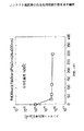
図1は本発明の原理を解説する為のコンタクト抵抗率の合金化時間依存性を表す線図であり、縦軸にはコンタクト抵抗率を、また、横軸には合金化時間をそれぞれ採ってある。
【0012】
このデータを得た試料は、p−GaAsベース層上に厚さが5〔nm〕であるn−GaAsガード・リング層と厚さが25〔nm〕であるn−InGaPエミッタ層の一部を介してPd/Ti/Pt/Auを順に積層成膜し、オーミック・コンタクト電極としたものであって、積層成膜には真空蒸着法を適用した。
【0013】
試料のp−GaAsベース層に於けるキャリヤ濃度は3×10¹⁹〔cm-3〕であり、また、オーミック・コンタクト電極に於ける各金属膜の膜厚は、Pd:30〔nm〕、Ti:40〔nm〕、Pt:40〔nm〕、Au:200〔nm〕である。
【0014】
電極形成時の熱処理温度は400〔℃〕、雰囲気はN2 雰囲気、コンタクト抵抗率の測定はTLM(transmission line mode)法に依った。
【0015】
本発明に於いて、熱処理に依ってコンタクト抵抗率が低下した理由は、半導体層と電極の最下層であるPd層との合金化反応が進行した為である。
【0016】
即ち、Pd層がn−InGaPエミッタ層及びn−GaAsガード・リング層を介してp−GaAsベース層と合金化反応が行なわれた為であり、これについては、Pd層をp−GaAsベース層に直接蒸着した場合にも図1に見られる傾向と同じ傾向を示すことが判っている。
【0018】
前記したところから、本発明に依る三族−五族化合物半導体装置の製造方法に於いては、
(1)
一導電型三族−五族化合物半導体ベース層(例えばp−GaAsベース層5)に積層された反対導電型三族−五族化合物半導体ガード・リング層(例えばn−GaAs第一エミッタ層6)上にPd層及びTi層及びPt層及びAu層の順に積層された積層体からなるべース電極(例えばベース電極11)を形成してから熱処理を行ってPd層と一導電型三族−五族化合物半導体ベース層とを合金化する工程が含まれてなることを特徴とするか、或いは、
【0019】
(2)
反対導電型三族−五族化合物半導体エミッタ層(例えばn−InGaP第二エミッタ層7)をメサ状に加工した際に一部がベース電極形成予定部分を覆う薄膜となって残った前記エミッタ層上にPd層及びTi層及びPt層及びAu層の順に積層された積層体からなるベース電極(例えばベース電極11)を形成してから熱処理を行ってPd層と一導電型三族−五族化合物半導体ベース層(例えばp−GaAsベース層5)とを合金化する工程が含まれてなることを特徴とする。
【0020】
前記手段を採ることに依り、電極と一導電型高濃度不純物含有半導体ベース層とは、良好なオーミック・コンタクトを生成することができ、また、導電型が反対導電型であるガード・リング層上からであっても、熱処理を行なうことで、一導電型高濃度不純物含有半導体ベース層と良好且つ安定にオーミック・コンタクトをとることが可能であって、高速動作する半導体装置に不可欠な低い電極コンタクト抵抗を実現することができる。
【0021】
【発明の実施の形態】
図2は本発明に於ける一実施の形態に依って製造されたHBTを表す要部切断側面図であって、次に、このHBTを製造する方法について説明する。
【0022】
(1)
例えば、MOCVD(metalorganic chemical vapour deposition)法を適用することに依り、基板1上にバッファ層2、サブ・コレクタ層3、コレクタ層4、ベース層5、第一のガード・リングである第一エミッタ層6、第二のガード・リングである第二エミッタ層7、第三エミッタ層8、エミッタ・キャップ層9を成長させる。
【0023】
ここで、各半導体部分に関する主要なデータを例示すると以下の通りである。
(a) 基板1について
材料:半絶縁性GaAs
(b) バッファ層2について
材料:ノンドープGaAs
厚さ:500〔nm〕
(c) サブ・コレクタ層3について
材料:n−GaAs
不純物濃度:5×10¹⁸〔cm-3〕
厚さ:500〔nm〕
(d) コレクタ層4
材料:n−GaAs
不純物濃度:3×10¹⁶〔cm-3〕
厚さ:300〔nm〕
(e) ベース層5について
材料:p−GaAs
不純物濃度:2×10¹⁹〔cm-3〕
厚さ:80〔nm〕
(f) 第一のガード・リングである第一エミッタ層6について
材料:n−InGaP
不純物濃度:3×10¹⁷〔cm-3〕
厚さ:30〔nm〕
(g) 第二のガード・リングである第二エミッタ層7について
材料:n−GaAs
不純物濃度:3×10¹⁷〔cm-3〕
厚さ:10〔nm〕
(h) 第三エミッタ層8について
材料:n−GaAs
不純物濃度:3×10¹⁷〔cm-3〕(下層)→5×10¹⁸〔cm-3〕(上層)のグレーデッド
厚さ:300〔nm〕
(i) エミッタ・キャップ層9について
材料:n−Inx Ga1-x As(x=0〜0.6)
不純物濃度:5×10¹⁸〔cm-3〕〜4×10¹⁹〔cm-3〕
厚さ:100〔nm〕
【0024】
(2)
スパッタリング法を適用することに依り、エミッタ・キャップ層9上に厚さが例えば300〔nm〕であるWSi膜を堆積してから、リソグラフィ技術に於けるレジスト・プロセスを適用することに依って、エミッタ電極パターンのレジスト膜を形成し、その後、ハロゲン系エッチング・ガスを用いるドライ・エッチング法を適用してWSi膜のエッチングを行なってエミッタ電極10を形成する。
【0025】
(3)
エッチャントをリン酸と水の混合液とするウエット・エッチング法を適用することに依り、エミッタ電極10をマスクとしてエミッタ・キャップ層9のエッチングを行ない、ハロゲン系ガスをエッチング・ガスとするドライ・エッチング法を適用することに依り、第三エミッタ層8のエッチングを行ない、第二のガード・リングである第二エミッタ層7が表出された時点でエッチングを停止し、第一段メサ部分形成を終了する。
【0026】
(4)
リソグラフィ技術に於けるレジスト・プロセスを適用することに依り、表出されている第二エミッタ層7に於けるベース電極形成予定部分に開口をもつレジスト膜を形成する。
【0027】
(5)
真空蒸着法及びリフト・オフ法を適用することに依り、厚さが30〔nm〕/40〔nm〕/40〔nm〕/200〔nm〕であるPd/Ti/Pt/Au
からなるベース電極11を形成する。
【0028】
熱処理を実施することで、ベース電極11は、第二エミッタ層7の一部及び第一エミッタ層6を介し、ベース層5と良好にオーミック・コンタクトさせることができる。尚、この熱処理は、他の工程タイミングで実施しても良い。
【0029】
(6)
リソグラフィ技術に於けるレジスト・プロセスを適用することに依り、サブ・コレクタ層3に於けるコレクタ電極形成予定部分を表出させる為の開口をもつレジスト膜を形成する。
【0030】
(7)
エッチャントをリン酸と水の混合液とするウエット・エッチング法を適用することに依り、前記工程(6)で形成したレジスト膜をマスクとして第二のガード・リングである第二エミッタ層7のエッチングを行ない、更に、エッチャントを塩酸と水の混合液とするウエット・エッチング法を適用することに依り、第一のガード・リングである第一エミッタ層6のエッチングを行ない、その後、ハロゲン系ガスをエッチング・ガスとするドライ・エッチング法を適用することに依って、ベース層5、コレクタ層4のエッチングを行ない、サブ・コレクタ層3が表出されたところでエッチングを停止し、第二段メサ部分形成を終了する。
【0031】
(8)
リソグラフィ技術に於けるレジスト・プロセス、真空蒸着法、リフト・オフ法を適用することに依り、厚さが20〔nm〕/100〔nm〕であるAuGe/Auからなるコレクタ電極12を形成する。
【0032】
以上のようにして製造したHBTでは、ベース電極11の最下層のPd層が高濃度p型ベース層5と良好にオーミック・コンタクトする。
【0033】
本発明に於いては、前記実施の形態に限られることなく、他に多くの改変を実現でき、例えば、前記実施の形態では、GaAs/InGaP系HBTについて説明したが、InP/InGaAs系HBTに適用しても有効である。
【0034】
また、前記実施の形態では、p−GaAsベース層5上に第一のガード・リングであるn−InGaP第一エミッタ層6並びに第二のガード・リングであるn−GaAs第二エミッタ層7を形成し、また、第一段メサ部分を形成したことに依って表出される第二段メサ部分の頂面には、n−GaAs第二エミッタ層7を薄く残して覆うように構成してあるが、必要に応じ、第二のガード・リングであるn−GaAs第二エミッタ層7を残さない構成にしたり、或いは、第二のガード・リングであるn−GaAs第二エミッタ層7及び第一のガード・リングであるn−InGaP第一エミッタ層6を省略することもできる。
【0035】
【発明の効果】
本発明に依る三族−五族化合物半導体装置の製造方法に於いては、一導電型三族−五族化合物半導体ベース層上にPd層及びTi層及びPt層及びAu層の順に積層された積層体からなるベース電極を形成してから熱処理を行なってPd層と一導電型三族−五族化合物半導体ベース層とを合金化している。
【0036】
前記構成を採ることに依り、ベース電極と一導電型高濃度不純物含有半導体ベース層とは、良好なオーミック・コンタクトを生成することができ、また、導電型が反対導電型であるガード・リング層上からであっても、熱処理を行なうことで、一導電型高濃度不純物含有半導体ベース層と良好且つ安定にオーミック・コンタクトをとることが可能であって、高速動作する半導体装置に不可欠な低い電極コンタクト抵抗を実現することができる。
【図面の簡単な説明】
【図1】本発明の原理を解説する為のコンタクト抵抗率の合金化時間依存性を表す線図である。
【図2】本発明に於ける一実施の形態であるHBTを表す要部切断側面図である。
【符号の説明】
1 基板
2 バッファ層
3 サブ・コレクタ層
4 コレクタ層
5 ベース層
6 第一エミッタ層(第一のガード・リング)
7 第二エミッタ層(第二のガード・リング)
8 第三エミッタ層
9 エミッタ・キャップ層
10 エミッタ電極
11 ベース電極
12 コレクタ電極[0001]
BACKGROUND OF THE INVENTION
The present invention relates to a method for manufacturing a Group 3-5 group semiconductor device having an electrode with low contact resistance.
[0002]
Currently, in order to promote high speed and large amount of information in optical communication systems and high performance of high speed computers, it is required to improve the performance of compound semiconductor devices. As part of this, reduction of electrode contact resistance has become a problem. Therefore, the present invention discloses a means for solving the problem.
[0003]
[Prior art]
In a conventional compound semiconductor device, particularly a heterojunction bipolar transistor (HBT), p-type impurities such as AuZn, AuMn, and AuBe are used as constituent elements as alloy-type ohmic contact electrodes for p-type compound semiconductor layers. A good ohmic contact is obtained by depositing an alloy film and a multilayer film containing a p-type impurity element on the surface of the semiconductor layer by vacuum deposition and alloying the electrode and the semiconductor interface by a subsequent heat treatment. An electrode is formed. Examples of the multilayer film containing the p-type impurity element include Pd / Zn / Pt / Au and Pd / Zn / Pd / Au. In this case, the p-type impurity element is Zn.
[0004]
However, when the electrode is applied to a p-type thin layer structure like the base electrode in HBT, Au diffuses into each crystal layer from the base layer to the collector layer, resulting in lower contact resistance and lower device reliability. May be invited.
[0005]
Recently, as an electrode that can obtain a low contact resistance and a long life, a technique of applying a laminated structure made of Pt / Ti / Pt / Au to the p-type base layer of HBT has been disclosed (if necessary, “ Japanase Journal of Appl. Phys. L558-560 (1991) Okada et al.
[0006]
In the electrode having a laminated structure made of Pt / Ti / Pt / Au, when the first reaction layer with the semiconductor layer is a Pt layer and a natural oxide film exists between the semiconductor layer and the Pt layer, The alloying of the layer and the Pt layer is not sufficiently performed, and it is difficult to realize low contact resistance with good reproducibility.
[0007]
Furthermore, a laminate structure made of Pd / Zn / Pt / Au is used for the base electrode of HBT (if necessary, “JP-A-5-259435”, “JP-A-6-310706”, etc.) See).
[0008]
In an electrode having a laminated structure of Pd / Zn / Pt / Au, Zn diffuses into the semiconductor layer side and the surface side while Pt penetrates into the Pd layer in the heat treatment step of alloying the semiconductor layer and the electrode. , Au diffuses through the Pt layer, which is a barrier layer, and it is difficult to ensure the reliability of the electrode.
[0009]
[Problems to be solved by the invention]
In the present invention, only a simple modification is made to the stacking order of known electrode materials, without being affected by a semiconductor layer which is a natural oxide film on the surface of the semiconductor layer or a guard ring on the base layer. A low contact resistance is realized with good reproducibility, and the effect of the barrier layer formed between the metal layers can be sufficiently exhibited.
[0010]
[Means for Solving the Problems]
In the present invention, Pd, Ti, Pt, and Au, which are known as electrode materials for semiconductor devices using a Group 3-5 group compound semiconductor, are used, and Pd is laminated in the order described above with the semiconductor layer side. By using Pd as a metal that reacts with the semiconductor layer, that is, alloying alloy, a low contact resistance is maintained, and a Ti layer serving as an effective barrier layer against Pt is interposed between the Pd layer and the Pt layer. Basically, Pt is prevented from excessively penetrating the Pd layer by heat treatment during electrode formation.
[0011]
FIG. 1 is a diagram showing the dependence of contact resistivity on alloying time for explaining the principle of the present invention. The vertical axis represents contact resistivity and the horizontal axis represents alloying time. is there.
[0012]
The sample from which this data was obtained consists of an n-GaAs guard ring layer having a thickness of 5 nm and a part of an n-InGaP emitter layer having a thickness of 25 nm on the p-GaAs base layer. Then, Pd / Ti / Pt / Au were sequentially laminated to form ohmic contact electrodes, and vacuum deposition was applied to the laminated film.
[0013]
The carrier concentration in the p-GaAs base layer of the sample is 3 × 10 19 [cm −3 ], and the film thickness of each metal film in the ohmic contact electrode is Pd: 30 [nm], Ti : 40 [nm], Pt: 40 [nm], Au: 200 [nm].
[0014]
The heat treatment temperature at the time of electrode formation was 400 [° C.], the atmosphere was an N 2 atmosphere, and the contact resistivity was measured by the TLM (transmission line mode) method.
[0015]
In the present invention, the reason why the contact resistivity is lowered by the heat treatment is that the alloying reaction between the semiconductor layer and the Pd layer, which is the lowermost layer of the electrode, proceeds.
[0016]
That is, the Pd layer was alloyed with the p-GaAs base layer via the n-InGaP emitter layer and the n-GaAs guard ring layer. It is known that the same tendency as that shown in FIG.
[0018]
From the foregoing, in the method for manufacturing a Group III-V Group compound semiconductor device according to the present invention,
(1)
Opposite conductivity type III-V compound semiconductor guard ring layer (for example, n-GaAs first emitter layer 6) stacked on one conductivity type III-V compound semiconductor base layer (for example, p-GaAs base layer 5) A base electrode (for example, the base electrode 11) made of a laminate in which a Pd layer, a Ti layer, a Pt layer, and an Au layer are laminated in this order is formed, and then heat treatment is performed, so that the Pd layer and one conductivity type group III- Or a step of alloying the
[0019]
(2)
The emitter layer which remains as a thin film partially covering a base electrode formation scheduled portion when an opposite conductivity type group 3-5 group compound semiconductor emitter layer (for example, n-InGaP second emitter layer 7) is processed into a mesa shape A base electrode (for example, base electrode 11) made of a laminate in which a Pd layer, a Ti layer, a Pt layer, and an Au layer are laminated in this order is formed, and then heat treatment is performed, and then the Pd layer and one conductivity type Group 3-5 group are formed. A step of alloying a compound semiconductor base layer (for example, p-GaAs base layer 5) is included.
[0020]
By adopting the above means, the electrode and the one-conductivity-type high-concentration-contained semiconductor base layer can form a good ohmic contact, and on the guard ring layer whose conductivity type is the opposite conductivity type. Even if the heat treatment is performed, it is possible to make a good and stable ohmic contact with the semiconductor base layer containing one conductivity type high-concentration impurity, and the low electrode contact essential for a semiconductor device operating at high speed. Resistance can be realized.
[0021]
DETAILED DESCRIPTION OF THE INVENTION
FIG. 2 is a cut-away side view showing the main part of the HBT manufactured according to the embodiment of the present invention. Next, a method for manufacturing the HBT will be described.
[0022]
(1)
For example, a
[0023]
Here, main data regarding each semiconductor portion is exemplified as follows.
(A) Substrate 1 Material: Semi-insulating GaAs
(B)
Thickness: 500 [nm]
(C)
Impurity concentration: 5 × 10 18 [cm −3 ]
Thickness: 500 [nm]
(D) Collector layer 4
Material: n-GaAs
Impurity concentration: 3 × 10 16 [cm −3 ]
Thickness: 300 [nm]
(E) About
Impurity concentration: 2 × 10 19 [cm −3 ]
Thickness: 80 [nm]
(F) About the first emitter layer 6 which is the first guard ring Material: n-InGaP
Impurity concentration: 3 × 10 17 [cm −3 ]
Thickness: 30 [nm]
(G) Material for the second emitter layer 7 which is the second guard ring: n-GaAs
Impurity concentration: 3 × 10 17 [cm −3 ]
Thickness: 10 [nm]
(H) Material for the third emitter layer 8: n-GaAs
Impurity concentration: 3 × 10 17 [cm −3 ] (lower layer) → graded thickness of 5 × 10 18 [cm −3 ] (upper layer): 300 [nm]
(I) About the
Impurity concentration: 5 × 10 18 [cm −3 ] to 4 × 10 19 [cm −3 ]
Thickness: 100 [nm]
[0024]
(2)
By depositing a WSi film having a thickness of, for example, 300 nm on the
[0025]
(3)
By applying a wet etching method using an etchant mixture of phosphoric acid and water, the
[0026]
(4)
By applying a resist process in the lithography technique, a resist film having an opening at a portion where the base electrode is to be formed in the exposed second emitter layer 7 is formed.
[0027]
(5)
Pd / Ti / Pt / Au having a thickness of 30 [nm] / 40 [nm] / 40 [nm] / 200 [nm] by applying a vacuum deposition method and a lift-off method
A
[0028]
By performing the heat treatment, the
[0029]
(6)
By applying a resist process in the lithography technique, a resist film having an opening for exposing a collector electrode formation scheduled portion in the
[0030]
(7)
Etching of the second emitter layer 7 as the second guard ring by applying the wet etching method using the etchant as a mixture of phosphoric acid and water, using the resist film formed in the step (6) as a mask. In addition, by applying a wet etching method in which an etchant is a mixture of hydrochloric acid and water, the first emitter layer 6 which is the first guard ring is etched, and then a halogen-based gas is added. By applying a dry etching method using an etching gas, the
[0031]
(8)
The
[0032]
In the HBT manufactured as described above, the lowermost Pd layer of the
[0033]
The present invention is not limited to the above embodiment, and many other modifications can be realized. For example, in the above embodiment, the GaAs / InGaP HBT has been described, but the InP / InGaAs HBT has been described. It is effective even when applied.
[0034]
In the embodiment, the n-InGaP first emitter layer 6 as the first guard ring and the n-GaAs second emitter layer 7 as the second guard ring are formed on the p-
[0035]
【The invention's effect】
In the method for manufacturing a Group 3-5 group semiconductor device according to the present invention, a Pd layer, a Ti layer, a Pt layer, and an Au layer are stacked in this order on the one conductivity type Group 3-5 group semiconductor base layer. After the base electrode made of the laminate is formed, heat treatment is performed to alloy the Pd layer and the one-conductivity type Group 3-5 group semiconductor base layer.
[0036]
By adopting the above configuration, the base electrode and the one-conductivity type high-concentration impurity-containing semiconductor base layer can form a good ohmic contact, and the guard ring layer whose conductivity type is the opposite conductivity type Even from the top, by performing heat treatment, it is possible to make a good and stable ohmic contact with the semiconductor base layer containing one conductivity type high concentration impurity, and a low electrode that is indispensable for a semiconductor device operating at high speed Contact resistance can be realized.
[Brief description of the drawings]
FIG. 1 is a diagram showing the alloying time dependence of contact resistivity for explaining the principle of the present invention.
FIG. 2 is a cut-away side view of an essential part showing an HBT according to one embodiment of the present invention.
[Explanation of symbols]
1
7 Second emitter layer (second guard ring)
8
Claims (2)
が含まれてなることを特徴とする三族−五族化合物半導体装置の製造方法。A laminate in which a Pd layer, a Ti layer, a Pt layer, and an Au layer are laminated in this order on the opposite conductivity type Group 3-5 group compound semiconductor guard ring layer laminated on the one conductivity type Group 3-5 group semiconductor base layer Forming a base electrode made of the alloy, and then performing a heat treatment to alloy the Pd layer with the one-conductivity type Group-3 Group-5 semiconductor base layer. A method for manufacturing a group compound semiconductor device.
が含まれてなることを特徴とする三族−五族化合物半導体装置の製造方法。A Pd layer, a Ti layer, a Pt layer, and a Pd layer are formed on the emitter layer that remains as a thin film that covers a portion where the base electrode is to be formed when the opposite conductivity type Group-3-5 compound semiconductor emitter layer is processed into a mesa shape. Forming a base electrode composed of a laminated body in the order of the Au layer and then performing a heat treatment to alloy the Pd layer and the one-conductivity-type group-3 / group-5 compound semiconductor base layer. A method for producing a group III-V group compound semiconductor device.
Priority Applications (1)
| Application Number | Priority Date | Filing Date | Title |
|---|---|---|---|
| JP02803798A JP3876397B2 (en) | 1998-02-10 | 1998-02-10 | Method for manufacturing a Group III-V Group compound semiconductor device |
Applications Claiming Priority (1)
| Application Number | Priority Date | Filing Date | Title |
|---|---|---|---|
| JP02803798A JP3876397B2 (en) | 1998-02-10 | 1998-02-10 | Method for manufacturing a Group III-V Group compound semiconductor device |
Publications (2)
| Publication Number | Publication Date |
|---|---|
| JPH11233452A JPH11233452A (en) | 1999-08-27 |
| JP3876397B2 true JP3876397B2 (en) | 2007-01-31 |
Family
ID=12237549
Family Applications (1)
| Application Number | Title | Priority Date | Filing Date |
|---|---|---|---|
| JP02803798A Expired - Fee Related JP3876397B2 (en) | 1998-02-10 | 1998-02-10 | Method for manufacturing a Group III-V Group compound semiconductor device |
Country Status (1)
| Country | Link |
|---|---|
| JP (1) | JP3876397B2 (en) |
Families Citing this family (1)
| Publication number | Priority date | Publication date | Assignee | Title |
|---|---|---|---|---|
| WO2020010592A1 (en) * | 2018-07-12 | 2020-01-16 | Shenzhen Xpectvision Technology Co., Ltd. | A radiation detector |
-
1998
- 1998-02-10 JP JP02803798A patent/JP3876397B2/en not_active Expired - Fee Related
Also Published As
| Publication number | Publication date |
|---|---|
| JPH11233452A (en) | 1999-08-27 |
Similar Documents
| Publication | Publication Date | Title |
|---|---|---|
| US20020027232A1 (en) | Hbt having a carbon-doped gaasbsb base contact layer | |
| US6462362B1 (en) | Heterojunction bipolar transistor having prevention layer between base and emitter | |
| JP3294461B2 (en) | Heterojunction bipolar transistor and manufacturing method thereof | |
| JP3087671B2 (en) | Bipolar transistor and method of manufacturing the same | |
| JP3876397B2 (en) | Method for manufacturing a Group III-V Group compound semiconductor device | |
| JP2002299603A (en) | Semiconductor device | |
| JPH0945890A (en) | Ohmic electrode structure, semiconductor device and manufacturing method thereof | |
| JP3349267B2 (en) | Hetero bipolar semiconductor device and method of manufacturing the same | |
| JP3057679B2 (en) | Heterojunction bipolar transistor and manufacturing method thereof | |
| JP3358901B2 (en) | Method for manufacturing compound semiconductor device | |
| JP2890729B2 (en) | Bipolar transistor and method of manufacturing the same | |
| JP2001217255A (en) | Heterojunction bipolar transistor, method of manufacturing the same, and communication device | |
| JP3863270B2 (en) | Semiconductor device and manufacturing method thereof | |
| JPH0422344B2 (en) | ||
| JP4092597B2 (en) | Semiconductor device and manufacturing method thereof | |
| JPH098055A (en) | Hetero-bipolar semiconductor device and manufacturing method thereof | |
| JPH10303214A (en) | Hetero bipolar semiconductor device and method of manufacturing the same | |
| JP3624357B2 (en) | Method for manufacturing heterojunction bipolar transistor | |
| JP2001085741A (en) | Semiconductor device and light emitting semiconductor device | |
| JP2830409B2 (en) | Bipolar transistor and method of manufacturing the same | |
| JP2592277B2 (en) | Manufacturing method of bipolar semiconductor device | |
| JP2611474B2 (en) | Method for manufacturing compound semiconductor device | |
| JP3349644B2 (en) | Compound semiconductor device and method of manufacturing the same | |
| JP3201024B2 (en) | Method for manufacturing semiconductor device | |
| JPH11121463A (en) | Semiconductor device |
Legal Events
| Date | Code | Title | Description |
|---|---|---|---|
| A621 | Written request for application examination |
Free format text: JAPANESE INTERMEDIATE CODE: A621 Effective date: 20050209 |
|
| A977 | Report on retrieval |
Free format text: JAPANESE INTERMEDIATE CODE: A971007 Effective date: 20060628 |
|
| A131 | Notification of reasons for refusal |
Free format text: JAPANESE INTERMEDIATE CODE: A131 Effective date: 20060704 |
|
| A521 | Request for written amendment filed |
Free format text: JAPANESE INTERMEDIATE CODE: A523 Effective date: 20060901 |
|
| TRDD | Decision of grant or rejection written | ||
| A01 | Written decision to grant a patent or to grant a registration (utility model) |
Free format text: JAPANESE INTERMEDIATE CODE: A01 Effective date: 20061003 |
|
| A61 | First payment of annual fees (during grant procedure) |
Free format text: JAPANESE INTERMEDIATE CODE: A61 Effective date: 20061019 |
|
| R150 | Certificate of patent or registration of utility model |
Free format text: JAPANESE INTERMEDIATE CODE: R150 |
|
| FPAY | Renewal fee payment (event date is renewal date of database) |
Free format text: PAYMENT UNTIL: 20101110 Year of fee payment: 4 |
|
| FPAY | Renewal fee payment (event date is renewal date of database) |
Free format text: PAYMENT UNTIL: 20101110 Year of fee payment: 4 |
|
| FPAY | Renewal fee payment (event date is renewal date of database) |
Free format text: PAYMENT UNTIL: 20111110 Year of fee payment: 5 |
|
| FPAY | Renewal fee payment (event date is renewal date of database) |
Free format text: PAYMENT UNTIL: 20111110 Year of fee payment: 5 |
|
| FPAY | Renewal fee payment (event date is renewal date of database) |
Free format text: PAYMENT UNTIL: 20121110 Year of fee payment: 6 |
|
| FPAY | Renewal fee payment (event date is renewal date of database) |
Free format text: PAYMENT UNTIL: 20121110 Year of fee payment: 6 |
|
| FPAY | Renewal fee payment (event date is renewal date of database) |
Free format text: PAYMENT UNTIL: 20131110 Year of fee payment: 7 |
|
| LAPS | Cancellation because of no payment of annual fees |