JP3888112B2 - Ultrasonic beauty device - Google Patents
Ultrasonic beauty device Download PDFInfo
- Publication number
- JP3888112B2 JP3888112B2 JP2001288950A JP2001288950A JP3888112B2 JP 3888112 B2 JP3888112 B2 JP 3888112B2 JP 2001288950 A JP2001288950 A JP 2001288950A JP 2001288950 A JP2001288950 A JP 2001288950A JP 3888112 B2 JP3888112 B2 JP 3888112B2
- Authority
- JP
- Japan
- Prior art keywords
- circuit
- ultrasonic
- ultrasonic transducer
- supplied
- voltage
- Prior art date
- Legal status (The legal status is an assumption and is not a legal conclusion. Google has not performed a legal analysis and makes no representation as to the accuracy of the status listed.)
- Expired - Fee Related
Links
- 230000003796 beauty Effects 0.000 title 1
- 238000001514 detection method Methods 0.000 claims description 90
- 239000002537 cosmetic Substances 0.000 claims description 44
- 230000005855 radiation Effects 0.000 claims description 9
- 239000000523 sample Substances 0.000 claims description 9
- 230000000638 stimulation Effects 0.000 claims description 7
- 230000005284 excitation Effects 0.000 claims description 4
- 238000010586 diagram Methods 0.000 description 26
- 230000010355 oscillation Effects 0.000 description 23
- 230000003321 amplification Effects 0.000 description 15
- 238000003199 nucleic acid amplification method Methods 0.000 description 15
- 230000007423 decrease Effects 0.000 description 3
- 230000006870 function Effects 0.000 description 3
- 239000003990 capacitor Substances 0.000 description 2
- WABPQHHGFIMREM-UHFFFAOYSA-N lead(0) Chemical compound [Pb] WABPQHHGFIMREM-UHFFFAOYSA-N 0.000 description 2
- 238000000034 method Methods 0.000 description 2
- 230000005856 abnormality Effects 0.000 description 1
- 230000004397 blinking Effects 0.000 description 1
- 238000006243 chemical reaction Methods 0.000 description 1
- 238000009499 grossing Methods 0.000 description 1
- 239000004973 liquid crystal related substance Substances 0.000 description 1
- 238000012986 modification Methods 0.000 description 1
- 230000004048 modification Effects 0.000 description 1
- 230000008447 perception Effects 0.000 description 1
Images





Landscapes
- Percussion Or Vibration Massage (AREA)
Description
【0001】
【発明の属する技術分野】
本発明は、超音波振動子が取り付けられてなる振動部を顔等の肌に接触させることにより肌に超音波刺激を付与するようにした超音波美容器に関する。
【0002】
【従来の技術】
近年、プローブの先端部に配設されたホーンに超音波振動子が接合されてなる振動部を、顔等の肌に接触させることにより肌に超音波振動(超音波刺激)を付与するようにした超音波美容器が知られている。図12は、従来の超音波美容器の構成図である。(a)は、全体構成図であり、(b)は、後述する振動部の拡大構成図である。超音波美容器は、超音波を発生させる超音波振動子1と、放射面22を肌に接触させると共に接合面21で超音波振動子1に接合されたホーン2とからなる振動部10と振動部10を固定すると共に利用者によって把持されるハウジング31とを備えたプローブ3と、超音波振動子1にプローブコード32及びリード線11を介して電力を供給することによって駆動する駆動部4とを備えている。
【0003】
【発明が解決しようとする課題】
上述のような超音波美容器を用いる際に、プローブ3と駆動部4との間に無理な張力を加えた場合には、プローブコード32が断線することがある。また、プローブ3を床面上等に落下させた場合には、衝撃によってリード線11と超音波振動子1の電極との接合が外れたり、超音波振動子1が破損することがある。このような場合には、駆動部4から超音波振動子1に所期の電力が供給されないため、ホーン2から肌に本来のあるいは全く超音波振動(超音波刺激)を付与することはできない。
【0004】
しかしながら、超音波美容器の利用者は、超音波振動の特性から、ホーン2から肌に対して超音波振動(超音波刺激)が付与されているか否かを触覚(振動の知覚)・聴覚(振動音の知覚)等によって判断することが困難であるため、駆動部4から超音波振動子1に電力が供給されていない状態であるにも拘らず、超音波美容器を継続して使用することがあった。
【0005】
本発明は、上記の課題に鑑みてなされたもので、超音波振動子に電力が供給されているか否かを容易に確認することが可能な超音波美容器を提供することを目的とする。
【0006】
【課題を解決するための手段】
本発明による超音波美容器は、肌に超音波刺激を付与する超音波美容器であって、超音波を発生させる超音波振動子と、接合面で前記超音波振動子に接合され、放射面から超音波を肌に付与するホーンとからなる振動部を備えたプローブと、前記超音波振動子に励振用の電力を供給する駆動手段と、前記駆動手段から前記超音波振動子へ電力が供給されているか否かを検出する検出手段と、前記検出手段による検出結果を報知する報知手段とを備え、前記駆動手段は、前記超音波振動子を駆動する周波数である駆動周波数を変更する周波数変更手段を備え、前記検出手段は、前記駆動手段から前記超音波振動子へ供給される駆動電流を検出することによって前記超音波振動子へ電力が供給されているか否かを検出するものであり、前記周波数変更手段による駆動周波数の変更に伴う前記駆動電流の変化を検出することによって前記超音波振動子へ電力が供給されているか否かを検出することを特徴としている。
【0007】
上記の構成によれば、駆動手段によって、超音波振動子に励振用の電力が供給され、超音波振動子によって、超音波が発生され、ホーンによって、放射面から超音波が肌に付与される。検出手段によって、駆動手段から超音波振動子へ電力が供給されているか否かが検出され、報知手段によって、検出手段による検出結果が報知されるため、超音波振動子に電力が供給されているか否かを容易に確認することが可能となる。
【0009】
また、上記の構成によれば、検出手段によって、駆動手段から超音波振動子へ供給される駆動電流を検出することによって超音波振動子へ電力が供給されているか否かが検出されるため、超音波振動子に電力が供給されているか否かを簡単な回路構成で検出することが可能となる。
【0010】
また、上記の構成によれば、周波数変更手段によって、超音波振動子を駆動する周波数である駆動周波数が変更され、検出手段によって、周波数変更手段による駆動周波数の変更に伴う駆動電流の変化を検出することにより超音波振動子へ電力が供給されているか否かが検出されるため、駆動手段がノイズ対策のためのLC回路等からなるフィルタ回路を備える場合にも超音波振動子へ電力が供給されているか否かを検出することができる。
【0011】
【発明の実施の形態】
(第1実施形態:請求項1に記載の超音波美容器の実施形態の一例)
図1は、本発明の第1実施形態に係る超音波美容器の構成図である。超音波美容器は、超音波を発生させる超音波振動子1と、放射面を肌に接触させると共に接合面で超音波振動子1に接合されたホーン2とからなる振動部10と、超音波振動子1に電力を供給することによって駆動する駆動部4(駆動手段に相当する)と、駆動部4から超音波振動子1へ電力が供給されているか否かを検出する検出部5(検出手段に相当する)と、検出部5による検出結果を表示する表示部6(報知手段に相当する)とを備えている。
【0012】
駆動部4は、高周波信号を発生する発振回路41と、発振回路41にて発生された高周波信号を増幅する増幅回路42とを備えている。検出部5は、駆動部4から超音波振動子1に供給される電流を電圧の形で出力するものである。なお、本実施形態では、電流と電圧との関係を後述するように、反転増幅手段等を介して反転させている。表示部6は、検出部5からの検出信号を所定の基準電圧と比較して基準電圧以上である場合に表示回路62へ表示信号を出力する表示制御回路61と、表示制御回路61からの表示信号を受けて検出部5の検出結果を表示する表示回路62とを備えている。報知手段としての表示回路62としては、例えば、LED点灯回路が採用可能である。
【0013】
図2は、第1実施形態の超音波美容器の動作を説明するための波形図である。(a)は超音波振動子1に付与される電圧の波形であり、(b)は超音波振動子1に流れる電流の波形であり、(c)は検出部5の出力電圧の波形であり、(d)は表示制御回路61の入力電圧の波形であり、(e)は表示回路62の出力の波形である。図の横軸は時間であって、横軸方向の略中央部の時間T1の左側が駆動部4から超音波振動子1へ電力が供給されている状態(駆動状態という)であり、時間T1の右側が、断線等の原因によって駆動部4から超音波振動子1へ電力が供給されていない状態(非駆動状態という)である。
【0014】
駆動状態においては、所定の電流が超音波振動子1に流れ、検出部5の出力電圧及び表示制御回路61の入力電圧は、基準電圧より低い電圧となり、表示制御回路61によって表示信号は出力されず、表示回路62によってLEDは消灯状態となる。非駆動状態においては、電流が超音波振動子1に流れず、検出部5の出力電圧及び表示制御回路61の入力電圧は、基準電圧より高い電圧となり、表示制御回路61によって表示信号が出力され、表示回路62によってLEDが点灯状態となる。
【0015】
検出部5によって、駆動部4から超音波振動子1へ電力が供給されているか否かが検出され、表示部6によって、検出部5による検出結果がLEDに表示されるため、超音波振動子に電力が供給されているか否かを容易に確認することが可能となる。特に、非駆動状態において、LEDを点灯させるため、異常確認が容易となる。
【0016】
(第2実施形態:請求項2に記載の超音波美容器の実施形態の一例)
図3は、本発明の第2実施形態に係る超音波美容器の回路図である。超音波美容器は、超音波を発生させる超音波振動子1と、放射面を肌に接触させると共に接合面で超音波振動子1に接合されたホーン2とからなる振動部10と、超音波振動子1に電力を供給することによって駆動する駆動部4A(駆動手段に相当する)と、駆動部4Aから超音波振動子1へ電力が供給されているか否かを検出する検出部5A(検出手段に相当する)と、検出部5Aによる検出結果を表示する表示部6A(報知手段に相当する)とを備えている。
【0017】
駆動部4Aは、高周波電圧を発生する発振回路41Aと、発振回路41Aにて発生された高周波電圧を増幅する増幅回路42Aとを備えている。増幅回路42Aは、プッシュプル回路と直流定電圧電源とを備えている。検出部5Aは、超音波振動子1に流れる電流を電圧に変換して出力するものであって、超音波振動子1に流れる電流を電圧に変換する電流検出回路51Aと、電流検出回路51Aの出力信号を包絡線検波する(高周波成分除去用の平滑回路等からなる)包絡線検波回路52Aと、包絡線検波回路52Aの出力を反転増幅する信号増幅回路53Aとを備えている。電流検出回路51Aは、カレントトランスと抵抗とを備えている。
【0018】
表示部6Aは、検出部5A(信号増幅回路53A)からの検出信号を所定の基準電圧と比較して基準電圧以上である場合に表示回路62Aへ表示信号を出力するコンパレータを有する表示制御回路61Aと、表示制御回路61Aからの表示信号を受けて検出部5Aの検出結果を表示する表示回路62Aとを備えている。ここでは、表示回路62Aは、LED点灯回路からなるものである。
【0019】
図4は、第2実施形態の超音波美容器の動作を説明するための波形図である。(a)は超音波振動子1に付与される電圧の波形であり、(b)は超音波振動子1に流れる電流の波形であり、(c)は電流検出回路51Aの出力電圧の波形であり、(d)は包絡線検波回路52Aの出力電圧の波形であり、(e)は信号増幅回路53Aの出力の波形であり、(f)は表示制御回路61Aの入力電圧であり、(g)は表示制御回路61Aの出力電圧であり、(h)は表示回路62Aの出力である。図の横軸は時間であって、横軸方向の略中央部の時間TAの左側が駆動部4から超音波振動子1へ電力が供給されている状態(駆動状態という)であり、時間TAの右側が、断線等の原因によって駆動部4から超音波振動子1へ電力が供給されていない状態(非駆動状態という)である。
【0020】
駆動状態においては、所定の電流が超音波振動子1に流れ、電流検出回路51Aの出力電圧が0でない所定の値となり、包絡線検波回路52Aの出力電圧が0ではない所定の値となり、信号増幅回路53Aの出力電圧及び表示制御回路61Aの入力電圧が基準電圧より低い電圧となるため、表示制御回路61Aによって表示信号は出力されず(出力が5Vとなり)、表示回路62Aのスイッチ用トランジスタがオフしたままとなるのでLEDには電源からの電流が流れず、LEDは消灯状態となる。
【0021】
非駆動状態においては、電流が超音波振動子1に流れず、電流検出回路51Aの出力電圧及び包絡線検波回路52Aの出力電圧が0となり、信号増幅回路53Aの出力電圧及び表示制御回路61Aの入力電圧が基準電圧より高い電圧となるため、表示制御回路61Aによって表示信号が出力され(出力が0Vとなり)、表示回路62Aのスイッチ用トランジスタがオンして電源からLEDに電流が流れるので、LEDが点灯状態となる。
【0022】
検出部5A(電流検出回路51A)によって、超音波振動子1を流れる電流を検出することによって超音波振動子1へ電力が供給されているか否かが検出されるため、超音波振動子1に電力が供給されているか否かを精度良く検出することが可能となる。
【0023】
(第3実施形態:請求項3に記載の超音波美容器の実施形態の一例)
図5は、本発明の第3実施形態に係る超音波美容器の回路図である。超音波美容器は、超音波を発生させる超音波振動子1と、放射面を肌に接触させると共に接合面で超音波振動子1に接合されたホーン2とからなる振動部10と、超音波振動子1に電力を供給することによって駆動する駆動部4B(駆動手段に相当する)と、駆動部4Bから超音波振動子1へ電力が供給されているか否かを検出する検出部5B(検出手段に相当する)と、検出部5Bによる検出結果を表示する表示部6B(報知手段に相当する)とを備えている。
【0024】
駆動部4Bは、高周波電圧を発生する発振回路41Bと、発振回路41Bにて発生された高周波電圧を増幅する増幅回路42Bとを備えている。増幅回路42Bは、プッシュプル回路と直流定電圧電源とを備えている。検出部5Bは、増幅回路42Bの直流定電圧電源の出力電流を検出して、電圧に変換して出力するものであって、増幅回路42Bの直流定電圧電源の出力電流を検出する抵抗からなる電流検出回路54Bと、電流検出回路54Bによって検出された電圧を反転増幅する信号増幅回路55Bとを備えている。増幅回路42Bの直流定電圧電源の出力電流は、直流定電圧電源の出力側の電解コンデンサによって平滑化されるため、直流電流となり、電流検出回路54Bの出力電圧(抵抗の両端の電圧)は直流電圧となる。電流検出回路54Bは、増幅回路42Bの直流定電圧電源とプッシュプル回路との間に介在され、プッシュプル回路に流入する電流を両端の電圧として検出する抵抗からなるものである。
【0025】
表示部6Aは、検出部5B(信号増幅回路55B)からの検出信号を所定の基準電圧と比較して基準電圧以上である場合に表示回路62Bへ表示信号を出力するコンパレータからなる表示制御回路61Bと、表示制御回路61Bからの表示信号を受けて検出部5Bの検出結果を表示する表示回路62Bとを備えている。ここでは、表示回路62Bは、LED点灯回路からなるものである。
【0026】
図6は、第3実施形態の超音波美容器の動作を説明するための波形図である。(a)は超音波振動子1に付与される電圧の波形であり、(b)は超音波振動子1に流れる電流の波形であり、(c)は増幅回路42Bの直流定電圧電源の出力電流の波形であり、(d)は電流検出回路54Bの出力電圧の波形であり、(e)は信号増幅回路55Bの出力電圧の波形であり、(f)は表示制御回路61Bの入力電圧であり、(g)は表示制御回路61Bの出力電圧であり、(h)は表示回路62Bの出力である。図の横軸は時間であって、横軸方向の略中央部の時間TBの左側が駆動部4Bから超音波振動子1へ電力が供給されている状態(駆動状態という)であり、時間TBの右側が、断線等の原因によって駆動部4から超音波振動子1へ電力が供給されていない状態(非駆動状態という)である。
【0027】
駆動状態においては、所定の電流が超音波振動子1に流れ、増幅回路42Bの直流定電圧電源の出力電流及び電流検出回路54Bの出力電圧が0でない所定の値となり、信号増幅回路53Aの出力電圧及び表示制御回路61Bの入力電圧が、基準電圧より低い電圧となるため、表示制御回路61Bによって表示信号は出力されず(出力が5Vとなり)、表示回路62Bのスイッチ用トランジスタがオフしたままとなるのでLEDには電源からの電流が流れず、LEDは消灯状態となる。
【0028】
非駆動状態においては、電流が超音波振動子1に流れず、増幅回路42Bの直流定電圧電源の出力電流及び電流検出回路54Bの出力電圧が0となり、信号増幅回路53Bの出力電圧及び表示制御回路61Bの入力電圧が、基準電圧より高い電圧となるため、表示制御回路61Bによって表示信号が出力され(出力が0Vとなり)、表示回路62Bのスイッチ用トランジスタがオンして電源からLEDに電流が流れるので、LEDが点灯状態となる。
【0029】
検出部5B(電流検出回路54B)によって、駆動部4Bから超音波振動子1へ供給する電流である駆動電流を検出することによって超音波振動子1へ電力が供給されているか否かが検出されるため、第3実施形態のように高周波電流を増幅する必要がなく、簡単な回路構成で超音波振動子1に電力が供給されているか否かを検出することが可能となる。
【0030】
(第4実施形態:請求項4に記載の超音波美容器の実施形態の一例)
図7は、本発明の第4実施形態に係る超音波美容器の回路図である。超音波美容器は、超音波を発生させる超音波振動子1と、放射面を肌に接触させると共に接合面で超音波振動子1に接合されたホーン2とからなる振動部10と、超音波振動子1に電力を供給することによって駆動する駆動部4C(駆動手段に相当する)と、駆動部4Cから超音波振動子1へ電力が供給されているか否かを検出する検出部5C(検出手段に相当する)と、検出部5Cによる検出結果を表示する表示部6C(報知手段に相当する)とを備えている。
【0031】
駆動部4Cは、高周波電圧を発生するPLL回路からなる発振回路41Cと、発振回路41Cにて発生された高周波電圧を増幅する増幅回路42Cとを備えている。増幅回路42Cは、プッシュプル回路と直流定電圧電源とノイズを除去するフィルタ回路421Cとを備えている。検出部5Cは、増幅回路42Cの直流定電圧電源の出力電流を検出して、電圧に変換して出力するものであって、増幅回路42Cの直流定電圧電源の出力電流を検出する抵抗からなる電流検出回路54Cと、電流検出回路54Cによって検出された電流を電圧に変換して反転増幅する信号増幅回路55Cとを備えている。増幅回路42Cの直流定電圧電源の出力電流は、直流定電圧電源の出力側の電解コンデンサによって平滑化されるため、直流電流となり、電流検出回路54Cの出力電圧(抵抗の両端の電圧)は直流電圧となる。
【0032】
表示部6Cは、後述する発振回路41Cの発振周波数を変更する前後の表示制御回路61Cの入力電圧の変化量ΔVを算出し、この変化量ΔVが所定の基準値ΔV0未満の場合に表示回路62Cへ表示信号を出力すると共にA/D変換機能を有するマイクロコンピュータMCを備えた表示制御回路61Cと、表示制御回路61Cからの表示信号を受けて検出部5Cの検出結果を表示する表示回路62Cとを備えている。ここでは、表示回路62Cは、LED点灯回路からなるものである。なお、表示制御回路61CのマイクロコンピュータMCは、発振回路41Cの発振周波数を設定及び後述する手順に従って変更する機能を有する。すなわち、表示制御回路61CのマイクロコンピュータMCが周波数変更手段に相当する。
【0033】
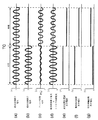
図8は、第4実施形態の超音波美容器の動作を説明するための波形図である。(a)は超音波振動子1に付与される電圧の波形であり、(b)は超音波振動子1に流れる電流の波形であり、(c)はフィルタ回路421Cから接地側に流れる電流の波形であり、(d)は超音波振動子1に流れる電流とフィルタ回路421Cから接地側に流れる電流との和(すなわち、フィルタ回路421Cに流れる電流)の波形であり、(e)は増幅回路42Cの直流定電圧電源の出力電流の波形であり、(f)は電流検出回路54Cの出力電圧の波形であり、(g)は信号増幅回路55Cの出力電圧の波形である。図の横軸は時間であって、横軸方向の略中央部の時間TCの左側が駆動部4Cから超音波振動子1へ電力が供給されている状態(駆動状態という)であり、時間TCの右側が、断線等の原因によって駆動部4から超音波振動子1へ電力が供給されていない状態(非駆動状態という)である。
【0034】
駆動状態においては、所定の電流がフィルタ回路421C及び超音波振動子1に流れ、増幅回路42Cの直流定電圧電源の出力電流が0でない所定の値となり、電流検出回路54Cの出力電圧及び信号増幅回路55Cの出力電圧が所定の値となる。一方、非駆動状態においては、超音波振動子1には電流が流れないが、フィルタ回路421Cから接地側には電流が流れるため、増幅回路42Cの直流定電圧電源の出力電流が及び電流検出回路54Cの出力電圧が0でない所定の値となる。なお、フィルタ回路421Cに流れる電流の値は、発振回路41C側からフィルタ回路421C側を見たインピーダンスによって決定するため、図のように非駆動状態の場合のほうが駆動状態よりも電流値が増大する場合がある。このように、非駆動状態においても、フィルタ回路421Cに電流が流れるため、増幅回路42Cの直流定電圧電源の出力電流が0であるか否かによって、非駆動状態であるか否かを検出することはできない。
【0035】
図9は、超音波振動子1及びホーン2からなる振動部10のインピーダンス特性と、フィルタ回路421Cの周波数特性の一例を示す図である。(a)は、振動部10のインピーダンス特性であって、横軸が駆動周波数であり縦軸が振動部10のインピーダンスである。振動部10のインピーダンスは、1.00MHz近傍の共振点OCPで極小値となり、1.02MHz近傍の反共振点AOPで極大となる。(b)は、フィルタ回路421Cの周波数特性であって、横軸が周波数であり縦軸が減衰量である。このフィルタ回路421Cは、数MHzより高い周波数成分を除去するためのローパスフィルタとして機能する。
【0036】
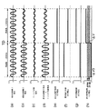
つぎに、本実施形態において、表示制御回路61CのマイクロコンピュータMCによって、発振回路41Cの発振周波数が1.00MHzから1.02MHzに変化される場合の動作について図10及び図11を用いて説明する。図10は、駆動状態の波形図であり、図11は非駆動状態の波形図である。図10及び図11において、(a)は超音波振動子1に付与される電圧の波形であり、(b)は超音波振動子1に流れる電流の波形であり、(c)は、フィルタ回路421Cから接地側に流れる電流の波形であり、(d)は超音波振動子1に流れる電流とフィルタ回路421Cから接地側に流れる電流との和(すなわち、フィルタ回路421Cに流れる電流)の波形であり、(e)は増幅回路42Cの直流定電圧電源の出力電流の波形であり、(f)は電流検出回路54Cの出力電圧の波形であり、(g)は信号増幅回路55Cの出力電圧の波形であり、(h)は表示制御回路61Cの入力電圧である。図10及び図11の横軸は時間であって、横軸方向の略中央部の時間TD(TE)の左側は、発振回路41Cの発振周波数が1.00MHzの状態であり、時間TD(TE)の右側は、発振回路41Cの発振周波数が1.02MHzの状態である。
【0037】
駆動状態においては、図10に示すように、発振回路41Cの発振周波数が1.00MHzから1.02MHzに変化された場合に、振動部10のインピーダンスが20Ωから200Ωに増大するため、超音波振動子1に流れる電流は減少し、フィルタ回路421Cの減衰量は変化しない(0dB)ため、フィルタ回路421Cから接地側に流れる電流は変化しない。そこで、超音波振動子1に流れる電流とフィルタ回路421Cから接地側に流れる電流との和は減少し、増幅回路42Cの直流定電圧電源の出力電流は減少し、信号増幅回路55Cの出力電圧及び表示制御回路61Cの入力電圧が増大する。そして、表示制御回路61CのマイクロコンピュータMCによって、表示制御回路61Cの入力電圧の変化量ΔVが算出されて、この変化量ΔVが所定の基準値ΔV0以上であるため、表示制御回路61Cによって表示信号は出力されず(出力が5Vとなり)、表示回路62Cのスイッチ用トランジスタがオフしたままとなるのでLEDには電源からの電流が流れず、LEDは消灯状態となる。
【0038】
非駆動状態においては、図11に示すように、発振回路41Cの発振周波数が1.00MHzから1.02MHzに変化された場合に、超音波振動子1に流れる電流は0であり、フィルタ回路421Cの減衰量は変化しない(0dB)ため、フィルタ回路421Cに流れる電流は変化しない。そこで、超音波振動子1に流れる電流とフィルタ回路421Cに流れる電流との和の電流は変化せず、増幅回路42Cの直流定電圧電源の出力電流も変化せず、信号増幅回路55Cの出力電圧及び表示制御回路61Cの入力電圧も変化しない。そして、表示制御回路61CのマイクロコンピュータMCによって、表示制御回路61Cの入力電圧の変化量ΔVが0と算出されて、この変化量ΔV(=0)が所定の基準値ΔV0未満であるため、表示制御回路61Cによって表示信号は出力され(出力が0Vとなり)、表示回路62Cのスイッチ用トランジスタがオンして電源からLEDに電流が流れるので、LEDが点灯状態となる。
【0039】
このようにして、マイクロコンピュータMCによって、超音波振動子1を駆動する周波数である駆動周波数が変更され、検出部5Cによって、マイクロコンピュータMCによる駆動周波数の変更に伴う駆動電流の変化を検出することにより超音波振動子1へ電力が供給されているか否かが検出されるため、駆動部4Cがノイズ対策のためのLC回路等からなるフィルタ回路421Cを備える場合にも超音波振動子1へ電力が供給されているか否かを検出することができる。
【0040】
なお、駆動周波数を変更すると超音波美容器から肌に付与される超音波の出力が変化するため、超音波美容器を使用中に駆動周波数を変更することは好ましくない。そこで、マイクロコンピュータMCによって駆動周波数を変更するタイミングは、電源投入から利用者がホーン2を肌に当てる迄の間等の電源が「ON」の状態で且つ超音波美容器を使用中ではない(肌に超音波刺激を付与していない)時に行うものとする。例えば、電源投入から所定の短い時間中に行えばよい。また、駆動周波数は、自動で1.00MHzから1.02MHzに変更される。
【0041】
なお、本発明の超音波美容器は、上記実施形態のものに限定されるものではなく、以下に述べるように種々の変形態様を採用することができる。
(A)第1〜第4実施形態では、表示部がLEDの点滅によって検出部による検出結果を表示する場合について説明したが、他の方法によって検出部による検出結果を表示する形態でもよい。例えば、液晶モニタ等の表示部に文字メッセージを表示する形態でもよい。また、報知手段としては、検出結果を表示する態様の他、スピーカ等による警報等の検出結果を音声出力する態様でもよい。
(B)第1〜第4実施形態では、表示部が表示回路を備える場合について説明したが、電源の「ON/OFF」の表示等の他の目的で設けられた表示回路を共用する形態でもよい。この場合には、超音波美容器の構造が簡素化され、安価化が可能となる。
(C)第1〜第4実施形態では、検出部が駆動部から超音波振動子1に供給される電流を検出して、電圧に反転増幅して変換する場合について説明したが、反転及び増幅の少なくとも一方を行わない形態でもよい。
【0042】
【発明の効果】
請求項1に記載の発明によれば、駆動手段によって、超音波振動子に励振用の電力が供給され、超音波振動子によって、超音波が発生され、ホーンによって、放射面から超音波が肌に付与される。検出手段によって、駆動手段から超音波振動子へ電力が供給されているか否かが検出され、報知手段によって、検出手段による検出結果が報知されるため、超音波振動子に電力が供給されているか否かを容易に確認することが可能となる。
【0044】
また、請求項1に記載の発明によれば、検出手段によって、駆動手段から超音波振動子へ供給される駆動電流を検出することによって超音波振動子へ電力が供給されているか否かが検出されるため、超音波振動子に電力が供給されているか否かを簡単な回路構成で検出することが可能となる。
【0045】
また、請求項1に記載の発明によれば、周波数変更手段によって、超音波振動子を駆動する周波数である駆動周波数が変更され、検出手段によって、周波数変更手段による駆動周波数の変更に伴う駆動電流の変化を検出することにより超音波振動子へ電力が供給されているか否かが検出されるため、駆動手段がノイズ対策のためのLC回路等からなるフィルタ回路を備える場合にも超音波振動子へ電力が供給されているか否かを検出することができる。
【図面の簡単な説明】
【図1】 本発明の第1実施形態に係る超音波美容器の構成図である。
【図2】 第1実施形態の超音波美容器の動作を説明するための波形図である。
【図3】 本発明の第2実施形態に係る超音波美容器の回路図である。
【図4】 第2実施形態の超音波美容器の動作を説明するための波形図である。
【図5】 本発明の第3実施形態に係る超音波美容器の回路図である。
【図6】 第3実施形態の超音波美容器の動作を説明するための波形図である。
【図7】 本発明の第4実施形態に係る超音波美容器の回路図である。
【図8】 第4実施形態の超音波美容器の動作を説明するための波形図である。
【図9】 振動部のインピーダンス特性と、フィルタ回路の周波数特性の一例を示す図である。
【図10】 第4実施形態の超音波美容器の動作を説明するための波形図である(駆動状態)。
【図11】 第4実施形態の超音波美容器の動作を説明するための波形図である(非駆動状態)。
【図12】 従来の超音波美容器の構成図である。
【符号の説明】
1 超音波振動子
2 ホーン
3 プローブ
4、4A、4B、4C 駆動部(駆動手段)
41、41A、41B、41C 発振回路
42、42A、42B、42C 増幅回路
10 振動部
5 検出部(検出手段)
6 表示部(報知手段)
61、61A、61B、61C 表示制御回路
62、62A、62B、62C 表示回路
MC マイクロコンピュータ(周波数変更手段、報知手段の一部)[0001]
BACKGROUND OF THE INVENTION
The present invention relates to an ultrasonic cosmetic device in which an ultrasonic stimulation is applied to skin by bringing a vibrating part to which an ultrasonic transducer is attached into contact with skin such as a face.
[0002]
[Prior art]
In recent years, an ultrasonic vibration (ultrasonic stimulation) is imparted to the skin by bringing a vibrating portion formed by joining an ultrasonic transducer to a horn disposed at the tip of the probe into contact with the skin such as the face. Ultrasonic cosmetic instruments are known. FIG. 12 is a configuration diagram of a conventional ultrasonic cosmetic device. (A) is a whole block diagram, (b) is an enlarged block diagram of the vibration part mentioned later. The ultrasonic cosmetic device vibrates with a
[0003]
[Problems to be solved by the invention]
When using the ultrasonic cosmetic device as described above, if an excessive tension is applied between the
[0004]
However, the user of the ultrasonic cosmetic device determines whether or not ultrasonic vibration (ultrasonic stimulation) is applied to the skin from the
[0005]
The present invention has been made in view of the above problems, and an object of the present invention is to provide an ultrasonic cosmetic device capable of easily confirming whether electric power is supplied to an ultrasonic transducer.
[0006]
[Means for Solving the Problems]
An ultrasonic cosmetic device according to the present invention is an ultrasonic cosmetic device that applies ultrasonic stimulation to the skin, and an ultrasonic transducer that generates ultrasonic waves and a bonding surface joined to the ultrasonic transducer, and a radiation surface A probe having a vibrating part including a horn for applying ultrasonic waves to the skin, a driving unit that supplies power for excitation to the ultrasonic transducer, and power that is supplied from the driving unit to the ultrasonic transducer Detection means for detecting whether or not is, and notification means for notifying the detection result by the detection means,The driving unit includes a frequency changing unit that changes a driving frequency that is a frequency for driving the ultrasonic transducer, and the detecting unit detects a driving current supplied from the driving unit to the ultrasonic transducer. Thus, it is detected whether or not electric power is supplied to the ultrasonic transducer, and the ultrasonic transducer is detected by detecting a change in the drive current accompanying a change in the drive frequency by the frequency changing means. It is characterized by detecting whether or not electric power is supplied.
[0007]
According to the above configuration, the driving unit supplies excitation power to the ultrasonic transducer, the ultrasonic transducer generates ultrasonic waves, and the horn applies ultrasonic waves from the radiation surface to the skin. . Whether or not electric power is supplied from the driving means to the ultrasonic vibrator is detected by the detecting means, and whether or not electric power is supplied to the ultrasonic vibrator because the detection result is notified by the notifying means. It becomes possible to easily confirm whether or not.
[0009]
Also,According to the above configuration, the detection unit detects whether or not electric power is supplied to the ultrasonic transducer by detecting the drive current supplied from the drive unit to the ultrasonic transducer. It is possible to detect whether power is supplied to the vibrator with a simple circuit configuration.
[0010]
Also,According to the above configuration, the drive frequency that is the frequency for driving the ultrasonic transducer is changed by the frequency changing unit, and the change of the drive current accompanying the change of the drive frequency by the frequency changing unit is detected by the detecting unit. Therefore, it is detected whether or not power is supplied to the ultrasonic vibrator. Therefore, even when the driving means includes a filter circuit made up of an LC circuit or the like for noise countermeasures, power is supplied to the ultrasonic vibrator. It can be detected whether or not.
[0011]
DETAILED DESCRIPTION OF THE INVENTION
(1st Embodiment: An example of embodiment of the ultrasonic cosmetic device of Claim 1)
FIG. 1 is a configuration diagram of an ultrasonic cosmetic device according to the first embodiment of the present invention. The ultrasonic cosmetic device includes an
[0012]
The
[0013]
FIG. 2 is a waveform diagram for explaining the operation of the ultrasonic cosmetic device of the first embodiment. (A) is a waveform of a voltage applied to the
[0014]
In the driving state, a predetermined current flows through the
[0015]
Whether or not electric power is supplied from the
[0016]
(Second embodiment: an example of an embodiment of the ultrasonic cosmetic device according to claim 2)
FIG. 3 is a circuit diagram of an ultrasonic cosmetic device according to the second embodiment of the present invention. The ultrasonic cosmetic device includes an
[0017]
The
[0018]
The
[0019]
FIG. 4 is a waveform diagram for explaining the operation of the ultrasonic cosmetic device of the second embodiment. (A) is a waveform of a voltage applied to the
[0020]
In the driving state, a predetermined current flows through the
[0021]
In the non-driving state, no current flows through the
[0022]
The
[0023]
(Third embodiment: an example of an embodiment of an ultrasonic cosmetic device according to claim 3)
FIG. 5 is a circuit diagram of an ultrasonic cosmetic device according to the third embodiment of the present invention. The ultrasonic cosmetic device includes an
[0024]
The
[0025]
The
[0026]
FIG. 6 is a waveform diagram for explaining the operation of the ultrasonic cosmetic device of the third embodiment. (A) is the waveform of the voltage applied to the
[0027]
In the driving state, a predetermined current flows through the
[0028]
In the non-driving state, no current flows through the
[0029]
The
[0030]
(4th Embodiment: An example of embodiment of the ultrasonic cosmetic device of Claim 4)
FIG. 7 is a circuit diagram of an ultrasonic cosmetic device according to the fourth embodiment of the present invention. The ultrasonic cosmetic device includes an
[0031]
The
[0032]
The display unit 6C calculates a change amount ΔV of the input voltage of the
[0033]
FIG. 8 is a waveform diagram for explaining the operation of the ultrasonic cosmetic device of the fourth embodiment. (A) is the waveform of the voltage applied to the
[0034]
In the driving state, a predetermined current flows through the
[0035]
FIG. 9 is a diagram illustrating an example of impedance characteristics of the
[0036]
Next, in the present embodiment, an operation when the oscillation frequency of the oscillation circuit 41C is changed from 1.00 MHz to 1.02 MHz by the microcomputer MC of the
[0037]
In the driving state, as shown in FIG. 10, when the oscillation frequency of the oscillation circuit 41C is changed from 1.00 MHz to 1.02 MHz, the impedance of the
[0038]
In the non-driving state, as shown in FIG. 11, when the oscillation frequency of the oscillation circuit 41C is changed from 1.00 MHz to 1.02 MHz, the current flowing through the
[0039]
In this way, the drive frequency that is the frequency for driving the
[0040]
In addition, since the output of the ultrasonic wave provided to skin from an ultrasonic cosmetics device will change if a drive frequency is changed, it is not preferable to change a drive frequency while using an ultrasonic cosmetic device. Therefore, the timing for changing the driving frequency by the microcomputer MC is such that the power source is “ON” from when the power is turned on until the user touches the
[0041]
The ultrasonic cosmetic device of the present invention is not limited to the above-described embodiment, and various modifications can be adopted as described below.
(A) In the first to fourth embodiments, the case where the display unit displays the detection result by the detection unit by blinking the LED has been described. However, the detection result by the detection unit may be displayed by another method. For example, a form in which a text message is displayed on a display unit such as a liquid crystal monitor may be used. Moreover, as an alerting | reporting means, the aspect which outputs the detection results, such as an alarm by a speaker other than the aspect which displays a detection result, may be sufficient.
(B) In the first to fourth embodiments, the case where the display unit includes the display circuit has been described. However, the display circuit provided for other purposes such as the display of “ON / OFF” of the power supply may be shared. Good. In this case, the structure of the ultrasonic cosmetic device is simplified, and the cost can be reduced.
(C) In the first to fourth embodiments, a case has been described in which the detection unit detects the current supplied from the drive unit to the
[0042]
【The invention's effect】
According to the first aspect of the present invention, excitation power is supplied to the ultrasonic vibrator by the driving means, ultrasonic waves are generated by the ultrasonic vibrator, and ultrasonic waves are emitted from the radiation surface to the skin by the horn. To be granted. Whether or not electric power is supplied from the driving means to the ultrasonic vibrator is detected by the detecting means, and whether or not electric power is supplied to the ultrasonic vibrator because the detection result is notified by the notifying means. It becomes possible to easily confirm whether or not.
[0044]
Also,Claim1According to the invention described in (4), since it is detected whether or not electric power is supplied to the ultrasonic transducer by detecting the drive current supplied from the drive unit to the ultrasonic transducer, It becomes possible to detect whether electric power is supplied to the sonic transducer with a simple circuit configuration.
[0045]
Also,Claim1According to the invention described in (1), the drive frequency, which is the frequency for driving the ultrasonic transducer, is changed by the frequency changing means, and the change of the drive current accompanying the change of the drive frequency by the frequency changing means is detected by the detecting means. Therefore, whether or not electric power is supplied to the ultrasonic transducer is detected. Therefore, even when the driving means includes a filter circuit including an LC circuit for noise countermeasures, electric power is supplied to the ultrasonic transducer. It can be detected whether or not.
[Brief description of the drawings]
FIG. 1 is a configuration diagram of an ultrasonic cosmetic device according to a first embodiment of the present invention.
FIG. 2 is a waveform diagram for explaining the operation of the ultrasonic cosmetic device according to the first embodiment.
FIG. 3 is a circuit diagram of an ultrasonic cosmetic device according to a second embodiment of the present invention.
FIG. 4 is a waveform diagram for explaining the operation of the ultrasonic cosmetic device of the second embodiment.
FIG. 5 is a circuit diagram of an ultrasonic cosmetic device according to a third embodiment of the present invention.
FIG. 6 is a waveform diagram for explaining the operation of the ultrasonic cosmetic device of the third embodiment.
FIG. 7 is a circuit diagram of an ultrasonic cosmetic device according to a fourth embodiment of the present invention.
FIG. 8 is a waveform diagram for explaining the operation of the ultrasonic cosmetic device of the fourth embodiment.
FIG. 9 is a diagram illustrating an example of impedance characteristics of a vibration unit and frequency characteristics of a filter circuit.
FIG. 10 is a waveform diagram for explaining the operation of the ultrasonic cosmetic device of the fourth embodiment (driving state).
FIG. 11 is a waveform diagram for explaining the operation of the ultrasonic cosmetic device of the fourth embodiment (non-driven state).
FIG. 12 is a configuration diagram of a conventional ultrasonic cosmetic device.
[Explanation of symbols]
1 Ultrasonic transducer
2 Horn
3 Probe
4, 4A, 4B, 4C Drive unit (drive means)
41, 41A, 41B, 41C Oscillator circuit
42, 42A, 42B, 42C Amplifier circuit
10 Vibration part
5 Detection part (detection means)
6 Display (notification means)
61, 61A, 61B, 61C Display control circuit
62, 62A, 62B, 62C Display circuit
MC microcomputer (frequency change means, part of notification means)
Claims (1)
超音波を発生させる超音波振動子と、
接合面で前記超音波振動子に接合され、放射面から超音波を肌に付与するホーンとからなる振動部を備えたプローブと、
前記超音波振動子に励振用の電力を供給する駆動手段と、
前記駆動手段から前記超音波振動子へ電力が供給されているか否かを検出する検出手段と、
前記検出手段による検出結果を報知する報知手段とを備え、
前記駆動手段は、前記超音波振動子を駆動する周波数である駆動周波数を変更する周波数変更手段を備え、
前記検出手段は、前記駆動手段から前記超音波振動子へ供給される駆動電流を検出することによって前記超音波振動子へ電力が供給されているか否かを検出するものであり、前記周波数変更手段による駆動周波数の変更に伴う前記駆動電流の変化を検出することによって前記超音波振動子へ電力が供給されているか否かを検出することを特徴とする超音波美容器。 An ultrasonic cosmetic device that applies ultrasonic stimulation to the skin,
An ultrasonic transducer that generates ultrasonic waves;
A probe having a vibrating portion that is bonded to the ultrasonic transducer at a bonding surface and includes a horn that applies ultrasonic waves to the skin from a radiation surface;
Driving means for supplying power for excitation to the ultrasonic transducer;
Detecting means for detecting whether electric power is supplied from the driving means to the ultrasonic transducer;
Informing means for informing the detection result by the detecting means,
The driving means includes frequency changing means for changing a driving frequency that is a frequency for driving the ultrasonic transducer,
The detecting means detects whether or not electric power is supplied to the ultrasonic vibrator by detecting a driving current supplied from the driving means to the ultrasonic vibrator, and the frequency changing means An ultrasonic cosmetic device characterized by detecting whether or not electric power is supplied to the ultrasonic transducer by detecting a change in the drive current accompanying a change in the drive frequency due to.
Priority Applications (1)
| Application Number | Priority Date | Filing Date | Title |
|---|---|---|---|
| JP2001288950A JP3888112B2 (en) | 2001-09-21 | 2001-09-21 | Ultrasonic beauty device |
Applications Claiming Priority (1)
| Application Number | Priority Date | Filing Date | Title |
|---|---|---|---|
| JP2001288950A JP3888112B2 (en) | 2001-09-21 | 2001-09-21 | Ultrasonic beauty device |
Publications (2)
| Publication Number | Publication Date |
|---|---|
| JP2003093464A JP2003093464A (en) | 2003-04-02 |
| JP3888112B2 true JP3888112B2 (en) | 2007-02-28 |
Family
ID=19111517
Family Applications (1)
| Application Number | Title | Priority Date | Filing Date |
|---|---|---|---|
| JP2001288950A Expired - Fee Related JP3888112B2 (en) | 2001-09-21 | 2001-09-21 | Ultrasonic beauty device |
Country Status (1)
| Country | Link |
|---|---|
| JP (1) | JP3888112B2 (en) |
-
2001
- 2001-09-21 JP JP2001288950A patent/JP3888112B2/en not_active Expired - Fee Related
Also Published As
| Publication number | Publication date |
|---|---|
| JP2003093464A (en) | 2003-04-02 |
Similar Documents
| Publication | Publication Date | Title |
|---|---|---|
| US6176840B1 (en) | Ultrasonic cosmetic treatment device | |
| US8211132B2 (en) | Ultrasonic surgical apparatus | |
| JP3696034B2 (en) | Ultrasonic drive device and ultrasonic surgical device | |
| EP1103238A1 (en) | Torsional ultrasound handpiece | |
| JP2642515B2 (en) | Drive circuit with weighted converter and feedback mechanism | |
| JP4955549B2 (en) | Ultrasonic generator system | |
| KR20220079503A (en) | Portable Multi-Frequency Ultrasonic Beauty Equipment and Its Composition Method | |
| JPH0549647A (en) | Ultrasonic surgical operation device | |
| JP2014226318A (en) | Ultrasonic treatment apparatus | |
| TW423967B (en) | Ultrasonic beauty culture apparatus | |
| JPH08196638A (en) | Optimal EEG stimulator | |
| JP4230357B2 (en) | Ultrasonic generation system | |
| JP2003093464A (en) | Ultrasonic beauty device | |
| JP4191862B2 (en) | Cylindrical polymer piezoelectric membrane vibrator | |
| JP3486469B2 (en) | Drive device for piezoelectric vibrator | |
| JP6648049B2 (en) | Beauty appliance, beauty appliance probe switching method, and beauty appliance mode switching method | |
| JP3746631B2 (en) | Ultrasonic surgical device | |
| JP4151154B2 (en) | Ultrasonic sensor transmission circuit | |
| JP2006181291A (en) | Ultrasonic beauty device | |
| JP2001095875A (en) | Ultrasonic health and beauty equipment | |
| JP2001235538A (en) | Ultrasonic transmission / reception circuit and object detector for visually impaired person | |
| JP2002078716A (en) | Ultrasonic treatment equipment | |
| JP3826140B2 (en) | Ultrasonic drive | |
| JP4829565B2 (en) | Ultrasonic transducer drive circuit and ophthalmic ultrasonic therapy device using the circuit | |
| US7669478B2 (en) | Ultrasonic driving device with multi-frequency scanning |
Legal Events
| Date | Code | Title | Description |
|---|---|---|---|
| A621 | Written request for application examination |
Free format text: JAPANESE INTERMEDIATE CODE: A621 Effective date: 20040213 |
|
| A977 | Report on retrieval |
Free format text: JAPANESE INTERMEDIATE CODE: A971007 Effective date: 20060206 |
|
| A131 | Notification of reasons for refusal |
Free format text: JAPANESE INTERMEDIATE CODE: A131 Effective date: 20060214 |
|
| A521 | Written amendment |
Free format text: JAPANESE INTERMEDIATE CODE: A523 Effective date: 20060417 |
|
| TRDD | Decision of grant or rejection written | ||
| A01 | Written decision to grant a patent or to grant a registration (utility model) |
Free format text: JAPANESE INTERMEDIATE CODE: A01 Effective date: 20061107 |
|
| A61 | First payment of annual fees (during grant procedure) |
Free format text: JAPANESE INTERMEDIATE CODE: A61 Effective date: 20061120 |
|
| R150 | Certificate of patent or registration of utility model |
Free format text: JAPANESE INTERMEDIATE CODE: R150 |
|
| FPAY | Renewal fee payment (event date is renewal date of database) |
Free format text: PAYMENT UNTIL: 20091208 Year of fee payment: 3 |
|
| S533 | Written request for registration of change of name |
Free format text: JAPANESE INTERMEDIATE CODE: R313533 |
|
| FPAY | Renewal fee payment (event date is renewal date of database) |
Free format text: PAYMENT UNTIL: 20091208 Year of fee payment: 3 |
|
| R350 | Written notification of registration of transfer |
Free format text: JAPANESE INTERMEDIATE CODE: R350 |
|
| FPAY | Renewal fee payment (event date is renewal date of database) |
Free format text: PAYMENT UNTIL: 20091208 Year of fee payment: 3 |
|
| FPAY | Renewal fee payment (event date is renewal date of database) |
Free format text: PAYMENT UNTIL: 20101208 Year of fee payment: 4 |
|
| FPAY | Renewal fee payment (event date is renewal date of database) |
Free format text: PAYMENT UNTIL: 20111208 Year of fee payment: 5 |
|
| FPAY | Renewal fee payment (event date is renewal date of database) |
Free format text: PAYMENT UNTIL: 20121208 Year of fee payment: 6 |
|
| FPAY | Renewal fee payment (event date is renewal date of database) |
Free format text: PAYMENT UNTIL: 20121208 Year of fee payment: 6 |
|
| FPAY | Renewal fee payment (event date is renewal date of database) |
Free format text: PAYMENT UNTIL: 20131208 Year of fee payment: 7 |
|
| LAPS | Cancellation because of no payment of annual fees |