JP3952017B2 - 光学的に有効な多層膜を形成するための方法および装置 - Google Patents
光学的に有効な多層膜を形成するための方法および装置 Download PDFInfo
- Publication number
- JP3952017B2 JP3952017B2 JP2003512459A JP2003512459A JP3952017B2 JP 3952017 B2 JP3952017 B2 JP 3952017B2 JP 2003512459 A JP2003512459 A JP 2003512459A JP 2003512459 A JP2003512459 A JP 2003512459A JP 3952017 B2 JP3952017 B2 JP 3952017B2
- Authority
- JP
- Japan
- Prior art keywords
- film
- multilayer film
- substrate
- surface side
- protective film
- Prior art date
- Legal status (The legal status is an assumption and is not a legal conclusion. Google has not performed a legal analysis and makes no representation as to the accuracy of the status listed.)
- Expired - Lifetime
Links
- 238000000034 method Methods 0.000 title claims description 36
- 239000000758 substrate Substances 0.000 claims abstract description 71
- 238000004544 sputter deposition Methods 0.000 claims abstract description 22
- 230000003287 optical effect Effects 0.000 claims abstract description 21
- 229910052581 Si3N4 Inorganic materials 0.000 claims abstract description 8
- VYPSYNLAJGMNEJ-UHFFFAOYSA-N Silicium dioxide Chemical compound O=[Si]=O VYPSYNLAJGMNEJ-UHFFFAOYSA-N 0.000 claims abstract description 8
- HQVNEWCFYHHQES-UHFFFAOYSA-N silicon nitride Chemical compound N12[Si]34N5[Si]62N3[Si]51N64 HQVNEWCFYHHQES-UHFFFAOYSA-N 0.000 claims abstract description 6
- 229910052814 silicon oxide Inorganic materials 0.000 claims abstract description 4
- PMHQVHHXPFUNSP-UHFFFAOYSA-M copper(1+);methylsulfanylmethane;bromide Chemical compound Br[Cu].CSC PMHQVHHXPFUNSP-UHFFFAOYSA-M 0.000 claims abstract description 3
- TWNQGVIAIRXVLR-UHFFFAOYSA-N oxo(oxoalumanyloxy)alumane Chemical compound O=[Al]O[Al]=O TWNQGVIAIRXVLR-UHFFFAOYSA-N 0.000 claims abstract description 3
- 239000011241 protective layer Substances 0.000 claims abstract 4
- 230000001681 protective effect Effects 0.000 claims description 45
- 238000000151 deposition Methods 0.000 claims description 15
- 239000000463 material Substances 0.000 claims description 11
- 238000012545 processing Methods 0.000 claims description 8
- 239000007787 solid Substances 0.000 claims description 3
- 239000002356 single layer Substances 0.000 claims description 2
- 238000000889 atomisation Methods 0.000 claims 1
- 239000012528 membrane Substances 0.000 claims 1
- 239000010410 layer Substances 0.000 abstract description 13
- 239000010408 film Substances 0.000 description 116
- 230000015572 biosynthetic process Effects 0.000 description 16
- 230000008021 deposition Effects 0.000 description 12
- 239000007789 gas Substances 0.000 description 6
- 229910004298 SiO 2 Inorganic materials 0.000 description 5
- QVGXLLKOCUKJST-UHFFFAOYSA-N atomic oxygen Chemical compound [O] QVGXLLKOCUKJST-UHFFFAOYSA-N 0.000 description 5
- 239000001301 oxygen Substances 0.000 description 5
- 229910052760 oxygen Inorganic materials 0.000 description 5
- 230000008569 process Effects 0.000 description 5
- IJGRMHOSHXDMSA-UHFFFAOYSA-N Atomic nitrogen Chemical compound N#N IJGRMHOSHXDMSA-UHFFFAOYSA-N 0.000 description 4
- 238000000576 coating method Methods 0.000 description 4
- 230000002441 reversible effect Effects 0.000 description 4
- 239000013077 target material Substances 0.000 description 4
- 239000011248 coating agent Substances 0.000 description 3
- 230000008878 coupling Effects 0.000 description 3
- 238000010168 coupling process Methods 0.000 description 3
- 238000005859 coupling reaction Methods 0.000 description 3
- 230000006870 function Effects 0.000 description 3
- 239000011521 glass Substances 0.000 description 3
- 230000007246 mechanism Effects 0.000 description 3
- 230000004048 modification Effects 0.000 description 3
- 238000012986 modification Methods 0.000 description 3
- 238000002294 plasma sputter deposition Methods 0.000 description 3
- 239000010409 thin film Substances 0.000 description 3
- XKRFYHLGVUSROY-UHFFFAOYSA-N Argon Chemical compound [Ar] XKRFYHLGVUSROY-UHFFFAOYSA-N 0.000 description 2
- XUIMIQQOPSSXEZ-UHFFFAOYSA-N Silicon Chemical compound [Si] XUIMIQQOPSSXEZ-UHFFFAOYSA-N 0.000 description 2
- 239000002313 adhesive film Substances 0.000 description 2
- 229910052681 coesite Inorganic materials 0.000 description 2
- 229910052906 cristobalite Inorganic materials 0.000 description 2
- 238000010586 diagram Methods 0.000 description 2
- 238000001755 magnetron sputter deposition Methods 0.000 description 2
- 238000004519 manufacturing process Methods 0.000 description 2
- 229910052757 nitrogen Inorganic materials 0.000 description 2
- 239000012788 optical film Substances 0.000 description 2
- 229910052710 silicon Inorganic materials 0.000 description 2
- 239000010703 silicon Substances 0.000 description 2
- 239000000377 silicon dioxide Substances 0.000 description 2
- 235000012239 silicon dioxide Nutrition 0.000 description 2
- 229910052682 stishovite Inorganic materials 0.000 description 2
- 229910052905 tridymite Inorganic materials 0.000 description 2
- 229910010413 TiO 2 Inorganic materials 0.000 description 1
- GWEVSGVZZGPLCZ-UHFFFAOYSA-N Titan oxide Chemical compound O=[Ti]=O GWEVSGVZZGPLCZ-UHFFFAOYSA-N 0.000 description 1
- 239000003082 abrasive agent Substances 0.000 description 1
- 230000002411 adverse Effects 0.000 description 1
- CSDREXVUYHZDNP-UHFFFAOYSA-N alumanylidynesilicon Chemical compound [Al].[Si] CSDREXVUYHZDNP-UHFFFAOYSA-N 0.000 description 1
- 229910052782 aluminium Inorganic materials 0.000 description 1
- XAGFODPZIPBFFR-UHFFFAOYSA-N aluminium Chemical compound [Al] XAGFODPZIPBFFR-UHFFFAOYSA-N 0.000 description 1
- 229910052786 argon Inorganic materials 0.000 description 1
- 230000005540 biological transmission Effects 0.000 description 1
- 238000006243 chemical reaction Methods 0.000 description 1
- 238000011109 contamination Methods 0.000 description 1
- 238000000354 decomposition reaction Methods 0.000 description 1
- 230000003247 decreasing effect Effects 0.000 description 1
- 238000004925 denaturation Methods 0.000 description 1
- 230000036425 denaturation Effects 0.000 description 1
- 230000001419 dependent effect Effects 0.000 description 1
- 239000003989 dielectric material Substances 0.000 description 1
- 238000009826 distribution Methods 0.000 description 1
- 239000013013 elastic material Substances 0.000 description 1
- 238000005566 electron beam evaporation Methods 0.000 description 1
- 230000003028 elevating effect Effects 0.000 description 1
- 239000006261 foam material Substances 0.000 description 1
- 238000000227 grinding Methods 0.000 description 1
- 230000006872 improvement Effects 0.000 description 1
- 238000010884 ion-beam technique Methods 0.000 description 1
- 150000002500 ions Chemical class 0.000 description 1
- 239000000203 mixture Substances 0.000 description 1
- QJGQUHMNIGDVPM-UHFFFAOYSA-N nitrogen group Chemical group [N] QJGQUHMNIGDVPM-UHFFFAOYSA-N 0.000 description 1
- BPUBBGLMJRNUCC-UHFFFAOYSA-N oxygen(2-);tantalum(5+) Chemical compound [O-2].[O-2].[O-2].[O-2].[O-2].[Ta+5].[Ta+5] BPUBBGLMJRNUCC-UHFFFAOYSA-N 0.000 description 1
- RVTZCBVAJQQJTK-UHFFFAOYSA-N oxygen(2-);zirconium(4+) Chemical compound [O-2].[O-2].[Zr+4] RVTZCBVAJQQJTK-UHFFFAOYSA-N 0.000 description 1
- 230000036961 partial effect Effects 0.000 description 1
- 230000002093 peripheral effect Effects 0.000 description 1
- 229920003023 plastic Polymers 0.000 description 1
- 229920001084 poly(chloroprene) Polymers 0.000 description 1
- 238000012805 post-processing Methods 0.000 description 1
- 238000003672 processing method Methods 0.000 description 1
- 230000009993 protective function Effects 0.000 description 1
- 238000005546 reactive sputtering Methods 0.000 description 1
- 230000002829 reductive effect Effects 0.000 description 1
- 239000007921 spray Substances 0.000 description 1
- PBCFLUZVCVVTBY-UHFFFAOYSA-N tantalum pentoxide Inorganic materials O=[Ta](=O)O[Ta](=O)=O PBCFLUZVCVVTBY-UHFFFAOYSA-N 0.000 description 1
- OGIDPMRJRNCKJF-UHFFFAOYSA-N titanium oxide Inorganic materials [Ti]=O OGIDPMRJRNCKJF-UHFFFAOYSA-N 0.000 description 1
- 229910001928 zirconium oxide Inorganic materials 0.000 description 1
Images


Classifications
-
- G—PHYSICS
- G02—OPTICS
- G02B—OPTICAL ELEMENTS, SYSTEMS OR APPARATUS
- G02B1/00—Optical elements characterised by the material of which they are made; Optical coatings for optical elements
- G02B1/10—Optical coatings produced by application to, or surface treatment of, optical elements
-
- C—CHEMISTRY; METALLURGY
- C23—COATING METALLIC MATERIAL; COATING MATERIAL WITH METALLIC MATERIAL; CHEMICAL SURFACE TREATMENT; DIFFUSION TREATMENT OF METALLIC MATERIAL; COATING BY VACUUM EVAPORATION, BY SPUTTERING, BY ION IMPLANTATION OR BY CHEMICAL VAPOUR DEPOSITION, IN GENERAL; INHIBITING CORROSION OF METALLIC MATERIAL OR INCRUSTATION IN GENERAL
- C23C—COATING METALLIC MATERIAL; COATING MATERIAL WITH METALLIC MATERIAL; SURFACE TREATMENT OF METALLIC MATERIAL BY DIFFUSION INTO THE SURFACE, BY CHEMICAL CONVERSION OR SUBSTITUTION; COATING BY VACUUM EVAPORATION, BY SPUTTERING, BY ION IMPLANTATION OR BY CHEMICAL VAPOUR DEPOSITION, IN GENERAL
- C23C14/00—Coating by vacuum evaporation, by sputtering or by ion implantation of the coating forming material
- C23C14/22—Coating by vacuum evaporation, by sputtering or by ion implantation of the coating forming material characterised by the process of coating
- C23C14/56—Apparatus specially adapted for continuous coating; Arrangements for maintaining the vacuum, e.g. vacuum locks
- C23C14/564—Means for minimising impurities in the coating chamber such as dust, moisture, residual gases
-
- C—CHEMISTRY; METALLURGY
- C23—COATING METALLIC MATERIAL; COATING MATERIAL WITH METALLIC MATERIAL; CHEMICAL SURFACE TREATMENT; DIFFUSION TREATMENT OF METALLIC MATERIAL; COATING BY VACUUM EVAPORATION, BY SPUTTERING, BY ION IMPLANTATION OR BY CHEMICAL VAPOUR DEPOSITION, IN GENERAL; INHIBITING CORROSION OF METALLIC MATERIAL OR INCRUSTATION IN GENERAL
- C23C—COATING METALLIC MATERIAL; COATING MATERIAL WITH METALLIC MATERIAL; SURFACE TREATMENT OF METALLIC MATERIAL BY DIFFUSION INTO THE SURFACE, BY CHEMICAL CONVERSION OR SUBSTITUTION; COATING BY VACUUM EVAPORATION, BY SPUTTERING, BY ION IMPLANTATION OR BY CHEMICAL VAPOUR DEPOSITION, IN GENERAL
- C23C14/00—Coating by vacuum evaporation, by sputtering or by ion implantation of the coating forming material
- C23C14/22—Coating by vacuum evaporation, by sputtering or by ion implantation of the coating forming material characterised by the process of coating
- C23C14/50—Substrate holders
- C23C14/505—Substrate holders for rotation of the substrates
-
- G—PHYSICS
- G02—OPTICS
- G02B—OPTICAL ELEMENTS, SYSTEMS OR APPARATUS
- G02B1/00—Optical elements characterised by the material of which they are made; Optical coatings for optical elements
- G02B1/10—Optical coatings produced by application to, or surface treatment of, optical elements
- G02B1/11—Anti-reflection coatings
Landscapes
- Chemical & Material Sciences (AREA)
- Physics & Mathematics (AREA)
- Materials Engineering (AREA)
- Chemical Kinetics & Catalysis (AREA)
- Engineering & Computer Science (AREA)
- Mechanical Engineering (AREA)
- Metallurgy (AREA)
- Organic Chemistry (AREA)
- Optics & Photonics (AREA)
- General Physics & Mathematics (AREA)
- Physical Vapour Deposition (AREA)
- Surface Treatment Of Optical Elements (AREA)
- Surface Treatment Of Glass (AREA)
- Organic Low-Molecular-Weight Compounds And Preparation Thereof (AREA)
Description
Claims (12)
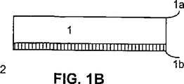
- 第1面側(1a)と第2面側(1b)とを有する基板(1)上に、プラズマ強化式の固体ターゲット原子化法(スパッタリング)によって、光学的に有効な多層膜(3)を形成する方法であって、
前記多層膜 (3) を形成するために使用される装置内で、スパッタリングにより前記基板(1)の前記第2面側(1b)に10〜40nmの厚さの保護膜(2)を付着し、次いで、前記基板の前記第1面側(1a)に前記多層膜(3)をスパッタリングすることを特徴とする方法。 - 前記保護膜(2)は、単層膜または前記第2面側に付着された追加の多層膜によって形成されることを特徴とする請求項1に記載の方法。
- 前記第1面側(1a)に前記多層膜(3)を形成した後、好ましくはその多層膜(3)を形成するために使用される装置内で、前記第2面側(1b)にさらなる多層膜(4)をスパッタリングすることを特徴する請求項1または2に記載の方法。
- 前記保護膜(2)は、その光学的特性が、前記さらなる多層膜(4)が満たすべき条件に適合するように選択または形成されることを特徴とする請求項3に記載の方法。
- 前記保護膜(2)は、ほぼ無酸素のプラズマを使用してスパッタリングされることを特徴とする請求項1から4のいずれか1項に記載の方法。
- 前記保護膜(2)は、前記多層膜 (3,4) 中の少なくともいくつかの膜を形成するために使用されるターゲットと同じターゲットを使用して形成されることを特徴とする請求項5に記載の方法。
- 前記保護膜(2)と前記多層膜 (3,4) 中の膜とを形成するために同じターゲットが使用され、プラズマを形成するための処理ガスは、形成する膜に応じて交換されることを特徴とする請求項6に記載の方法。
- 前記保護膜(2)は、酸化シリコン、窒化シリコン、酸化アルミニウム、または窒化アルミニウムのいずれかまたはこれらの組み合わせを含むことを特徴とする請求項1から7のいずれか1項に記載の方法。
- 前記保護膜(2)の材料および厚さは、前記多層膜 (3) を前記第1面側 (1a) に付着する間の処理パラメータに応じて、この多層膜 (3) が付着された後に、所定の厚さの前記保護膜 (2) が存在するように選択されることを特徴とする請求項1から8のいずれか1項に記載の方法。
- 前記保護膜(2)として機能する多層膜を前記第2面側 (1b) に付着した後、まず、所定の光学特性を得るために前記第1面側 (1a) を加工し、次に、前記第1面側 (1a) に前記多層膜 (3) を付着することを特徴とする請求項1から9のいずれか1項に記載の方法。
- 請求項1から10のいずれか1項に記載の方法を実行するための装置であって、
排気可能なスパッタリング室と基板 (1) のための装着要素 (6) を備えた基板ホルダ (5) とを有し、前記装着要素によって、前記基板 (1) は、前記基板の表面にほぼ平行な反転軸および前記基板の表面にほぼ垂直な回転軸の両方の軸回りに回転できることを特徴とする装置。 - 前記回転軸回りの回転動作および前記反転軸回りの回転動作のための共通の駆動装置 (10) を備えていることを特徴とする請求項11に記載の装置。
Applications Claiming Priority (2)
| Application Number | Priority Date | Filing Date | Title |
|---|---|---|---|
| EP01810698A EP1275751A1 (de) | 2001-07-13 | 2001-07-13 | Verfahren und Vorrichtung zur Herstellung eines optisch wirksamen Schichtsystems |
| PCT/EP2002/007141 WO2003006704A1 (de) | 2001-07-13 | 2002-06-28 | Verfahren und vorrichtung zur herstellung eines optisch wirksamen schichtsystems |
Publications (3)
| Publication Number | Publication Date |
|---|---|
| JP2004534154A JP2004534154A (ja) | 2004-11-11 |
| JP2004534154A5 JP2004534154A5 (ja) | 2005-06-02 |
| JP3952017B2 true JP3952017B2 (ja) | 2007-08-01 |
Family
ID=8184027
Family Applications (1)
| Application Number | Title | Priority Date | Filing Date |
|---|---|---|---|
| JP2003512459A Expired - Lifetime JP3952017B2 (ja) | 2001-07-13 | 2002-06-28 | 光学的に有効な多層膜を形成するための方法および装置 |
Country Status (8)
| Country | Link |
|---|---|
| US (1) | US6878243B2 (ja) |
| EP (2) | EP1275751A1 (ja) |
| JP (1) | JP3952017B2 (ja) |
| KR (1) | KR100570851B1 (ja) |
| CN (1) | CN1223700C (ja) |
| AT (1) | ATE406468T1 (ja) |
| DE (1) | DE50212709D1 (ja) |
| WO (1) | WO2003006704A1 (ja) |
Families Citing this family (12)
| Publication number | Priority date | Publication date | Assignee | Title |
|---|---|---|---|---|
| FR2834712B1 (fr) | 2002-01-14 | 2004-12-17 | Essilor Int | Procede de traitement d'un verre ophtalmique |
| FR2856056B1 (fr) | 2003-06-13 | 2009-07-03 | Essilor Int | Procede de traitement d'un verre apte au debordage. |
| FR2860306B1 (fr) | 2003-09-26 | 2006-09-01 | Essilor Int | Lentille ophtalmique recouverte d'un film electrostatique et procede de debordage d'une telle lentille |
| ATE494400T1 (de) | 2004-11-05 | 2011-01-15 | Satisloh Ag | Verfahren zum aufbringen optischer beschichtungen |
| US8454804B2 (en) * | 2005-10-28 | 2013-06-04 | Applied Materials Inc. | Protective offset sputtering |
| US8460519B2 (en) * | 2005-10-28 | 2013-06-11 | Applied Materials Inc. | Protective offset sputtering |
| US20070141358A1 (en) | 2005-12-19 | 2007-06-21 | Essilor International Compagnie Generale D'optique | Method for improving the edging of an optical article by providing a temporary layer of an organic material |
| WO2008120390A1 (ja) * | 2007-03-29 | 2008-10-09 | Ibiden Co., Ltd. | ハニカム構造体の製造方法およびハニカム構造体 |
| WO2012168709A2 (en) | 2011-06-07 | 2012-12-13 | Power Vision Limited | Improvements to the application of coating materials |
| JP2015023055A (ja) * | 2013-07-16 | 2015-02-02 | ソニー株式会社 | 電子装置、光ディスク装置、表示装置および撮像装置 |
| DE102016125273A1 (de) | 2016-12-14 | 2018-06-14 | Schneider Gmbh & Co. Kg | Anlage, Verfahren und Träger zur Beschichtung von Brillengläsern |
| CN113584448B (zh) * | 2021-07-27 | 2023-06-27 | 华天慧创科技(西安)有限公司 | 一种光学滤光片镀膜方法 |
Family Cites Families (4)
| Publication number | Priority date | Publication date | Assignee | Title |
|---|---|---|---|---|
| GB8921666D0 (en) * | 1989-09-26 | 1989-11-08 | Peatgrange Ivd Limited | Ion vapour deposition apparatus and method |
| DE4117257B4 (de) * | 1989-12-27 | 2006-03-30 | Unaxis Deutschland Holding Gmbh | Optisch wirkendes Schichtsystem mit hoher Antireflexwirkung für transparente Substrate |
| GB9317170D0 (en) * | 1993-08-18 | 1993-10-06 | Applied Vision Ltd | Improvements in physical vapour deposition apparatus |
| GB9405442D0 (en) * | 1994-03-19 | 1994-05-04 | Applied Vision Ltd | Apparatus for coating substrates |
-
2001
- 2001-07-13 EP EP01810698A patent/EP1275751A1/de not_active Withdrawn
-
2002
- 2002-06-28 KR KR1020037009378A patent/KR100570851B1/ko not_active Expired - Lifetime
- 2002-06-28 EP EP02751081A patent/EP1407059B1/de not_active Expired - Lifetime
- 2002-06-28 WO PCT/EP2002/007141 patent/WO2003006704A1/de not_active Ceased
- 2002-06-28 DE DE50212709T patent/DE50212709D1/de not_active Expired - Lifetime
- 2002-06-28 CN CNB028049136A patent/CN1223700C/zh not_active Expired - Lifetime
- 2002-06-28 AT AT02751081T patent/ATE406468T1/de not_active IP Right Cessation
- 2002-06-28 JP JP2003512459A patent/JP3952017B2/ja not_active Expired - Lifetime
-
2003
- 2003-11-04 US US10/700,996 patent/US6878243B2/en not_active Expired - Lifetime
Also Published As
| Publication number | Publication date |
|---|---|
| KR20040007436A (ko) | 2004-01-24 |
| JP2004534154A (ja) | 2004-11-11 |
| CN1491296A (zh) | 2004-04-21 |
| CN1223700C (zh) | 2005-10-19 |
| EP1407059B1 (de) | 2008-08-27 |
| DE50212709D1 (de) | 2008-10-09 |
| EP1275751A1 (de) | 2003-01-15 |
| EP1407059A1 (de) | 2004-04-14 |
| US20040089537A1 (en) | 2004-05-13 |
| ATE406468T1 (de) | 2008-09-15 |
| KR100570851B1 (ko) | 2006-04-12 |
| US6878243B2 (en) | 2005-04-12 |
| WO2003006704A1 (de) | 2003-01-23 |
Similar Documents
| Publication | Publication Date | Title |
|---|---|---|
| EP2054160B1 (en) | Method for producing smooth, dense optical films | |
| TWI564409B (zh) | 光學塗佈方法、設備與產品 | |
| JP3952017B2 (ja) | 光学的に有効な多層膜を形成するための方法および装置 | |
| KR102388528B1 (ko) | 나노-라미네이트 광학 코팅을 형성하기 위한 시스템 | |
| EP1274660B1 (en) | Method for applying an antireflection coating to inorganic optically transparent substrates | |
| EP0928977A1 (en) | Plastic optical component having a reflection prevention film and mechanism for making reflection prevention film thickness uniform | |
| EP2242867B1 (en) | A method of giving an article a coloured appearance and an article having a coloured appearance | |
| JP3808917B2 (ja) | 薄膜の製造方法及び薄膜 | |
| CN111999785B (zh) | 减反射膜、制备方法、减反射光学制品及应用 | |
| EP3751319A1 (en) | Optical thin film, optical member, and method for manufacturing optical thin film | |
| TW202415787A (zh) | 藉由磁控濺鍍以沉積量子化奈米層的方法 | |
| EP0573163A2 (en) | Enhanced durability optical stack such as a mirror and a process for forming the stack | |
| US20260126479A1 (en) | Vapor Cells Having Optical Windows with Multilayer Coatings | |
| Golling et al. | Dual Ion Beam Sputtering | |
| JPH1068802A (ja) | 反射防止膜及びその成膜法 | |
| JP2026003773A (ja) | 誘電体多層膜付き基板及びその製造方法、並びに光学多層膜付き基板の製造方法 | |
| CN119439340A (zh) | 一种滤光片及其制作方法与应用 | |
| JP2001262317A (ja) | 光学薄膜及びその製造方法 | |
| JP2000214303A (ja) | 反射防止膜等の光学薄膜及びその製造方法 | |
| HK1050354B (en) | Method for applying an antireflection coating to inorganic optically transparent substrates | |
| JPH05247643A (ja) | 合成樹脂製反射鏡及びその製造方法 |
Legal Events
| Date | Code | Title | Description |
|---|---|---|---|
| A977 | Report on retrieval |
Free format text: JAPANESE INTERMEDIATE CODE: A971007 Effective date: 20060724 |
|
| A131 | Notification of reasons for refusal |
Free format text: JAPANESE INTERMEDIATE CODE: A131 Effective date: 20060809 |
|
| A601 | Written request for extension of time |
Free format text: JAPANESE INTERMEDIATE CODE: A601 Effective date: 20061109 |
|
| A602 | Written permission of extension of time |
Free format text: JAPANESE INTERMEDIATE CODE: A602 Effective date: 20061120 |
|
| A521 | Request for written amendment filed |
Free format text: JAPANESE INTERMEDIATE CODE: A523 Effective date: 20070208 |
|
| TRDD | Decision of grant or rejection written | ||
| A01 | Written decision to grant a patent or to grant a registration (utility model) |
Free format text: JAPANESE INTERMEDIATE CODE: A01 Effective date: 20070322 |
|
| A61 | First payment of annual fees (during grant procedure) |
Free format text: JAPANESE INTERMEDIATE CODE: A61 Effective date: 20070416 |
|
| R150 | Certificate of patent or registration of utility model |
Free format text: JAPANESE INTERMEDIATE CODE: R150 Ref document number: 3952017 Country of ref document: JP Free format text: JAPANESE INTERMEDIATE CODE: R150 |
|
| FPAY | Renewal fee payment (event date is renewal date of database) |
Free format text: PAYMENT UNTIL: 20110511 Year of fee payment: 4 |
|
| R250 | Receipt of annual fees |
Free format text: JAPANESE INTERMEDIATE CODE: R250 |
|
| FPAY | Renewal fee payment (event date is renewal date of database) |
Free format text: PAYMENT UNTIL: 20120511 Year of fee payment: 5 |
|
| R250 | Receipt of annual fees |
Free format text: JAPANESE INTERMEDIATE CODE: R250 |
|
| FPAY | Renewal fee payment (event date is renewal date of database) |
Free format text: PAYMENT UNTIL: 20130511 Year of fee payment: 6 |
|
| R250 | Receipt of annual fees |
Free format text: JAPANESE INTERMEDIATE CODE: R250 |
|
| FPAY | Renewal fee payment (event date is renewal date of database) |
Free format text: PAYMENT UNTIL: 20130511 Year of fee payment: 6 |
|
| R250 | Receipt of annual fees |
Free format text: JAPANESE INTERMEDIATE CODE: R250 |
|
| R250 | Receipt of annual fees |
Free format text: JAPANESE INTERMEDIATE CODE: R250 |
|
| R250 | Receipt of annual fees |
Free format text: JAPANESE INTERMEDIATE CODE: R250 |
|
| R250 | Receipt of annual fees |
Free format text: JAPANESE INTERMEDIATE CODE: R250 |
|
| R250 | Receipt of annual fees |
Free format text: JAPANESE INTERMEDIATE CODE: R250 |
|
| R250 | Receipt of annual fees |
Free format text: JAPANESE INTERMEDIATE CODE: R250 |
|
| R250 | Receipt of annual fees |
Free format text: JAPANESE INTERMEDIATE CODE: R250 |
|
| R250 | Receipt of annual fees |
Free format text: JAPANESE INTERMEDIATE CODE: R250 |
|
| R250 | Receipt of annual fees |
Free format text: JAPANESE INTERMEDIATE CODE: R250 |
|
| R250 | Receipt of annual fees |
Free format text: JAPANESE INTERMEDIATE CODE: R250 |
|
| EXPY | Cancellation because of completion of term |